Surface and Thin Film Analysis II: Solving Real Problems in Materials, Nano and Bio
|
|
|
- Edwin Fox
- 5 years ago
- Views:
Transcription

1 Surface and Thin Film Analysis II: Solving Real Problems in Materials, Nano and Bio Mariano Anderle Promozione e internazionalizzazione del Sistema Trentino della Ricerca Dipartimento Innovazione, Ricerca e ICT Provincia Autonoma di Trento web: anderle@fbk.eu
2 Vacuum and Surfaces Dynamic and static SIMS Principle Instrumentation Applications Università di Torino, Corso di Laurea in Fisica 27 maggio 2009 Outline I and II XPS, Auger Principle Instrumentation Applications Surface Technique Integrated Use Some examples

3 Vacuum Coverage time t= 3x10⁻⁶ /p p pressure in mbar p ~ 10-6 mbar t ~ sec p ~ 10-9 mbar t ~ h t meas < t M.Anderle -SIMS- Università degli Studi di Torino, 26 maggio 2009
4 Vacuum Mean free path l l l 2.3* kt 1 2 d 2 p With p pressure in mbar and l mean free path in meter and T=300K: p ~ 10 3 mbar l ~ 2.3*10-7 m p ~ 10-3 mbar l ~ 2.3*10-1 m p ~ 10-6 mbar l ~ 2.3*10 2 m M.Anderle -SIMS- Università degli Studi di Torino, 26 maggio 2009 p


5 THE CLUSTER LABORATORY
6 Mass Spectrometry Base Process Particles Emission (Sputtering) Particles Emitted Ionization M.Anderle -SIMS- Università degli Studi di Torino, 26 maggio 2009
7 Analytical Modes of SIMS I S i J P Y i i Dynamic SIMS Static SIMS Material removal Elemental analysis Profiling Ultra surface analysis Elemental or molecular analysis Analysis complete before significant fraction of molecules destroyed M.Anderle -SIMS- Università degli Studi di Torino, 26 maggio 2009


8 Dynamic/Static I S i J P Y i i M.Anderle -SIMS-
9 Dynamic, Static and Imaging SIMS The Secondary Ion Mass Spectrometry technique (SIMS) is the most sensitive of all the commonly-employed surface analytical techniques - this is because of the inherent sensitivity associated with mass spectrometric-based techniques. secondary ions and neutrals (atoms and molecules) There are three different variants of the technique: uppermost layer primary ion Dynamic SIMS used for obtaining compositional information as a function of depth below the surface Static SIMS used for sub-monolayer elemental analysis Imaging SIMS used for spatially-resolved elemental analysis M.Anderle -SIMS-

 - high transmission - high lateral resolution - parallel detection Disadvantages: - analytical methodology not well defined - fixed incidence angle M.")
10 Platform Comparison Magnetic Sector (Cameca 6f) Quadrupole (PHI 1010) ToF-SIMS (TOF-SIMS IV) Advantages: - high mass resolution (20000) - high sensibility - good depth resolution - well defined analytical methodology Disadvantages: - related impact energy and angle - sputtering rate modification for grazing angle Advantages: - unrelated impact energy and angle - low impact energy - high depth resolution - well defined analytical methodology Disadvantages: - bad mass resolution (300) - bad sensibility Advantages: - high mass resolution (10000) - high transmission - high lateral resolution - parallel detection Disadvantages: - analytical methodology not well defined - fixed incidence angle M.Anderle -SIMS-
11 M.Anderle -SIMS- Dynamic SIMS: Depth Profile
12 Concentration (at/cm 3 ) 3keV Implant Normalized at 56 Si 2 ptp 1E21 1E20 As/Si 2E15 at/cm 3keV 1.0 kev 0.5 kev 0.3 kev Best detection 1 kev impact. 1E19 1E18 At 300 ev altered layer minimized 1E17 1E Depth (nm) M.Anderle -SIMS-
 1.")
13 Integrated SiF 4 Signal Per Cycle Growth Rate (A/Cycle) Intensity (A) CsW Counts Characterization of Temperature Effect on Film Growth SIMS Result 4.0x10⁻¹⁰ SiH 4 Exposure H 2 signal Purge WF 6 Exposure SiF 4 signal Purge 4x10 4 3x c 275 c 3.2x x10 4 1x c 175 c 2.4x Depth (nm) 1.6x *10-10 SIMS x * Scan Number Extent of reaction increases with surface temperature thermally activated process MS 1 W. Lei, L. Henn-Lecordier, M. Anderle, G. W. Rubloff, M. Barozzi and M. Bersani, Real-time observation and optimization of tungsten atomic layer deposition process cycle, J. Vac. Sci. Technol. B 24(2) (2006) p /T (K -1 ) 13
14 Mass Spectrum M.Anderle -SIMS-
15 Positive TOF-SIMS Spectrum of PET O O C O C O CH 2 CH Fragments allow the molecular structure of the polymer to be defined. m/z M.Anderle -SIMS- Università degli Studi di Torino, 26 maggio 2009
16 Positive TOF-SIMS Spectrum of PET M O CH CH M H H O C C 341 O (2M+H) O (3M+H) m/z The repeating peak patterns confirm the polymerization structure. M.Anderle -SIMS- Università degli Studi di Torino, 26 maggio 2009
17 Delay [ps] Microelectronics: Low K Materials Low-k for faster interconnects and improved device performances Al + SiO 2 interconnects slower circuit speed time to propagate signal along interconnect between devices is an RC delay metal Al ( 3.0 mw cm) dielectric SiO 2 (K=4.0) Cu ( 1.7 mw cm) low-k (K=2.0) device alone Generation (MFS, µm) Cu + low K interconnects faster low-k is achieved by decreasing bond polarizability (using organosilicate, polymers, ) lowering the density (foamed and porous materials)
18 Microelectronics: Low K Materials low-k matrix resin (PMSSQ) porogen (PMMA co-dmaema) solvents PROCESS FLOW SCHEMATIC spin-casting of porous low-k film spin casting annealing initial cure final cure template formation porogen volatilization MATERIALS characteristics ELECTRICAL PROPERTIES depend on both: STRUCTURE pores quality/quantity transformations & kinetics
19 i nt ensi t y Microelectronics: Low K Materials i nt ensi t y TOF SIMS i nt ensi t y x C x x600 x C x 1 h x600 high mass ions progressively disappear upon annealing Compression Fact or : mass Compression Fact or : mass MSSQ, transformation upon curing SSIMS, negative SI x C x 2 h 0. 6 self-consistent identification of the key species 0. 4 x600 key peaks intensity depends on the annealing T Compression Fact or : mass
20 intensity Microelectronics: Low K Materials C x 3' 125 C x 1h 225 C x 1h 275 C x 1h 325 C x 1h 450 C x 2h pure, 50 C x 3' POROGEN,transformations upon curing Pseudo-DSIMS, negative SI SI species selectively related to PMMA and DMAEMA DMAEMA cleavage and C (90%) remaining transforms by > 325 C PMMA no apparent trasformation until > 325 C 1 D OD CN C2N CNO C5 C6 C8 C9 PMMA fragments DMAEMA ligand porogen backbone NO backbone alteration until > 325 C NO porogen residuals by 450 C CD 2 CD 3 C x CH 2 CH 3 C y C O C O O CD 3 CH 2 N O CH 2 DEDUCTIONS: a different behavior for the ligand / backbone, PMMA / DMAEMA is observed the residual amount of porogen vs curing T can be evaluated CH 3 CH 3 TOF SIMS
21 relative intensity Microelectronics: Low K Materials low-k transformations: the actual chemical/compositional state of MSSQ is depicted by SSIMS polymerization / crosslinking is pointed out by the vanishing of the key species (PMSSQs oligomers) porogen transformations: mechanisms and kinetics are illustrated by the markers related to the PMMA/DMAEMA ligand / backbone appearance of porogen precipitates 10 0 fading of precipitates Several features of MATERIALS TRASFORMATIONS and KINETICS in the FORMATION of porous low-k can be evaluated by means of ToF-SIMS PMSSQ degree of curing Si 7O C 107 H 21 (pos. SI) Si 6O C 105 H 15 (neg. SI) PMMA DMAEMA different behavior for PMMA and DMAEMA MATRIX and POROGEN transformations are COMPETING upon curing. The transformation kinetics can influence the final low-k electrical properties and requires to be evaluated annealing T [ C]

22 M.Anderle -SIMS- Imaging SIMS


23 Images Spatial resolution Spatial resolution

24 M.Anderle -SIMS- Ion sources


25 Microelectronics: Low K Materials TOF SIMS POROGEN,transformations upon curing imaging ToF-SIMS, negative SI POROGEN AGGLOMERATES as spun / curing < 225 C agglomerates density depends on curing T agglomerates composition (PMMA/DMAEMA ligand/backbone) depends on curing T lateral inhomogeneities 225 C < curing < 450 C Field of view: 10.0 x 10.0 mm 2 2 mm DEDUCTION: porogen transformation includes precipitation and segregation phenomena

26 M.Anderle -SIMS- Images

27 Images AgBr microcrystals Br red I yellow Cl white Dopant segregation at grain boundaries of alumina M.Anderle -SIMS-

28 Images Localization of In and Al in kidney cells M.Anderle -SIMS-

29 M.Anderle -SIMS- Images

30 M.Anderle -SIMS- Images
31 Main advantages and drawbacks ADVANTAGES Sensitivity 1ppm-1ppb All elements are detectable Isotopic detection Good depth resolution Lateral resolution Quantification Insulators are analyzable DRAWBACKS Ion yield up to 6 orders of magnitude Strong matrix effects Depth resolution depends on sample morphology Specific standards are required Destructive technique
32 Ejected Electrons Elastic reflected electrons (BE) Secondary electrons (SE) Differentiated Auger spectrum Auger electrons BE which lost characteristic energy: core level ionization plasmon excitation Kinetic Energy (ev)

33 Escape depth l as a function of electron energy
34 XPS-ESCA X-ray Photoelectron Spectroscopy Electron Spectroscopy for Chemical Analysis
35 XPS electrons (E 0, k 0, s) electrons (E, k, s) atoms (E 0, k 0, Z) ions (E 0, k 0, Z) sample atoms (E, k, Z) ions (E, k, Z) e.m.radiation (hn 0, k 0, polarization) e.m. radiation (hn, k, polarization)
36 Principle Base principle of the technique is the photoelectric effect

37 Principle
38 Principle Electrons ejected from the solid surface keep memory of the chemical element are coming from! Beeing able to discriminate photoelectrons with different energy means to measure the chemical composition of the solid surface!
39 Apparatus Electron Energy Analyser e - Detector Source e - hn Sample Chamber Load Lock Pumping System
40 Vacuum To avoid the electron collisions in the path from surface to analyzer => P<10-3 Pa To avoid surface contamination during the measurements => P<10-6 Pa => The electron spectroscopy techniques utilize Ultra High Vacuum (UHV) conditions
41 Source Analyser E k hn F Vacuum Level Fermi Level E k =hn - E b - F Core level hn=> X Photons => XPS => Core Level UV Photons => UPS => Valence Band
42 Source E k = f ( E B ) E B is specifically related to the chemical element where the electron is coming from! measuring E k of the ejected electrons we can study the elemental chemistry of the sample surface. the photoelectronic peak width E k is directly correlated to the width of source peak hn, beeing the core level peak negligible and the work function F constant.
43 Source Main features: hn ~ 1 kev FWHM < 1 ev Intense beam Compatible with UHV


44 Source
 limits the energy resolution.")

45 Source The presence of a background radiation (Bremsstrahlung) limits the energy resolution. An aluminum foil between the source and the sample helps to reduce this Bremsstrahlung effects!

46 Source Monocromatic source

47 Source To focus monocromatic X ray beam on the sample, quartz crystal, X ray source and sample have to stay on the same circle (Rowland circle).
48 Other sources UV Sources Gas discharge He I (21.2 ev), He II (40.8 ev) Syncrotron radiation Monocromatic light with high intensity and variable energy

49 Analyzer CHA - Concentric Hemisphere Analyzer V 2 - V 1 = U k = U e (R 2 /R 1 - R 1 /R 2 )
 titanium alloy plasma treatment for -NH 2 introduction 26/05/2009")
50 OPTIMISATION OF SOFT TISSUE ADHESION TO DENTAL IMPLANTS Implanted titanium screw polished and smooth transmucosal collar abutment of titanium alloy integrin receptor gingival cell membrane polished cervical margin Peptide adhesion rough endosseous part (pure titanium) titanium alloy plasma treatment for -NH 2 introduction 26/05/


51


52

53
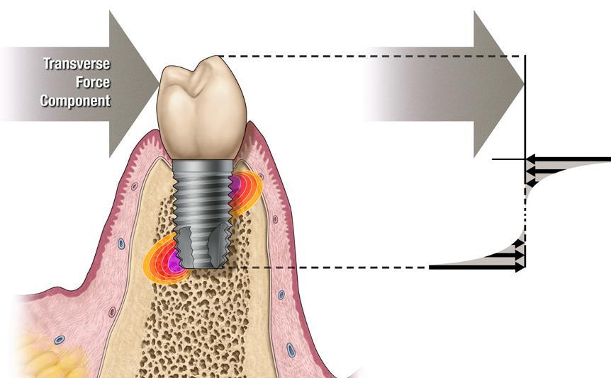

54 Resistance to transverse force component

55 Shorter to avoide neurological problems
56 Deporter, D.A., Todescan, R. et al. Length (mm) # Used # Failure % Failure , ,5 Overall 5 year failure rate = 4,6%
 surface; - Cell adhesive, RGD-containing peptides")
57 A Biological Functionalization to Stimulate the Soft Tissue Adhesion - Titanium alloy surface coating using a plasma assisted chemical vapor deposition process (PACVD) to reduce ion release from titanium and provide an amine-containing layer with adequate stability; - PEG molecules immobilization creating a protein-resistant (nonfouling) surface; - Cell adhesive, RGD-containing peptides immobilization stimulating the formation of the biological seal between the soft tissue and the implant.
58 Counts Spectrum O XPS survey spectrum Ti N C Binding energy (ev) UHV Plasma treatmentson Ti Al V alloy surface for primary amine (NH 2 ) group links
59 Counts Spectrum 9000 NH other N species 6000 NH Binding energy (ev) UHV Plasma treatmentson Ti Al V alloy surface for primary amine (NH 2 ) group links

60 ECM proteins and integrin receptors Fibronectin GLY-ARG-GLY-ASP- -SER-TYR-CYS b RGD Adhesion Peptide
 Step 2: thiol chemistry (Vinylsulfone) Fluorescent derivative PEG: 5.")
61 Titanium alloy functionalization: Overview Step 1: amide bond through the N-hydroxysuccinimide ester (NHS) Step 2: thiol chemistry (Vinylsulfone) Fluorescent derivative PEG: molecules/cm 2

62 Titanium alloy functionalization: XPS analysis?
 adhesion titanium alloy")

 and with a scanning")

63 Titanium alloy functionalization: Human gingival cells (HGF-1) adhesion titanium alloy a RGD modified titanium alloy b b1 cells density on different substrates a1 TiC+pep Ti Ti+pep TiC Cell images obtained with a laser scan microscope (a and b) and with a scanning electron microscope (a1 and b1) cell/cm 2 Incubation 24 h in serum free medium plus cycloheximide (25 ug/ml)
")


64 Carbon spectrum Oxygen spectrum Electron spectroscopy (ESCA) analysis of chitosan films chitosan is obtained from chitin by deactylation. Chitin Chitosan Nitrogen spectrum OH OH CH 2 CH 2 CH O CH O O - CH CH + CH CH O + O OH - C O CH CH CH CH CH 3 OH O C NH OH NH 2 n CH 3 n
65 Spectrum Different energy lines (different values of E B ) describing different core levels characteristic of the specific material (Pd). Auger line too!
66 CHEMICAL SHIFT

67 Quantification Relative sensitivity factors
68 Depth Profiling

69 Depth Profiling


70 Spectromicroscopy Increasing the lateral resolution of the technique focusing the X rays on a small surface area detecting the electrons from a small surface area

71 Spatial mode
72 Microelectronics: Oxynitrides 0.25 mm 0.10 mm Oxynitrides advantages with respect to conventional SiO 2 : good masking characteristic against impurity and dopant diffusion better resistance to dielectric breakdown better resistance to radiation damage and carrier injection suitable dielectric constant good technological compatibility with new generation materials


73 Microelectronics: Oxynitrides Precursor: Thermal treatment: Reoxidation: N 2 O NO Dry Wet Furnace RTA Sample # Oxidation Precursor Temperature Time 1 Dry N 2 O T2 t 2 Dry N 2 O T3 t 3 Dry N 2 O T3 2t 4 Wet N 2 O T2 t 5 Wet N 2 O T3 t 6 Dry NO T1 1.5t 7 Dry NO T1 3t 8 Dry NO T1 6t 9 Dry NO T2 3t 10 Dry NO T2 6t Thickness 10 nm SiO 2 SiO x N y Nitrided region Si
74 Microelectronics: Oxynitrides Dynamic SIMS Vacuum: <10-7 Torr Sputtering Rate: Å/s Primary Ions Energy: kev Primary Beam Current Density: na/cm 2 ma/cm 2 Useful to obtain: Depth Profile Mass Spectra Bulk Analysis Ion Images
75 Microelectronics: Oxynitrides Biomaterials surface chemical composition chemical bonds DETECTOR E K h n E B = 90 d = 5-6nm = 165 d = 2-3nm X RADIATION PHOTOELECTRONS XPS (X-ray Photoelectron Spectroscopy)
76 Counts (a.u.) Microelectronics: Oxynitrides Dynamic SIMS CsN + CsO + CsSi + Cs 2 N + Cs 2 O + Cs 2 Si Depth (A)
77 Concentration (at/cm 3 ) Microelectronics: Oxynitrides Dynamic SIMS Counts SiO 2 /Si interface Si sample 1 sample 2 sample 3 sample 4 sample N 2 O Distance to Interface (nm)
78 Concentration (at/cm 3 ) Microelectronics: Oxynitrides Dynamic SIMS Counts SiO 2 /Si interface Si sample 6 sample 7 sample 8 sample 9 sample NO Distance to Interface (nm)
79 Atomic Concentration (%) Microelectronics: Oxynitrides 4 SiO 2 /Si interface Nitrogen Profiles sample 1 sample 2 sample 3 sample 4 sample 5 sample 8 sample 9 sample Residual thickness (nm) XPS (X-ray Photoelectron Spectroscopy)
80 Microelectronics: Oxynitrides Sample # N integral (at/cm 2 ) SIMS peak concentration (at/cm 3 ) Peak position (nm) XPS peak concentration (%) x x x x x x x x x x x x x x x x x x x x
81 Photoemission Intensity (a.u.) E N1s (ev) Microelectronics: Oxynitrides N 1s interface sample 3 sample sample 1 sample 2 sample 3 sample 4 sample 5 sample 8 sample 9 sample 10 SiO 2 /Si interface E N1s in Si 3 N 4 peak bulk Binding Energy (ev) Residual Thickness (nm) XPS (X-ray Photoelectron Spectroscopy)
82 Surface and Interface Analysis TECHNIQUE XPS AES UPS SIMS TOF-SIMS SNMS XRD Source X-Ray (Mg, Al) Electrons Photons UV (HeI, HeII) Ions Ions Ions X-Ray (Cu) Particle Lateral Resolution Photo- Electrons Auger Electrons Photo- Electrons Secondary Ions Secondary Ions Neutrals postionized X-Ray 10 µm 0-2 µm No 0.5 µm 0-1 µm No No Sensitivity 0.1 % at. 0.1% at. Sampling Depth Main Features 2 20 atomiclayers Information on chemical bond 2 20 atomiclayers High spatial resolution Parameter without meaning 2 3 atomiclayers High sensitivity to valence band % at. 2 3 atomiclayers High sensitivity to elements % at. 2 3 atomiclayers Information on surface chemistry % at. 2 3 atomiclayers Elemental Sensitivity & Easy quantification 0.5 % at. 50 µm Structural Information SCIENTA 200 Physical Electronics PHI 590 PHI 4200 Physical Electronics PHI 545 CAMECA IMS 4f CAMECA SC Ultra CAMECA ION TOF IV Leybold Heraeus INA 3 Instrument at ITCirst Italstructures
83 A E S AES Auger Electron Spectroscopy
84 AES electrons (E 0, k 0, s) electrons (E, k, s) atoms (E 0, k 0, Z) ions (E 0, k 0, Z) sample atoms (E, k, Z) ions (E, k, Z) e.m.radiation (hn 0, k 0, polarization) e.m. radiation (hn, k, polarization)

85 Principle A E S Possible de-excitation processes due to electron bombardment
86 Auger and fluorescence efficency for a K vacancy as a function of atomic number, Z
87 Auger (continuos) and fluorescence (dashed) efficiency for K, L, M vacancies as a function of atomic number, Z

88 AES A E S

89 AES A E S
 Peak intensity ==> How much")
90 AES Analytical information from: Peak energy ==> What (qualitative) Peak shape and energy ==>How (chemistry) Peak intensity ==> How much (quantitative)


91 AES Spectrum A E S


92 Transition elements 3d
93 Transition elements 3d Characteristic features LMM triplet: L 3 M 2,3 M 2,3 L 3 M 2,3 V L 3 VV Peak M 2,3 VV at lower energy M 2,3 VV L 3 M 2,3 M 2,3 L 3 M 2,3 V L3 VV
94 dn(e)/de N(E) Energy ==> information about the chemical elements Ni Ni Ni O Ni S Cl C Kinetic Energy (ev) Ni S Cl C Ni Ni O Ni Kinetic Energy (ev)
95 dn(e)/de N(E)/E dn(e)/de N(E)/E Intensity [arb. units] Auger line energy and shape ==> information about element chemistry Example: Si LVV Silicon Oxide Silicon Oxide diamante carbonio amorfo grafite policristallina Kinetic Energy [ev] Example: C KVV Kinetic Energy [ev] Elemental Silicon Kinetic Energy [ev] Elemental Silicon Kinetic Energy [ev] Kinetic Energy [ev]
96 Analyzer A E S CMA Cilindric Mirror Analyzer

97 AES apparatus A E S
98 AUGER depth profiling A E S
99 concentrazione atomica relativa Ni1 Cr2 O tempo di sputtering [min] Cr 50nm Ni 65nm Cr

100
Processing and Characterization of PMSSQ Based Materials for Nanoporous Low-K Dielectrics
 Processing and Characterization of PMSSQ Based Materials for Nanoporous Low-K Dielectrics P. Lazzeri 1, L. Vanzetti 1, M. Bersani 1, M. Anderle 1, J.J. Park 2, Z. Lin 2,, R.M. Briber 2, G.W. Rubloff 2,
X-Ray Photoelectron Spectroscopy (XPS) Prof. Paul K. Chu
 Prof. Paul K. Chu") X-Ray Photoelectron Spectroscopy (XPS) Prof. Paul K. Chu X-ray Photoelectron Spectroscopy Introduction Qualitative analysis Quantitative analysis Charging compensation Small area analysis and XPS imaging
X-Ray Photoelectron Spectroscopy (XPS) Prof. Paul K. Chu X-ray Photoelectron Spectroscopy Introduction Qualitative analysis Quantitative analysis Charging compensation Small area analysis and XPS imaging
Methods of surface analysis
 Methods of surface analysis Nanomaterials characterisation I RNDr. Věra Vodičková, PhD. Surface of solid matter: last monoatomic layer + absorbed monolayer physical properties are effected (crystal lattice
Surface and Interface Characterization of Polymer Films
 Surface and Interface Characterization of Polymer Films Jeff Shallenberger, Evans Analytical Group 104 Windsor Center Dr., East Windsor NJ Copyright 2013 Evans Analytical Group Outline Introduction to
IV. Surface analysis for chemical state, chemical composition
 IV. Surface analysis for chemical state, chemical composition Probe beam Detect XPS Photon (X-ray) Photoelectron(core level electron) UPS Photon (UV) Photoelectron(valence level electron) AES electron
Introduction to X-ray Photoelectron Spectroscopy (XPS) XPS which makes use of the photoelectric effect, was developed in the mid-1960
 XPS which makes use of the photoelectric effect, was developed in the mid-1960") Introduction to X-ray Photoelectron Spectroscopy (XPS) X-ray Photoelectron Spectroscopy (XPS), also known as Electron Spectroscopy for Chemical Analysis (ESCA) is a widely used technique to investigate
Introduction to X-ray Photoelectron Spectroscopy (XPS) X-ray Photoelectron Spectroscopy (XPS), also known as Electron Spectroscopy for Chemical Analysis (ESCA) is a widely used technique to investigate
Material Characterization and the Formation of Nanoporous PMSSQ Low-K Dielectrics
 Material Characterization and the Formation of Nanoporous PMSSQ Low-K Dielectrics P. Lazzeri, L. Vanzetti, E. Iacob, M. Bersani, M. Anderle, J.J. Park, Z. Lin, R.M. Briber, G.W. Rubloff, R.D. Miller ITC-irst,
ToF-SIMS or XPS? Xinqi Chen Keck-II
 ToF-SIMS or XPS? Xinqi Chen Keck-II 1 Time of Flight Secondary Ion Mass Spectrometry (ToF-SIMS) Not ToF MS (laser, solution) X-ray Photoelectron Spectroscopy (XPS) 2 3 Modes of SIMS 4 Secondary Ion Sputtering
Secondaryionmassspectrometry
 Secondaryionmassspectrometry (SIMS) 1 Incident Ion Techniques for Surface Composition Analysis Mass spectrometric technique 1. Ionization -Electron ionization (EI) -Chemical ionization (CI) -Field ionization
Application of Surface Analysis for Root Cause Failure Analysis
 Application of Surface Analysis for Root Cause Failure Analysis David A. Cole Evans Analytical Group East Windsor, NJ Specialists in Materials Characterization Outline Introduction X-Ray Photoelectron
X-Ray Photoelectron Spectroscopy (XPS) Auger Electron Spectroscopy (AES)
 Auger Electron Spectroscopy (AES)") X-Ray Photoelectron Spectroscopy (XPS) Auger Electron Spectroscopy (AES) XPS X-ray photoelectron spectroscopy (XPS) is one of the most used techniques to chemically characterize the surface. Also known
X-Ray Photoelectron Spectroscopy (XPS) Auger Electron Spectroscopy (AES) XPS X-ray photoelectron spectroscopy (XPS) is one of the most used techniques to chemically characterize the surface. Also known
5) Surface photoelectron spectroscopy. For MChem, Spring, Dr. Qiao Chen (room 3R506) University of Sussex.
 Surface photoelectron spectroscopy. For MChem, Spring, Dr. Qiao Chen (room 3R506) University of Sussex.") For MChem, Spring, 2009 5) Surface photoelectron spectroscopy Dr. Qiao Chen (room 3R506) http://www.sussex.ac.uk/users/qc25/ University of Sussex Today s topics 1. Element analysis with XPS Binding energy,
For MChem, Spring, 2009 5) Surface photoelectron spectroscopy Dr. Qiao Chen (room 3R506) http://www.sussex.ac.uk/users/qc25/ University of Sussex Today s topics 1. Element analysis with XPS Binding energy,
Birck Nanotechnology Center XPS: X-ray Photoelectron Spectroscopy ESCA: Electron Spectrometer for Chemical Analysis
 Birck Nanotechnology Center XPS: X-ray Photoelectron Spectroscopy ESCA: Electron Spectrometer for Chemical Analysis Dmitry Zemlyanov Birck Nanotechnology Center, Purdue University Outline Introduction
Auger Electron Spectroscopy (AES) Prof. Paul K. Chu
 Prof. Paul K. Chu") Auger Electron Spectroscopy (AES) Prof. Paul K. Chu Auger Electron Spectroscopy Introduction Principles Instrumentation Qualitative analysis Quantitative analysis Depth profiling Mapping Examples The Auger
Auger Electron Spectroscopy (AES) Prof. Paul K. Chu Auger Electron Spectroscopy Introduction Principles Instrumentation Qualitative analysis Quantitative analysis Depth profiling Mapping Examples The Auger
Lecture 5. X-ray Photoemission Spectroscopy (XPS)
") Lecture 5 X-ray Photoemission Spectroscopy (XPS) 5. Photoemission Spectroscopy (XPS) 5. Principles 5.2 Interpretation 5.3 Instrumentation 5.4 XPS vs UV Photoelectron Spectroscopy (UPS) 5.5 Auger Electron
Lecture 5 X-ray Photoemission Spectroscopy (XPS) 5. Photoemission Spectroscopy (XPS) 5. Principles 5.2 Interpretation 5.3 Instrumentation 5.4 XPS vs UV Photoelectron Spectroscopy (UPS) 5.5 Auger Electron
Energy Spectroscopy. Ex.: Fe/MgO
 Energy Spectroscopy Spectroscopy gives access to the electronic properties (and thus chemistry, magnetism,..) of the investigated system with thickness dependence Ex.: Fe/MgO Fe O Mg Control of the oxidation
PHI 5000 Versaprobe-II Focus X-ray Photo-electron Spectroscopy
 PHI 5000 Versaprobe-II Focus X-ray Photo-electron Spectroscopy The very basic theory of XPS XPS theroy Surface Analysis Ultra High Vacuum (UHV) XPS Theory XPS = X-ray Photo-electron Spectroscopy X-ray
Auger Electron Spectroscopy (AES)
") 1. Introduction Auger Electron Spectroscopy (AES) Silvia Natividad, Gabriel Gonzalez and Arena Holguin Auger Electron Spectroscopy (Auger spectroscopy or AES) was developed in the late 1960's, deriving
1. Introduction Auger Electron Spectroscopy (AES) Silvia Natividad, Gabriel Gonzalez and Arena Holguin Auger Electron Spectroscopy (Auger spectroscopy or AES) was developed in the late 1960's, deriving
Auger Electron Spectrometry. EMSE-515 F. Ernst
 Auger Electron Spectrometry EMSE-515 F. Ernst 1 Principle of AES electron or photon in, electron out radiation-less transition Auger electron electron energy properties of atom 2 Brief History of Auger
Secondary ion mass spectrometry (SIMS)
") Secondary ion mass spectrometry (SIMS) ELEC-L3211 Postgraduate Course in Micro and Nanosciences Department of Micro and Nanosciences Personal motivation and experience on SIMS Offers the possibility to
Secondary ion mass spectrometry (SIMS) ELEC-L3211 Postgraduate Course in Micro and Nanosciences Department of Micro and Nanosciences Personal motivation and experience on SIMS Offers the possibility to
Secondary Ion Mass Spectrometry (SIMS)
") CHEM53200: Lecture 10 Secondary Ion Mass Spectrometry (SIMS) Major reference: Surface Analysis Edited by J. C. Vickerman (1997). 1 Primary particles may be: Secondary particles can be e s, neutral species
CHEM53200: Lecture 10 Secondary Ion Mass Spectrometry (SIMS) Major reference: Surface Analysis Edited by J. C. Vickerman (1997). 1 Primary particles may be: Secondary particles can be e s, neutral species
Auger Electron Spectroscopy
 Auger Electron Spectroscopy Auger Electron Spectroscopy is an analytical technique that provides compositional information on the top few monolayers of material. Detect all elements above He Detection
Energy Spectroscopy. Excitation by means of a probe
 Energy Spectroscopy Excitation by means of a probe Energy spectral analysis of the in coming particles -> XAS or Energy spectral analysis of the out coming particles Different probes are possible: Auger
Applications of XPS, AES, and TOF-SIMS
 Applications of XPS, AES, and TOF-SIMS Scott R. Bryan Physical Electronics 1 Materials Characterization Techniques Microscopy Optical Microscope SEM TEM STM SPM AFM Spectroscopy Energy Dispersive X-ray
( 1+ A) 2 cos2 θ Incident Ion Techniques for Surface Composition Analysis Ion Scattering Spectroscopy (ISS)
 2 cos2 θ Incident Ion Techniques for Surface Composition Analysis Ion Scattering Spectroscopy (ISS)") 5.16 Incident Ion Techniques for Surface Composition Analysis 5.16.1 Ion Scattering Spectroscopy (ISS) At moderate kinetic energies (few hundred ev to few kev) ion scattered from a surface in simple kinematic
5.16 Incident Ion Techniques for Surface Composition Analysis 5.16.1 Ion Scattering Spectroscopy (ISS) At moderate kinetic energies (few hundred ev to few kev) ion scattered from a surface in simple kinematic
Electron Spettroscopies
 Electron Spettroscopies Spettroscopy allows to characterize a material from the point of view of: chemical composition, electronic states and magnetism, electronic, roto-vibrational and magnetic excitations.
Secondary ion mass spectrometry (SIMS)
") Secondary ion mass spectrometry (SIMS) Lasse Vines 1 Secondary ion mass spectrometry O Zn 10000 O 2 Counts/sec 1000 100 Li Na K Cr ZnO 10 ZnO 2 1 0 20 40 60 80 100 Mass (AMU) 10 21 10 20 Si 07 Ge 0.3 Atomic
Secondary ion mass spectrometry (SIMS) Lasse Vines 1 Secondary ion mass spectrometry O Zn 10000 O 2 Counts/sec 1000 100 Li Na K Cr ZnO 10 ZnO 2 1 0 20 40 60 80 100 Mass (AMU) 10 21 10 20 Si 07 Ge 0.3 Atomic
Auger Electron Spectroscopy *
 OpenStax-CNX module: m43546 1 Auger Electron Spectroscopy * Amanda M. Goodman Andrew R. Barron This work is produced by OpenStax-CNX and licensed under the Creative Commons Attribution License 3.0 1 Basic
Lecture 11 Surface Characterization of Biomaterials in Vacuum
 1 Lecture 11 Surface Characterization of Biomaterials in Vacuum The structure and chemistry of a biomaterial surface greatly dictates the degree of biocompatibility of an implant. Surface characterization
Secondary Ion Mass Spectrometry (SIMS) Thomas Sky
 Thomas Sky") 1 Secondary Ion Mass Spectrometry (SIMS) Thomas Sky Depth (µm) 2 Characterization of solar cells 0,0 1E16 1E17 1E18 1E19 1E20 0,2 0,4 0,6 0,8 1,0 1,2 P Concentration (cm -3 ) Characterization Optimization
1 Secondary Ion Mass Spectrometry (SIMS) Thomas Sky Depth (µm) 2 Characterization of solar cells 0,0 1E16 1E17 1E18 1E19 1E20 0,2 0,4 0,6 0,8 1,0 1,2 P Concentration (cm -3 ) Characterization Optimization
An Introduction to Auger Electron Spectroscopy
 An Introduction to Auger Electron Spectroscopy Spyros Diplas MENA3100 SINTEF Materials & Chemistry, Department of Materials Physics & Centre of Materials Science and Nanotechnology, Department of Chemistry,
Surface Analysis - The Principal Techniques
 Surface Analysis - The Principal Techniques Edited by John C. Vickerman Surface Analysis Research Centre, Department of Chemistry UMIST, Manchester, UK JOHN WILEY & SONS Chichester New York Weinheim Brisbane
CHAPTER 6: Etching. Chapter 6 1
 Chapter 6 1 CHAPTER 6: Etching Different etching processes are selected depending upon the particular material to be removed. As shown in Figure 6.1, wet chemical processes result in isotropic etching
X-Ray Photoelectron Spectroscopy (XPS)
") X-Ray Photoelectron Spectroscopy (XPS) Louis Scudiero http://www.wsu.edu/~scudiero; 5-2669 Fulmer 261A Electron Spectroscopy for Chemical Analysis (ESCA) The basic principle of the photoelectric effect
X-Ray Photoelectron Spectroscopy (XPS) Louis Scudiero http://www.wsu.edu/~scudiero; 5-2669 Fulmer 261A Electron Spectroscopy for Chemical Analysis (ESCA) The basic principle of the photoelectric effect
MS482 Materials Characterization ( 재료분석 ) Lecture Note 5: RBS
 Lecture Note 5: RBS") 2016 Fall Semester MS482 Materials Characterization ( 재료분석 ) Lecture Note 5: RBS Byungha Shin Dept. of MSE, KAIST 1 Course Information Syllabus 1. Overview of various characterization techniques (1 lecture)
2016 Fall Semester MS482 Materials Characterization ( 재료분석 ) Lecture Note 5: RBS Byungha Shin Dept. of MSE, KAIST 1 Course Information Syllabus 1. Overview of various characterization techniques (1 lecture)
MS482 Materials Characterization ( 재료분석 ) Lecture Note 12: Summary. Byungha Shin Dept. of MSE, KAIST
 Lecture Note 12: Summary. Byungha Shin Dept. of MSE, KAIST") 2015 Fall Semester MS482 Materials Characterization ( 재료분석 ) Lecture Note 12: Summary Byungha Shin Dept. of MSE, KAIST 1 Course Information Syllabus 1. Overview of various characterization techniques (1
2015 Fall Semester MS482 Materials Characterization ( 재료분석 ) Lecture Note 12: Summary Byungha Shin Dept. of MSE, KAIST 1 Course Information Syllabus 1. Overview of various characterization techniques (1
Advanced Lab Course. X-Ray Photoelectron Spectroscopy 1 INTRODUCTION 1 2 BASICS 1 3 EXPERIMENT Qualitative analysis Chemical Shifts 7
 Advanced Lab Course X-Ray Photoelectron Spectroscopy M210 As of: 2015-04-01 Aim: Chemical analysis of surfaces. Content 1 INTRODUCTION 1 2 BASICS 1 3 EXPERIMENT 3 3.1 Qualitative analysis 6 3.2 Chemical
4. How can fragmentation be useful in identifying compounds? Permits identification of branching not observed in soft ionization.
 Homework 9: Chapters 20-21 Assigned 12 April; Due 17 April 2006; Quiz on 19 April 2006 Chap. 20 (Molecular Mass Spectroscopy) Chap. 21 (Surface Analysis) 1. What are the types of ion sources in molecular
Plasma Deposition (Overview) Lecture 1
 Lecture 1") Plasma Deposition (Overview) Lecture 1 Material Processes Plasma Processing Plasma-assisted Deposition Implantation Surface Modification Development of Plasma-based processing Microelectronics needs (fabrication
Plasma Deposition (Overview) Lecture 1 Material Processes Plasma Processing Plasma-assisted Deposition Implantation Surface Modification Development of Plasma-based processing Microelectronics needs (fabrication
MSE 321 Structural Characterization
 Auger Spectroscopy Auger Electron Spectroscopy (AES) Scanning Auger Microscopy (SAM) Incident Electron Ejected Electron Auger Electron Initial State Intermediate State Final State Physical Electronics
Lecture 22 Ion Beam Techniques
 Lecture 22 Ion Beam Techniques Schroder: Chapter 11.3 1/44 Announcements Homework 6/6: Will be online on later today. Due Wednesday June 6th at 10:00am. I will return it at the final exam (14 th June).
X-Ray Photoelectron Spectroscopy (XPS)
") X-Ray Photoelectron Spectroscopy (XPS) Louis Scudiero http://www.wsu.edu/~scudiero; 5-2669 Electron Spectroscopy for Chemical Analysis (ESCA) The basic principle of the photoelectric effect was enunciated
X-Ray Photoelectron Spectroscopy (XPS) Louis Scudiero http://www.wsu.edu/~scudiero; 5-2669 Electron Spectroscopy for Chemical Analysis (ESCA) The basic principle of the photoelectric effect was enunciated
MS482 Materials Characterization ( 재료분석 ) Lecture Note 4: XRF
 Lecture Note 4: XRF") 2016 Fall Semester MS482 Materials Characterization ( 재료분석 ) Lecture Note 4: XRF Byungha Shin Dept. of MSE, KAIST 1 Course Information Syllabus 1. Overview of various characterization techniques (1 lecture)
2016 Fall Semester MS482 Materials Characterization ( 재료분석 ) Lecture Note 4: XRF Byungha Shin Dept. of MSE, KAIST 1 Course Information Syllabus 1. Overview of various characterization techniques (1 lecture)
Secondary-Ion Mass Spectrometry
 Principle of SIMS composition depth profiling with surface analysis techniques? Secondary-Ion Mass Spectrometry erosion of specimen surface by energetic particle bombardment sputtering two possibilities
Photoemission Spectroscopy
 FY13 Experimental Physics - Auger Electron Spectroscopy Photoemission Spectroscopy Supervisor: Per Morgen SDU, Institute of Physics Campusvej 55 DK - 5250 Odense S Ulrik Robenhagen,
XPS/UPS and EFM. Brent Gila. XPS/UPS Ryan Davies EFM Andy Gerger
 XPS/UPS and EFM Brent Gila XPS/UPS Ryan Davies EFM Andy Gerger XPS/ESCA X-ray photoelectron spectroscopy (XPS) also called Electron Spectroscopy for Chemical Analysis (ESCA) is a chemical surface analysis
Introduction to SIMS Basic principles Components Techniques Drawbacks Figures of Merit Variations Resources
 Introduction to SIMS Basic principles Components Techniques Drawbacks Figures of Merit Variations Resources New technique for surface chemical analysis. SIMS examines the mass of ions, instead of energy
X-Ray Photoelectron Spectroscopy (XPS)-2
-2") X-Ray Photoelectron Spectroscopy (XPS)-2 Louis Scudiero http://www.wsu.edu/~scudiero; 5-2669 Fulmer 261A Electron Spectroscopy for Chemical Analysis (ESCA) The 3 step model: 1.Optical excitation 2.Transport
X-Ray Photoelectron Spectroscopy (XPS)-2 Louis Scudiero http://www.wsu.edu/~scudiero; 5-2669 Fulmer 261A Electron Spectroscopy for Chemical Analysis (ESCA) The 3 step model: 1.Optical excitation 2.Transport
raw materials C V Mn Mg S Al Ca Ti Cr Si G H Nb Na Zn Ni K Co A B C D E F
 Today s advanced batteries require a range of specialized analytical tools to better understand the electrochemical processes that occur during battery cycling. Evans Analytical Group (EAG) offers a wide-range
5.8 Auger Electron Spectroscopy (AES)
") 5.8 Auger Electron Spectroscopy (AES) 5.8.1 The Auger Process X-ray and high energy electron bombardment of atom can create core hole Core hole will eventually decay via either (i) photon emission (x-ray
5.8 Auger Electron Spectroscopy (AES) 5.8.1 The Auger Process X-ray and high energy electron bombardment of atom can create core hole Core hole will eventually decay via either (i) photon emission (x-ray
MS482 Materials Characterization ( 재료분석 ) Lecture Note 5: RBS. Byungha Shin Dept. of MSE, KAIST
 Lecture Note 5: RBS. Byungha Shin Dept. of MSE, KAIST") 2015 Fall Semester MS482 Materials Characterization ( 재료분석 ) Lecture Note 5: RBS Byungha Shin Dept. of MSE, KAIST 1 Course Information Syllabus 1. Overview of various characterization techniques (1 lecture)
2015 Fall Semester MS482 Materials Characterization ( 재료분석 ) Lecture Note 5: RBS Byungha Shin Dept. of MSE, KAIST 1 Course Information Syllabus 1. Overview of various characterization techniques (1 lecture)
Electron Spectroscopy
 Electron Spectroscopy Photoelectron spectroscopy is based upon a single photon in/electron out process. The energy of a photon is given by the Einstein relation : E = h ν where h - Planck constant ( 6.62
Thin-film transformations and volatile products in the formation of nanoporous low-k polymethylsilsesquioxane-based dielectric
 Thin-film transformations and volatile products in the formation of nanoporous low-k polymethylsilsesquioxane-based dielectric P. Lazzeri, L. Vanzetti, M. Anderle, and M. Bersani ITC-irst, via Sommarive
QUESTIONS AND ANSWERS
 QUESTIONS AND ANSWERS (1) For a ground - state neutral atom with 13 protons, describe (a) Which element this is (b) The quantum numbers, n, and l of the inner two core electrons (c) The stationary state
Fig 1: Auger Electron Generation (a) Step 1 and (b) Step 2
 Step 1 and (b) Step 2") Auger Electron Spectroscopy (AES) Physics of AES: Auger Electrons were discovered in 1925 but were used in surface analysis technique in 1968. Auger Electron Spectroscopy (AES) is a very effective method
Auger Electron Spectroscopy (AES) Physics of AES: Auger Electrons were discovered in 1925 but were used in surface analysis technique in 1968. Auger Electron Spectroscopy (AES) is a very effective method
Surface Chemistry and Reaction Dynamics of Electron Beam Induced Deposition Processes
 Surface Chemistry and Reaction Dynamics of Electron Beam Induced Deposition Processes e -? 2 nd FEBIP Workshop Thun, Switzerland 2008 Howard Fairbrother Johns Hopkins University Baltimore, MD, USA Outline
Photoelectron spectroscopy Instrumentation. Nanomaterials characterization 2
 Photoelectron spectroscopy Instrumentation Nanomaterials characterization 2 RNDr. Věra V Vodičkov ková,, PhD. Photoelectron Spectroscopy general scheme Impact of X-ray emitted from source to the sample
Practical Surface Analysis
 Practical Surface Analysis SECOND EDITION Volume 1 Auger and X-ray Photoelectron Spectroscopy Edited by D. BRIGGS ICI PLC, Wilton Materials Research Centre, Wilton, Middlesbrough, Cleveland, UK and M.
Surface Analysis - The Principal Techniques
 Surface Analysis - The Principal Techniques 2nd Edition Editors johnc.vickerman Manchester Interdisciplinary Biocentre, University of Manchester, UK IAN S. GILMORE National Physical Laboratory, Teddington,
Surface analysis techniques
 Experimental methods in physics Surface analysis techniques 3. Ion probes Elemental and molecular analysis Jean-Marc Bonard Academic year 10-11 3. Elemental and molecular analysis 3.1.!Secondary ion mass
Review. Surfaces of Biomaterials. Characterization. Surface sensitivity
 Surfaces of Biomaterials Three lectures: 1.23.05 Surface Properties of Biomaterials 1.25.05 Surface Characterization 1.27.05 Surface and Protein Interactions Review Bulk Materials are described by: Chemical
Fabrication Technology, Part I
 EEL5225: Principles of MEMS Transducers (Fall 2004) Fabrication Technology, Part I Agenda: Microfabrication Overview Basic semiconductor devices Materials Key processes Oxidation Thin-film Deposition Reading:
Ionization Techniques Part IV
 Ionization Techniques Part IV CU- Boulder CHEM 5181 Mass Spectrometry & Chromatography Presented by Prof. Jose L. Jimenez High Vacuum MS Interpretation Lectures Sample Inlet Ion Source Mass Analyzer Detector
IONTOF. Latest Developments in 2D and 3D TOF-SIMS Analysis. Surface Analysis Innovations and Solutions for Industry 2017 Coventry
 Latest Developments in 2D and 3D TOF-SIMS Analysis Surface Analysis Innovations and Solutions for Industry 2017 Coventry 12.10.2017 Matthias Kleine-Boymann Regional Sales Manager matthias.kleine-boymann@iontof.com
X-Ray Photoelectron Spectroscopy (XPS)-2
-2") X-Ray Photoelectron Spectroscopy (XPS)-2 Louis Scudiero http://www.wsu.edu/~pchemlab ; 5-2669 Fulmer 261A Electron Spectroscopy for Chemical Analysis (ESCA) The 3 step model: 1.Optical excitation 2.Transport
X-Ray Photoelectron Spectroscopy (XPS)-2 Louis Scudiero http://www.wsu.edu/~pchemlab ; 5-2669 Fulmer 261A Electron Spectroscopy for Chemical Analysis (ESCA) The 3 step model: 1.Optical excitation 2.Transport
An introduction to X- ray photoelectron spectroscopy
 An introduction to X- ray photoelectron spectroscopy X-ray photoelectron spectroscopy belongs to a broad class of spectroscopic techniques, collectively called, electron spectroscopy. In general terms,
TMT4320 Nanomaterials November 10 th, Thin films by physical/chemical methods (From chapter 24 and 25)
") 1 TMT4320 Nanomaterials November 10 th, 2015 Thin films by physical/chemical methods (From chapter 24 and 25) 2 Thin films by physical/chemical methods Vapor-phase growth (compared to liquid-phase growth)
1 TMT4320 Nanomaterials November 10 th, 2015 Thin films by physical/chemical methods (From chapter 24 and 25) 2 Thin films by physical/chemical methods Vapor-phase growth (compared to liquid-phase growth)
MS482 Materials Characterization ( 재료분석 ) Lecture Note 2: UPS
 Lecture Note 2: UPS") 2016 Fall Semester MS482 Materials Characterization ( 재료분석 ) Lecture Note 2: UPS Byungha Shin Dept. of MSE, KAIST 1 Course Information Syllabus 1. Overview of various characterization techniques (1 lecture)
2016 Fall Semester MS482 Materials Characterization ( 재료분석 ) Lecture Note 2: UPS Byungha Shin Dept. of MSE, KAIST 1 Course Information Syllabus 1. Overview of various characterization techniques (1 lecture)
Auger Electron Spectroscopy Overview
 Auger Electron Spectroscopy Overview Also known as: AES, Auger, SAM 1 Auger Electron Spectroscopy E KLL = E K - E L - E L AES Spectra of Cu EdN(E)/dE Auger Electron E N(E) x 5 E KLL Cu MNN Cu LMM E f E
Electron spectroscopy Lecture Kai M. Siegbahn ( ) Nobel Price 1981 High resolution Electron Spectroscopy
 Nobel Price 1981 High resolution Electron Spectroscopy") Electron spectroscopy Lecture 1-21 Kai M. Siegbahn (1918 - ) Nobel Price 1981 High resolution Electron Spectroscopy 653: Electron Spectroscopy urse structure cture 1. Introduction to electron spectroscopies
Electron spectroscopy Lecture 1-21 Kai M. Siegbahn (1918 - ) Nobel Price 1981 High resolution Electron Spectroscopy 653: Electron Spectroscopy urse structure cture 1. Introduction to electron spectroscopies
Reduced preferential sputtering of TiO 2 (and Ta 2 O 5 ) thin films through argon cluster ion bombardment.
 thin films through argon cluster ion bombardment.") NATIOMEM Reduced preferential sputtering of TiO 2 (and Ta 2 O 5 ) thin films through argon cluster ion bombardment. R. Grilli *, P. Mack, M.A. Baker * * University of Surrey, UK ThermoFisher Scientific
NATIOMEM Reduced preferential sputtering of TiO 2 (and Ta 2 O 5 ) thin films through argon cluster ion bombardment. R. Grilli *, P. Mack, M.A. Baker * * University of Surrey, UK ThermoFisher Scientific
CVD: General considerations.
 CVD: General considerations. PVD: Move material from bulk to thin film form. Limited primarily to metals or simple materials. Limited by thermal stability/vapor pressure considerations. Typically requires
MASS SPECTROMETRY. Topics
 MASS SPECTROMETRY MALDI-TOF AND ESI-MS Topics Principle of Mass Spectrometry MALDI-TOF Determination of Mw of Proteins Structural Information by MS: Primary Sequence of a Protein 1 A. Principles Ionization:
Introduction to X-ray Photoelectron Spectroscopy (XPS) Introduction to X-ray Photoelectron Spectroscopy (XPS) Comparison of Sensitivities
 Introduction to X-ray Photoelectron Spectroscopy (XPS) Comparison of Sensitivities") Introduction to X-ray Photoelectron Spectroscopy (XPS) Sources of Information Principles of XPS and Auger How to prepare samples for XPS Instrumentation, X rays, Photoelectron detection Data acquisition
Introduction to X-ray Photoelectron Spectroscopy (XPS) Sources of Information Principles of XPS and Auger How to prepare samples for XPS Instrumentation, X rays, Photoelectron detection Data acquisition
Nova 600 NanoLab Dual beam Focused Ion Beam IITKanpur
 Nova 600 NanoLab Dual beam Focused Ion Beam system @ IITKanpur Dual Beam Nova 600 Nano Lab From FEI company (Dual Beam = SEM + FIB) SEM: The Electron Beam for SEM Field Emission Electron Gun Energy : 500
Supplementary Figure 1 Detailed illustration on the fabrication process of templatestripped
 Supplementary Figure 1 Detailed illustration on the fabrication process of templatestripped gold substrate. (a) Spin coating of hydrogen silsesquioxane (HSQ) resist onto the silicon substrate with a thickness
Surface Electron Spectroscopies: Principles and Applications
 Surface Electron Spectroscopies: Principles and Applications S. Kaciulis, A. Mezzi CNR - Istituto per lo Studio dei Materiali Nanostrutturati, Area della Ricerca Roma 1 Area della Ricerca di Roma 1 Via
1 Introduction COPYRIGHTED MATERIAL. 1.1 HowdoweDefinetheSurface?
 1 Introduction JOHN C. VICKERMAN Manchester Interdisciplinary Biocentre, School of Chemical Engineering and Analytical Science, The University of Manchester, Manchester, UK The surface behaviour of materials
Etching Issues - Anisotropy. Dry Etching. Dry Etching Overview. Etching Issues - Selectivity
 Etching Issues - Anisotropy Dry Etching Dr. Bruce K. Gale Fundamentals of Micromachining BIOEN 6421 EL EN 5221 and 6221 ME EN 5960 and 6960 Isotropic etchants etch at the same rate in every direction mask
SUPPORTING INFORMATION. Si wire growth. Si wires were grown from Si(111) substrate that had a low miscut angle
 substrate that had a low miscut angle") SUPPORTING INFORMATION The general fabrication process is illustrated in Figure 1. Si wire growth. Si wires were grown from Si(111) substrate that had a low miscut angle of 0.1. The Si was covered with
SUPPORTING INFORMATION The general fabrication process is illustrated in Figure 1. Si wire growth. Si wires were grown from Si(111) substrate that had a low miscut angle of 0.1. The Si was covered with
In-situ Ar Plasma Cleaning of Samples Prior to Surface Analysis
 In-situ Ar Plasma Cleaning of Samples Prior to Surface Analysis GE Global Research Vincent S. Smentkowski, Cameron Moore and Hong Piao 04GRC955, October 04 Public (Class ) Technical Information Series
Real-Time Chemical Sensing for Advanced Process Control in ALD
 Real-Time Chemical Sensing for Advanced Process Control in ALD Gary W. Rubloff 1, Laurent Henn-Lecordier 2, and Wei Lei 3 University of Maryland 1 Director, Maryland Center for Integrated Nano Science
Supporting Information s for
 Supporting Information s for # Self-assembling of DNA-templated Au Nanoparticles into Nanowires and their enhanced SERS and Catalytic Applications Subrata Kundu* and M. Jayachandran Electrochemical Materials
UNIT 3. By: Ajay Kumar Gautam Asst. Prof. Dev Bhoomi Institute of Technology & Engineering, Dehradun
 UNIT 3 By: Ajay Kumar Gautam Asst. Prof. Dev Bhoomi Institute of Technology & Engineering, Dehradun 1 Syllabus Lithography: photolithography and pattern transfer, Optical and non optical lithography, electron,
X- ray Photoelectron Spectroscopy and its application in phase- switching device study
 X- ray Photoelectron Spectroscopy and its application in phase- switching device study Xinyuan Wang A53073806 I. Background X- ray photoelectron spectroscopy is of great importance in modern chemical and
Special Properties of Au Nanoparticles
 Special Properties of Au Nanoparticles Maryam Ebrahimi Chem 7500/750 March 28 th, 2007 1 Outline Introduction The importance of unexpected electronic, geometric, and chemical properties of nanoparticles
POSITRON AND POSITRONIUM INTERACTIONS WITH CONDENSED MATTER. Paul Coleman University of Bath
 POSITRON AND POSITRONIUM INTERACTIONS WITH CONDENSED MATTER Paul Coleman University of Bath THE FATE OF POSITRONS IN CONDENSED MATTER POSITRON-SURFACE INTERACTIONS positron backscattering BACKSCATTERED
Secondary Ion Mass Spectrometry (SIMS) for Surface Analysis
 for Surface Analysis") Secondary Ion Mass Spectrometry (SIMS) for Surface Analysis General overview of SIMS - principles, ionization, advantages & limitations SIMS as a surface analysis technique - operation modes, information
Secondary Ion Mass Spectrometry (SIMS) for Surface Analysis General overview of SIMS - principles, ionization, advantages & limitations SIMS as a surface analysis technique - operation modes, information
SNMS. SNMS Applications. Combined SIMS and SNMS
 Hiden SIMS SNMS Sputtered Neutral Mass Spectrometry is a quantitative technique using essentially the same instrumentation as SIMS. However, instead of detecting the secondary ions which are formed at
Gaetano L Episcopo. Scanning Electron Microscopy Focus Ion Beam and. Pulsed Plasma Deposition
 Gaetano L Episcopo Scanning Electron Microscopy Focus Ion Beam and Pulsed Plasma Deposition Hystorical background Scientific discoveries 1897: J. Thomson discovers the electron. 1924: L. de Broglie propose
Effects of plasma treatment on the precipitation of fluorine-doped silicon oxide
 ARTICLE IN PRESS Journal of Physics and Chemistry of Solids 69 (2008) 555 560 www.elsevier.com/locate/jpcs Effects of plasma treatment on the precipitation of fluorine-doped silicon oxide Jun Wu a,, Ying-Lang
Lecture 5-8 Instrumentation
 Lecture 5-8 Instrumentation Requirements 1. Vacuum Mean Free Path Contamination Sticking probability UHV Materials Strength Stability Permeation Design considerations Pumping speed Virtual leaks Leaking
Case Study of Electronic Materials Packaging with Poor Metal Adhesion and the Process for Performing Root Cause Failure Analysis
 Case Study of Electronic Materials Packaging with Poor Metal Adhesion and the Process for Performing Root Cause Failure Analysis Dr. E. A. Leone BACKGRUND ne trend in the electronic packaging industry
The Use of Synchrotron Radiation in Modern Research
 The Use of Synchrotron Radiation in Modern Research Physics Chemistry Structural Biology Materials Science Geochemical and Environmental Science Atoms, molecules, liquids, solids. Electronic and geometric
Photon Interaction. Spectroscopy
 Photon Interaction Incident photon interacts with electrons Core and Valence Cross Sections Photon is Adsorbed Elastic Scattered Inelastic Scattered Electron is Emitted Excitated Dexcitated Stöhr, NEXAPS
4FNJDPOEVDUPS 'BCSJDBUJPO &UDI
 2010.5.4 1 Major Fabrication Steps in CMOS Process Flow UV light oxygen Silicon dioxide Silicon substrate Oxidation (Field oxide) photoresist Photoresist Coating Mask exposed photoresist Mask-Wafer Exposed
CIM PACA Characterisation Lab
 CIM PACA Characterisation Lab Your partner of choice for the chemical characterisation of your materials Partners: Who are we? The CIM PACA Characterisation Lab was registered in 2005 as a not-for-profit
Core Level Spectroscopies
 Core Level Spectroscopies Spectroscopies involving core levels are element-sensitive, and that makes them very useful for understanding chemical bonding, as well as for the study of complex materials.
Surface and Thin Film Analysis with Electron and Mass Spectrometric Techniques
 Surface and Thin Film Analysis with Electron and Mass Spectrometric Techniques A. Wucher Fachbereich Physik, Universität Kaiserslautern D-67653 Kaiserslautern Abstract We give a short overview of recent
X-ray Photoelectron Spectroscopy/ Electron spectroscopy for chemical analysis (ESCA), By Francis Chindeka
, By Francis Chindeka") X-ray Photoelectron Spectroscopy/ Electron spectroscopy for chemical analysis (ESCA), By Francis Chindeka X-ray photoelectron spectroscopy (XPS) or Electron spectroscopy for chemical analysis (ESCA), Surface
X-ray Photoelectron Spectroscopy/ Electron spectroscopy for chemical analysis (ESCA), By Francis Chindeka X-ray photoelectron spectroscopy (XPS) or Electron spectroscopy for chemical analysis (ESCA), Surface