Growth and Characterization of Al 2 O 3 Films on Fluorine Functionalized Epitaxial Graphene
|
|
|
- Eustacia Shaw
- 5 years ago
- Views:
Transcription
1 Growth and Characterization of Al 2 O 3 Films on Fluorine Functionalized Epitaxial Graphene Zachary R. Robinson Department of Physics, The College at Brockport Glenn G. Jernigan, Virginia Wheeler, Sandra C. Hernández, and Charles R. Eddy Jr. U.S. Naval Research Laboratory Tyler R. Mowll and Eng Wen Ong College of Nanoscale Science and Engineering, University at Albany-SUNY Carl A. Ventrice, Jr. College of Nanoscale Science, SUNY Polytechnic Institute Heike Geisler Department of Chemistry and Biochemistry, SUNY Oneonta Ivo Pletikosic, Hongbo Yang, and Tonica Valla Brookhaven National Laboratory (Dated: June 1, 2016) 1
2 Abstract Intelligent engineering of graphene-based electronic devices on SiC(0001) requires a better understanding of processes used to deposit gate-dielectric materials on graphene. Recently, Al 2 O 3 dielectrics have been shown to form conformal, pinhole-free thin films by functionalizing the top surface of the graphene with fluorine prior to atomic layer deposition (ALD) of the Al 2 O 3 using a trimethylaluminum (TMA) precursor. In this work, the functionalization and ALD-precursor adsorption processes have been studied with angle-resolved photoelectron spectroscopy, low energy electron diffraction and X-ray photoelectron spectroscopy. It has been found that the functionalization process has a negligible effect on the electronic structure of the graphene, and that it results in a twofold increase in the adsorption of the ALD-precursor. In situ TMA-dosing and XPS studies were also performed on three different Si(100) substrates that were terminated with H, OH or dangling Si-bonds. This dosing experiment revealed that OH is required for TMA adsorption. Based on those data, along with supportive in situ measurements that showed F-functionalization increases the amount of oxygen (in the form of adsorbed H 2 O) on the surface of the graphene, a model for TMA-adsorption on graphene is proposed that is based on a reaction of a TMA molecule with OH. 2
3 INTRODUCTION Graphene and other 2-dimensional materials have the potential to improve many technological devices, spanning fields from semiconductor physics to biological sensors [1, 2]. The key to enabling such technological advancement is understanding and improving the growth of 2-dimensional materials, as well as finding ways to incorporate them into device structures with other materials. One of the most promising graphene growth techniques is low pressure sublimation (LPS) of SiC(0001), due to the defect-free, single rotational orientation epitaxial films that can be synthesized with controlled numbers of layers [3, 4]. An additional advantage of synthesizing graphene on SiC(0001) is that the SiC can be semi-insulating, which allows patterning of device structures directly on the growth substrate [5, 6]. One of the primary challenges facing the graphene community is understanding the influence of substrate and adsorbate interactions with the atomically thin material. Since graphene films are exclusively composed of a surface, adsorbed water or other atmospheric contamination may play a significant role in subsequent processing steps necessary to make useful devices from graphene. For many applications, deposition of an Al 2 O 3 gate dielectric on top of graphene is critical [7, 8]. This process is important because top gates are often used to electrostatically modulate carrier concentration in the channel of electronic devices. Al 2 O 3 deposited by atomic layer deposition (ALD) has been widely used as a graphene gate-dielectric because it does not affect the electrical properties of the graphene [8, 9]. For graphene grown on SiC(0001), it has been shown that a fluorine functionalization process prior to ALD of Al 2 O 3 improves the uniformity of the Al 2 O 3 dielectric [10]. The primary goal of this study was to understand why fluorine functionalization improves the uniformity of Al 2 O 3 films deposited by ALD on graphene. Understanding the mechanism for improvement may enable further improvements and lead to other ways to similarly modify the graphene surface. One of the challenges to making graphene-based electronic devices is the inertness of the graphene surface [11]. Graphene s inertness can impede deposition of materials by techniques that rely on a surface that interacts with the deposition precursors. For instance, deposition of an Al 2 O 3 gate dielectric on top of graphene by ALD requires that the Al 2 O 3 precursor molecule, trimethylaluminum (TMA), stick to the graphene. However, the graphene surface is so inert that the TMA molecules do not stick uniformly on the 3
4 surface of the graphene, resulting in non-continuous Al 2 O 3 films [12]. In order to improve the uniformity of gate dielectrics deposited on top of graphene with ALD, F-functionalization processes have been developed [10]. The process involves ex situ exposure of the graphene substrate to XeF 2, followed by deposition of Al 2 O 3 with a conventional ALD process. The XeF 2 exposure causes F adsorption on the graphene substrate, and results in a more uniform ALD film as compared to an unfunctionalized surface. Increased uniformity allows for thinner dielectrics to be deposited, and is necessary for high-speed device operation. The specific mechanism by which the XeF 2 improves the ALD process is not well understood, and is the focus of this study. A better understanding of the mechanism by which XeF 2 improves Al 2 O 3 film uniformity may result in improved incorporation of graphene with other material systems as well. The graphene was grown on SiC(0001) by LPS in an Ar ambient. It was then functionalized in a manner similar to that used by references [10, 13], and measured with angle-resolved photoelectron spectroscopy (ARPES). The ARPES measurements were carried out following several in situ ultra-high vacuum (UHV) anneals, which revealed that optimized fluorine functionalization processes do not irreversibly affect the electronic structure of the graphene. Additional experiments were performed in a separate UHV system equipped with an in situ TMA doser. In these experiments, F-functionalized and as-grown graphene samples were dosed with TMA while systematically varying the temperature. This revealed that thermal desorption of F is not necessary to achieve a saturation coverage of TMA on the graphene, and that F functionalization results in increased TMA adsorption through enhanced H 2 O adsorption. EXPERIMENTAL Graphene was grown by LPS in a commercially available Aixtron Epigress VP508 CVD reactor. Details of the growth have been previously reported [3]. Single-layer graphene samples and hydrogen-intercalated bilayer graphene samples were studied. The hydrogen intercalated samples were grown by a technique similar to those in reference [14]. The singlelayer graphene samples consisted of a single atomic layer of graphene on a mixed sp 2 /sp 3 interfacial carbon layer. Intercalation of hydrogen between the interfacial layer and the SiC(0001) substrate results in the conversion of the interfacial layer into a second graphene 4
5 layer [15]. Following growth, the samples were functionalized in an Xactix X3 fluorine-based etching system. The fluorine functionalization was performed at room temperature and the system was operated in pulse-mode. Further details of the fluorine functionalization can be found in reference [10]. Following functionalization, the samples were transported to Brookhaven National Laboratory, where ARPES was measured on beamline U13UB of the National Synchrotron Light Source (NSLS). The sample-entry procedure required that the sample be loaded on the manipulator, and the entire manipulator baked out for several hours under high vacuum at 100 C before opening a gate valve that allowed the sample to be inserted into the UHV analysis chamber. The incident photons had an energy of 22.7 ev, and the photoelectrons were measured with a Scienta 2002 hemispherical analyzer. The analyzer has an overall energy resolution of 20 mev and an angular resolution of 0.2. LEED measurements were also performed in the UHV analysis chamber with a reverse-view PRI LEED. For the in situ TMA-dosing experiments, a custom-built TMA-doser that was mounted on a surface analysis chamber at the Naval Research Laboratory (NRL) was used. A lecture bottle of TMA was connected to a UHV-leak valve, and the gas was directed towards the surface of the sample using a doser tube. The sample was heated by a radiative heater assembly that was mounted behind the sample surface. A schematic of the dosing setup can be found in Figure 1. Each dose was performed at a pressure of 1 x 10 7 Torr for 500s. Since the gas pressure at the sample surface is expected to be at least an order of magnitude higher than the measured chamber pressure, it is estimated that each dose is 500L (where 1L is 1 Langmuir = 10 6 Torr s). The NRL surface analysis system used in these experiments was equipped with a monochromatic Al-k α X-ray source (1465 ev), and an Omicron hemispherical electron energy analyzer. The detection angle of the hemispherical analyzer is 35 with respect to the sample normal. The system also has a non-monochromatic Al-k α X-ray source, which has 100x higher flux than the monochromatic source, and was used in an effort to measure trace amounts of TMA on some of the surfaces of interest. 5
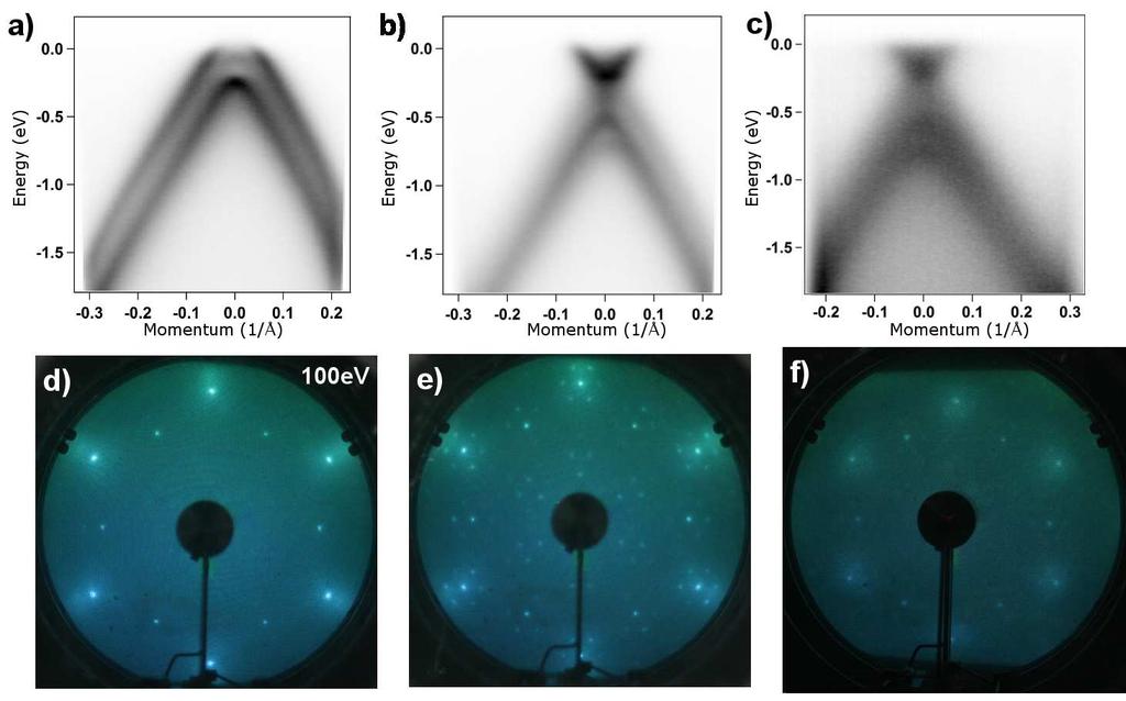
6 RESULTS ARPES and LEED of F-functionalized and pristine graphene ARPES and LEED were measured for a fluorine-functionalized, hydrogen-intercalated bilayer graphene film after insertion in the UHV analysis chamber at NSLS. The 100 C bakeout and sample entry procedure may have caused desorption of some of the fluorine, however later studies of the thermal stability of F showed that most of the F remains attached even at temperatures as high as 500 C. The ARPES spectra are intended to measure the electronic structure of the graphene, and not to quantify the effect of fluorine on the position of the Fermi level in the graphene. This is relevant in the context of ALD of Al 2 O 3 because the ALD process results in a fluorine-free Al 2 O 3 /graphene interface as well [10]. ARPES of the hydrogen intercalated film can be found in figure 2a, which shows two linear bands corresponding to the two electronic bands of bilayer graphene [16, 17]. The band structure appears unperturbed compared to pristine bilayer graphene, with the Fermi level slightly below the Dirac point (charge neutrality point), indicating a small amount of hole-doping. LEED was also measured for this sample and is shown in figure 2d. The LEED image has 6 inner spots corresponding to the first order diffraction spots from the SiC(0001), and 6 outer spots corresponding to the epitaxial bilayer graphene. The spots for both the substrate and the graphene are sharp with no evidence of rotational disorder in either material. The single set of 6 spots corresponding to graphene confirm A-B stacked graphene, as expected for growth on SiC(0001). These results suggest that the fluorine does not significantly impact the electronic or structural properties of the graphene. The bilayer graphene sample was annealed in the UHV analysis chamber at NSLS to a temperature of 1000 C. This temperature is expected to desorb all of the fluorine from the surface, as well as the intercalated hydrogen, resulting in a monolayer of graphene and a mixed sp 2 -sp 3 interfacial layer [17]. Following the anneal, ARPES and LEED were measured and are shown in Figure 2b and e, respectively. The ARPES image shows a single layer electronic structure, with a single, diffuse linear band. The Fermi level is slightly in the conduction band, indicating an electron-doped graphene film. The LEED image shows the typical ( )R30 moiré pattern found for single-layer graphene [18]. This demonstrates a return to standard epitaxial graphene on SiC(0001). 6
7 In addition to measuring a fluorine-functionalized, hydrogen-intercalated bilayer graphene sample, a single layer graphene film that was fluorine-functionalized was also measured with ARPES and LEED. Prior to measurement, the single layer film was exposed to an unfiltered photon beam from the synchrotron to correct an alignment issue with the chamber. Thus, exposure to the direct beam may have desorbed some of the fluorine functional groups prior to measurement. Therefore, figure 2c and f were measured following an 800 C anneal of the sample, to ensure that the fluorine was completely desorbed prior to measurement. The spectra show that the electronic structure of the graphene follows the typical linear dispersion expected for single layer graphene, with a small amount of electron doping indicated by the Fermi level being in the conduction band (slightly above the Dirac point). The LEED image shows the presence of the R30 moiré pattern, although the contrast is not as high as the bilayer sample after hydrogen and fluorine desorption. Surface Chemistry of TMA adsorption In addition to measuring the effect of fluorine functionalization on the electronic structure of graphene with ARPES and LEED, UHV-based TMA-dosing experiments were also carried out on similar samples. Since TMA is the most common precursor for deposition of Al 2 O 3, studying the mechanism by which fluorine-functionalization improves the quality of Al 2 O 3 films may lead to further improvements in the deposition process. In order to study the adsorption kinetics of TMA, a series of TMA-dosing experiments were first performed on three different Si substrates. Each substrate was cleaned with SC1, which is a 5:1:1 solution of deionized water, ammonium hydroxide and hydrogen peroxide, respectively. Two of the three samples then were dipped in HF to terminate the Si surface with H-atoms. Each sample was characterized with XPS using non-monochromatic X-rays (which has a much higher flux than the monochromatic source), so that trace amounts of TMA could be observed. TMA was dosed on a Si substrate that underwent a HF dip immediately prior to loading the sample into the UHV system. The H-terminated surface that resulted was found to have no TMA adsorption, as shown in Figure 3a. A second HF-dipped Si substrate underwent an in situ UHV anneal to 800 C prior to TMA dosing. The anneal (sometimes called a H flash-off) was expected to result in Si dangling bonds, which are highly reactive. Despite 7
8 the high reactivity of this surface, a similar room temperature TMA-dose did not result in any TMA adsorption (figure 3b). A SC1-cleaned Si surface was then dosed with TMA at room temperature. This resulted in significant TMA adsorption on the Si surface, as can be seen in Figure 3c. The SC1- cleaned Si is expected to have a thin (< 10 nm) oxide that is terminated in hydroxyl groups [19]. Since Al has a high affinity for bonding with O, one of the methyl groups likely reacted witht he hydrogen from an OH to form methane, with the Al(CH 3 ) 2 bonding with the surface O. This is supported by the binding energy of the Al-2p peak, which is 75 ev, indicating an oxidized Al species. Several identical doses were performed with the substrate at sequentially higher temperatures, but no additional TMA adsorbed after the initial room temperature dose. This suggests that the surface was fully saturated by the room temperature dose. The results of this preliminary work on Si-substrates indicate that TMA preferentially adsorbs on surfaces with OH or atmospheric water in the form of hydroxide. The specific surface chemistry may be more important than the overall reactivity of the surface. This result confirms previous studies, performed using different experimental techniques, suggesting that TMA generally adsorbs to oxidized surfaces [20]. TMA-dosing F-functionalized and Pristine Graphene A series of TMA-dosing experiments were performed with pristine epitaxial graphene samples and F-functionalized graphene on SiC(0001). Immediately after the graphene was grown, a high temperature UHV anneal ( 1000 C) was done on each sample to desorb the small amount of oxide that was present following the tube-furnace based graphene growth process. The oxide is presumed to result from a small amount of oxygen contamination that is present in the tube furnace during growth that oxidizes the substrate while the sample is at the growth temperature. Removal of this oxide was confirmed with XPS. The XPS measurements also showed no change in the graphene spectra. Following oxide desorption, each sample was removed from UHV and left in ambient conditions for at least one week. Prior to dosing with TMA, each sample was independently loaded into the surface analysis chamber and measured with XPS. The F-functionalized sample was placed in UHV within 30 minutes of the functionalization process. Both the pristine and F-functionalized samples were sequentially dosed with TMA at several different 8
9 temperatures, and measured with XPS after each dose. The data for both the pristine and fluorine-functionalized graphene can be found in figure 4. Survey spectra for both samples, taken prior to TMA dosing, are shown in Figure 4a. The fluorine functionalized sample has a large fluorine peak, as well as an oxygen peak that is more intense than the as-grown sample. The fluorine functionalization resulted in 7% surface coverage of fluorine, which has previously been shown to be the optimal amount of fluorine for subsequent ALD deposition of Al 2 O 3. Additional fluorine adsorption has a negative effect on device operation [10]. Both the Si-2p and C-1s spectra (not shown) lack evidence of oxide formation, and are unchanged following F-functionalization. Therefore, the oxygen is assumed to be hydroxide, caused by water adsorption on either the graphene or the SiC(0001) substrate that occurred while the sample was in ambient conditions. This has been previously confirmed by desorption of the oxygen peak following a 200 C anneal. A much higher temperature anneal would be necessary if the oxygen peak was the result of the presence of an oxide. Importantly, the fluorine-functionalization process causes increased water adsorption compared to the as-grown sample. The Al-2p spectra for the fluorine-functionalized sample, taken prior to exposure to TMA, and following sequential doses at room temperature, 500 C and 1000 C are shown in Figure 4b (see the Experimental section for details on dose geometry and amount). It can be seen that a saturation dose of TMA is achieved at room temperature, with complete thermal desorption of aluminum not occurring up to temperatures of 1000 C. This is consistent with the aluminum being in an oxidized state, since aluminum oxide is well known to be stable at very high temperatures. The small shift to higher binding energy after the 500 C anneal implies the Al is in a more oxidized state following the anneal. The final binding energy of 74.6 ev is consistent with it being oxidized. The F1s spectra can be found in Figure 4c. It can be seen that the F peak decreases following each high temperature anneal such that following the 1000 C anneal, F has completely desorbed from the surface, while both oxygen (not shown) and aluminum remain at about 2/3 of their initial concentration. An increase of TMA adsorption was not observed with the decrease of F. TMA-doses were also performed on a pristine graphene sample, which was used as a control. The XPS spectra for a room temperature dose of TMA on pristine graphene can 9
10 be found in the bottom spectra of Figure 4b. A similar temperature study was performed on the pristine graphene, and it was found that approximately 50% less TMA adsorbed on the graphene surface. It was found that for both the pristine and F-functionalized samples, saturation coverage of TMA was achieved at room temperature, similar to the preliminary studies on Si. Heating the F-functionalized graphene in the presence of TMA did not result in increased TMA adsorption, which implies that thermal desorption of fluorine is not a pre-requisite for saturation of the surface with TMA molecules. Rather, the fluorine functional groups (adsorbates) may be coordinated with adsorbed water, resulting in a surface that reacts more readily with the ALD precursors. Other functional groups may increase graphene s reactivity by a similar mechanism to enhance water adsorption. The results of peak-fitting the room temperature, TMA-dosed pristine and fluorinefunctionalized graphene are shown in Table I. It can be seen that TMA-dosing the F functionalized surface doubles the amount of Al on the surface (Table I and Figure 4b), and also doubles the amount of O found on the surface of the graphene. The increased O is likely due to atmospheric exposure of the F-functionalized sample when transferring it between the XeF 2 chamber and the surface analysis chamber where the TMA dosing and XPS were performed. Since the TMA-dosing experiments performed on Si substrates indicated that TMA preferentially adsorbs to an OH-terminated surface, these data suggest that the primary role of the F-functionalization is to increase the OH on the surface of the sample which results in additional TMA adsorption. This also supports experimental evidence that starting the ALD process with multiple water pulses improves the uniformity of the dielectric compared to starting the deposition with TMA pulses. DISCUSSION Based on the data presented in figure 3, it is clear that TMA adsorption is an extremely surface-sensitive process that relies not only on the reactivity of the surface, but also on the specific surface chemistry involved in the adsorption of the TMA molecule. Since Al has a high affinity for bonding with O, the hydroxyl-terminated surface is a thermodynamically favorable surface for the TMA to react with [20]. Since O is not present on either the H- terminated or H-flashed off surface, there is no thermodynamic driving force for the TMA 10
11 to adsorb on either surface. The results from the adsorption experiments on the Si surfaces are important in the context of graphene because they emphasize the fact that surface energy is not the only driving force for TMA adsorption. In fact, surface energy appears to be less important than providing the correct surface chemistry to encourage the TMA adsorption. This is made clear by the lack of Al on the Si surface with dangling Si bonds (highly reactive), while the hydroxyl-passivated (SC1 cleaned) Si surface was found to have Al on the surface. The ARPES data support previously published results that suggest high-quality graphenebased electronic devices can be fabricated from samples that were processed with the fluorine-functionalization process [10]. The lack of any satellite features or changes in the electronic structure from pristine graphene confirm that F-functionalization is a reversible process that negligibly affects the electronic structure of graphene. It should be noted, however, that for substantially higher fluorine doses, a change in the electronic structure would be anticipated, as has been demonstrated [13]. However, for doses previously found to optimize the deposition of Al 2 O 3 by ALD, no permanent effect has been observed. For hydrogen-intercalated graphene, following a 1000 C anneal, the LEED pattern changes significantly (Figure 2b and e). This is caused by the desorption of the intercalated hydrogen, and has been previously reported [17]. When the hydrogen desorbs, the bottom graphene layer re-bonds with the SiC(0001) substrate, forming the ( )R30 interfacial layer. This interfacial layer is partially sp 3 hybridized with the substrate, which is why the bilayer electronic structure is replaced with that of a single graphene layer [15]. In situ XPS measurements of TMA adsorption on F-functionalized graphene indicate that TMA forms a saturation coverage at room temperature. Thus, TMA does not require additional thermal energy to displace or react with fluorine atoms on the surface of the graphene. Furthermore, when additional thermal energy was provided in the presence of TMA, thermal desorption of fluorine did not increase the TMA adsorption. This suggests that the TMA adsorption on fluorine-functionalized (and ambient exposed) graphene is energetically favored, and has a small energy barrier. The role of fluorine in the TMA adsorption process can be seen in Table I. The fluorine functionalized sample has increased intensity under the O-1s peak compared to the control sample, without indication of oxide formation. Thus, the fluorine appears to attract atmospheric water to the surface of the graphene. The water provides hydroxide, which readily 11
12 reacts with TMA to encourage adsorption. In the case of performing ALD, it has been observed that starting the ALD process with multiple water pulses improves the uniformity of the dielectric on the surface of the graphene [10]. Thus the water pulses on a functionalized surface may be able to further enhance the amount and uniformity of the initial TMA adsorption compared to an un-functionalized surface. CONCLUSIONS Fluorine functionalization of graphene has been found to result in increased adsorption of TMA on the surface of graphene grown on SiC(0001). The mechanism by which the TMA adsorbs is likely related to a secondary process, by which the fluorine-functionalized graphene attracts hydroxyl groups from ambient exposure at a higher rate than pristine graphene. Additionally, ARPES measurements indicate that the fluorine functionalization process is reversible, and negligibly affects the electronic structure of the graphene. ACKNOWLEDGMENTS Work at the U.S. Naval Research Laboratory is supported by the Office of Naval Research. The NRL group and Z.R.R. acknowledge the ASEE for postdoctoral support. The SUNY Poly/UAlbany group acknowledges the support from the National Science Foundation (DMR ). The ARPES experiments were performed under the BNL grant DE-SC ZRobinso@Brockport.edu [1] F. Xia, T. Mueller, Y.-m. Lin, A. Valdes-Garcia, and P. Avouris, Nature nanotechnology 4, 839 (2009). [2] P. K. Ang, W. Chen, A. T. S. Wee, and K. P. Loh, Journal of the American Chemical Society 130, (2008). [3] L. Nyakiti, V. Wheeler, N. Garces, R. Myers-Ward, C. J. Eddy, and D. Gaskill, MRS Bulletin 37, 1149 (2012). 12
13 [4] K. V. Emtsev, A. Bostwick, K. Horn, J. Jobst, G. L. Kellogg, L. Ley, et al., Nature Materials 8, 203 (2009). [5] Y.-M. Lin, C. Dimitrakopoulos, K. A. Jenkins, D. B. Farmer, H.-Y. Chiu, A. Grill, and P. Avouris, Science 327, 662 (2010). [6] Y.-M. Lin, A. Valdes-Garcia, S.-J. Han, D. B. Farmer, I. Meric, Y. Sun, Y. Wu, C. Dimitrakopoulos, A. Grill, P. Avouris, et al., Science 332, 1294 (2011). [7] B. M. Venkatesan, D. Estrada, S. Banerjee, X. Jin, V. E. Dorgan, M.-H. Bae, N. R. Aluru, E. Pop, and R. Bashir, ACS nano 6, 441 (2011). [8] J. Moon, D. Curtis, M. Hu, D. Wong, C. McGuire, P. Campbell, et al., Electron Device Letters, IEEE 30, 650 (2009). [9] S. Kim, J. Nah, I. Jo, D. Shahrjerdi, L. Colombo, Z. Yao, E. Tutuc, and S. K. Banerjee, Applied Physics Letters 94, (2009), [10] V. Wheeler, N. Garces, L. Nyakiti, R. Myers-Ward, G. Jernigan, J. Culbertson, C. Eddy, and D. K. Gaskill, Carbon 50, 2307 (2012). [11] Y. J. Shin, Y. Wang, H. Huang, G. Kalon, A. T. S. Wee, Z. Shen, C. S. Bhatia, and H. Yang, Langmuir 26, 3798 (2010). [12] X. Wang, S. M. Tabakman, and H. Dai, Journal of the American Chemical Society 130, 8152 (2008). [13] J. T. Robinson, J. S. Burgess, C. E. Junkermeier, S. C. Badescu, T. L. Reinecke, F. K. Perkins, M. K. Zalalutdniov, J. W. Baldwin, J. C. Culbertson, P. E. Sheehan, et al., Nano letters 10, 3001 (2010). [14] J. A. Robinson, M. Hollander, M. LaBella III, K. A. Trumbull, R. Cavalero, and D. W. Snyder, Nano letters 11, 3875 (2011). [15] K. V. Emtsev, F. Speck, T. Seyller, L. Ley, and J. D. Riley, Phys. Rev. B 77, (2008). [16] T. Ohta, A. Bostwick, T. Seyller, K. Horn, and E. Rotenberg, Science 313, 951 (2006). [17] C. Riedl, C. Coletti, T. Iwasaki, A. A. Zakharov, and U. Starke, Phys. Rev. Lett. 103, (2009). [18] W. A. de Heer, C. Berger, M. Ruan, M. Sprinkle, X. Li, Y. Hu, et al., Proceedings of the National Academy of Sciences 108, (2011). [19] K. Reinhardt and W. Kern, Handbook of silicon wafer cleaning technology (William Andrew, 2008). 13
14 [20] M. M. Frank, Y. J. Chabal, and G. D. Wilk, Applied physics letters 82, 4758 (2003). 14
15 TABLE I. Table of XPS Peak Areas for F-functionalized and pristine graphene. The fluorine functionalization increases the amount of Al adsorption on the graphene surface, likely due to the increased O on the surface of the graphene. Each value is the total counts under each respective XPS peak. Sample Al O F F-func As-grown FIG. 1. Schematic of TMA-dosing system used for in situ dosing and XPS experiments. 15
16 FIG. 2. ARPES and LEED spectra of fluorine-functionalized, bilayer epitaxial graphene on SiC(0001). a) ARPES spectra for bilayer graphene and d) corresponding LEED image. b) is an ARPES image from the same sample, following a 1000 C in situ anneal that desorbed the fluorine, as well as the intercalated H2, resulting in single-layer electronic structure. e) is the corresponding LEED image, with the moire pattern confirming the single-layer structure. c) ARPES spectra for monolayer graphene and f) corresponding LEED image. 16
 HF dipped Si surface dosed with TMA following a high temperature (800 C) H flash-off to result in a highly reactive, exposed Si surface. c) SC1-cleaned Si following the TMA dose.")
17 FIG. 3. XPS survey spectra (inset is Al-2p) for a) Si surface dipped in HF prior to loading in the chamber, with no TMA adsorption following a 500L dose. b) HF dipped Si surface dosed with TMA following a high temperature (800 C) H flash-off to result in a highly reactive, exposed Si surface. c) SC1-cleaned Si following the TMA dose. The SC1 terminates the Si surface with hydroxyl groups, resulting in TMA adsorption. Neither a) nor b) resulted in TMA adsorption. 17
18 FIG. 4. XPS spectra for epitaxial graphene exposed to TMA at various temperatures: a) is the survey spectra, b) is Al2p. Saturation coverage of TMA occurred at room temperature (Area = 290), indicating thermal desorption of F is not required for TMA adsorption. The bottom profile was taken after TMA dosing pristine graphene at 25 C. c) is the F1s peak following the same anneals indicated in b). 18
19
20
21
22
Supporting Online Material for
 www.sciencemag.org/cgi/content/full/327/5966/662/dc Supporting Online Material for 00-GHz Transistors from Wafer-Scale Epitaxial Graphene Y.-M. Lin,* C. Dimitrakopoulos, K. A. Jenkins, D. B. Farmer, H.-Y.
Supporting Information
 Supporting Information Yao et al. 10.1073/pnas.1416368111 Fig. S1. In situ LEEM imaging of graphene growth via chemical vapor deposition (CVD) on Pt(111). The growth of graphene on Pt(111) via a CVD process
Wafer Scale Homogeneous Bilayer Graphene Films by. Chemical Vapor Deposition
 Supporting Information for Wafer Scale Homogeneous Bilayer Graphene Films by Chemical Vapor Deposition Seunghyun Lee, Kyunghoon Lee, Zhaohui Zhong Department of Electrical Engineering and Computer Science,
Frictional characteristics of exfoliated and epitaxial graphene
 Frictional characteristics of exfoliated and epitaxial graphene Young Jun Shin a,b, Ryan Stromberg c, Rick Nay c, Han Huang d, Andrew T. S. Wee d, Hyunsoo Yang a,b,*, Charanjit S. Bhatia a a Department
Hydrogenated Graphene
 Hydrogenated Graphene Stefan Heun NEST, Istituto Nanoscienze-CNR and Scuola Normale Superiore Pisa, Italy Outline Epitaxial Graphene Hydrogen Chemisorbed on Graphene Hydrogen-Intercalated Graphene Outline
Transport Properties of Graphene Nanoribbon Transistors on. Chemical-Vapor-Deposition Grown Wafer-Scale Graphene
 Transport Properties of Graphene Nanoribbon Transistors on Chemical-Vapor-Deposition Grown Wafer-Scale Graphene Wan Sik Hwang 1, a), Kristof Tahy 1, Xuesong Li 2, Huili (Grace) Xing 1, Alan C. Seabaugh
SUPPLEMENTARY INFORMATION
 SUPPLEMENTARY INFORMATION Towards wafer-size graphene layers by atmospheric pressure graphitization of silicon carbide Supporting online material Konstantin V. Emtsev 1, Aaron Bostwick 2, Karsten Horn
X- ray Photoelectron Spectroscopy and its application in phase- switching device study
 X- ray Photoelectron Spectroscopy and its application in phase- switching device study Xinyuan Wang A53073806 I. Background X- ray photoelectron spectroscopy is of great importance in modern chemical and
Spin and angular resolved photoemission experiments on epitaxial graphene. Abstract
 Spin and angular resolved photoemission experiments on epitaxial graphene Isabella Gierz, 1, Jan Hugo Dil, 2, 3 Fabian Meier, 2, 3 Bartosz Slomski, 2, 3 Jürg Osterwalder, 3 Jürgen Henk, 4 Roland Winkler,
Graphene devices and integration: A primer on challenges
 Graphene devices and integration: A primer on challenges Archana Venugopal (TI) 8 Nov 2016 Acknowledgments: Luigi Colombo (TI) UT Dallas and UT Austin 1 Outline Where we are Issues o Contact resistance
Optimizing Graphene Morphology on SiC(0001)
") Optimizing Graphene Morphology on SiC(0001) James B. Hannon Rudolf M. Tromp Graphene sheets Graphene sheets can be formed into 0D,1D, 2D, and 3D structures Chemically inert Intrinsically high carrier mobility
Optimizing Graphene Morphology on SiC(0001) James B. Hannon Rudolf M. Tromp Graphene sheets Graphene sheets can be formed into 0D,1D, 2D, and 3D structures Chemically inert Intrinsically high carrier mobility
Tunneling characteristics of graphene
 Tunneling characteristics of graphene Young Jun Shin, 1,2 Gopinadhan Kalon, 1,2 Jaesung Son, 1 Jae Hyun Kwon, 1,2 Jing Niu, 1 Charanjit S. Bhatia, 1 Gengchiau Liang, 1 and Hyunsoo Yang 1,2,a) 1 Department
Wide-gap Semiconducting Graphene from Nitrogen-seeded SiC
 Wide-gap Semiconducting Graphene from Nitrogen-seeded SiC F. Wang, 1 G. Liu, 2 S. Rothwell, 3 M. Nevius, 1 A. Tejeda, 4, 5 A. Taleb-Ibrahimi, 6 L.C. Feldman, 2 P.I. Cohen, 3 and E.H. Conrad 1 1 School
Epitaxial Graphene Growth on SiC Wafers. Washington, DC 20375
 Epitaxial Graphene Growth on SiC Wafers D.K. Gaskill 1, G.G. Jernigan 2, P.M. Campbell 2, J.L. Tedesco 1, J.C. Culbertson 2, B.L. VanMil 1, R.L.Myers-Ward 1, C.R. Eddy, Jr. 1 J. Moon 3, D. Curtis 3, M.
Electronic Supplementary Information. Molecular Antenna Tailored Organic Thin-film Transistor for. Sensing Application
 Electronic Supplementary Material (ESI) for Materials Horizons. This journal is The Royal Society of Chemistry 2017 Electronic Supplementary Information Molecular Antenna Tailored Organic Thin-film Transistor
XPS/UPS and EFM. Brent Gila. XPS/UPS Ryan Davies EFM Andy Gerger
 XPS/UPS and EFM Brent Gila XPS/UPS Ryan Davies EFM Andy Gerger XPS/ESCA X-ray photoelectron spectroscopy (XPS) also called Electron Spectroscopy for Chemical Analysis (ESCA) is a chemical surface analysis
Graphene Transistors for Ambipolar Mixing at Microwave Frequencies. University Park, PA 16802, USA. University Park, PA 16802, USA
 Graphene Transistors for Ambipolar Mixing at Microwave Frequencies H. Madan a, M. J. Hollander a, J. A. Robinson b and S. Datta a a Department of Electrical Engineering, The Pennsylvania State University,
Guowei He, N. Srivastava, R. M. Feenstra * Dept. Physics, Carnegie Mellon University, Pittsburgh, PA 15213
 Formation of Graphene on SiC( 0001 ) Surfaces in Disilane and Neon Environments Guowei He, N. Srivastava, R. M. Feenstra * Dept. Physics, Carnegie Mellon University, Pittsburgh, PA 15213 Abstract The formation
Ambipolar bistable switching effect of graphene
 Ambipolar bistable switching effect of graphene Young Jun Shin, 1,2 Jae Hyun Kwon, 1,2 Gopinadhan Kalon, 1,2 Kai-Tak Lam, 1 Charanjit S. Bhatia, 1 Gengchiau Liang, 1 and Hyunsoo Yang 1,2,a) 1 Department
Self-Doping Effects in Epitaxially-Grown Graphene. Abstract
 Self-Doping Effects in Epitaxially-Grown Graphene D.A.Siegel, 1,2 S.Y.Zhou, 1,2 F.ElGabaly, 3 A.V.Fedorov, 4 A.K.Schmid, 3 anda.lanzara 1,2 1 Department of Physics, University of California, Berkeley,
Supplementary Figure 1: A potential scheme to electrically gate the graphene-based metamaterial. Here density. The voltage equals, where is the DC
 Supplementary Figure 1: A potential scheme to electrically gate the graphene-based metamaterial. Here density. The voltage equals, where is the DC permittivity of the dielectric. is the surface charge
SUPPLEMENTARY INFORMATION
 DOI: 10.1038/NCHEM.2491 Experimental Realization of Two-dimensional Boron Sheets Baojie Feng 1, Jin Zhang 1, Qing Zhong 1, Wenbin Li 1, Shuai Li 1, Hui Li 1, Peng Cheng 1, Sheng Meng 1,2, Lan Chen 1 and
Supplementary Information
 Supplementary Information Supplementary Figure 1. fabrication. A schematic of the experimental setup used for graphene Supplementary Figure 2. Emission spectrum of the plasma: Negative peaks indicate an
Growth of Embedded and Protrusive Striped Graphene on 6H-SiC (0001)
") Growth of Embedded and Protrusive Striped Graphene on 6H-SiC (0001) A. Ruammaitree, H. Nakahara, K. Soda, Y. Saito Department of Quantum Engineering, Faculty of Engineering, Nagoya University, Nagoya 464-8603
Growth of Embedded and Protrusive Striped Graphene on 6H-SiC (0001) A. Ruammaitree, H. Nakahara, K. Soda, Y. Saito Department of Quantum Engineering, Faculty of Engineering, Nagoya University, Nagoya 464-8603
desorption (ESD) of the O,/Si( 111) surface K. Sakamoto *, K. Nakatsuji, H. Daimon, T. Yonezawa, S. Suga
 of the O,/Si( 111) surface K. Sakamoto *, K. Nakatsuji, H. Daimon, T. Yonezawa, S. Suga") -!!!I c%sj ELSEVIER Surface Science 306 (1994) 93-98.:.:.j:::~:::~~~::::::~:~::~~:~~,:~.~...,.. ~. :...:E.:.:: :.:.::::::~.:.:.:.:.:.:.,:.:,:,:. ~.~:+::.:.::::::j:::~::::.:...( ~ :.:.::.:.:.:,:..:,: :,,...
-!!!I c%sj ELSEVIER Surface Science 306 (1994) 93-98.:.:.j:::~:::~~~::::::~:~::~~:~~,:~.~...,.. ~. :...:E.:.:: :.:.::::::~.:.:.:.:.:.:.,:.:,:,:. ~.~:+::.:.::::::j:::~::::.:...( ~ :.:.::.:.:.:,:..:,: :,,...
Supplemental Material Chemically Resolved Interface Structure of Epitaxial Graphene on SiC(0001)
") Supplemental Material Chemically Resolved Interface Structure of Epitaxial Graphene on SiC(0001) Jonathan D. Emery 1, Blanka Detlefs 2, Hunter J. Karmel 1, Luke O. Nyakiti 3, D. Kurt Gaskill 3, Mark C.
Supplemental Material Chemically Resolved Interface Structure of Epitaxial Graphene on SiC(0001) Jonathan D. Emery 1, Blanka Detlefs 2, Hunter J. Karmel 1, Luke O. Nyakiti 3, D. Kurt Gaskill 3, Mark C.
Designing Graphene for Hydrogen Storage
 Designing Graphene for Hydrogen Storage Stefan Heun NEST, Istituto Nanoscienze-CNR and Scuola Normale Superiore Pisa, Italy Outline Introduction to Hydrogen Storage Epitaxial Graphene Hydrogen Storage
LOW-TEMPERATURE Si (111) HOMOEPITAXY AND DOPING MEDIATED BY A MONOLAYER OF Pb
 HOMOEPITAXY AND DOPING MEDIATED BY A MONOLAYER OF Pb") LOW-TEMPERATURE Si (111) HOMOEPITAXY AND DOPING MEDIATED BY A MONOLAYER OF Pb O.D. DUBON, P.G. EVANS, J.F. CHERVINSKY, F. SPAEPEN, M.J. AZIZ, and J.A. GOLOVCHENKO Division of Engineering and Applied Sciences,
LOW-TEMPERATURE Si (111) HOMOEPITAXY AND DOPING MEDIATED BY A MONOLAYER OF Pb O.D. DUBON, P.G. EVANS, J.F. CHERVINSKY, F. SPAEPEN, M.J. AZIZ, and J.A. GOLOVCHENKO Division of Engineering and Applied Sciences,
SUPPLEMENTARY INFORMATION
 In the format provided by the authors and unedited. Intrinsically patterned two-dimensional materials for selective adsorption of molecules and nanoclusters X. Lin 1,, J. C. Lu 1,, Y. Shao 1,, Y. Y. Zhang
EE 527 MICROFABRICATION. Lecture 24 Tai-Chang Chen University of Washington
 EE 527 MICROFABRICATION Lecture 24 Tai-Chang Chen University of Washington EDP ETCHING OF SILICON - 1 Ethylene Diamine Pyrocatechol Anisotropy: (100):(111) ~ 35:1 EDP is very corrosive, very carcinogenic,
Asymmetric transport efficiencies of positive and negative ion defects in amorphous ice
 Asymmetric transport efficiencies of positive and negative ion defects in amorphous ice E.-S. Moon, Y. Kim, S. Shin, H. Kang Phys. Rev. Lett. 2012, 108, 226103 Soumabha Bag CY08D021 18-08-12 Introduction:
Evidence for partial dissociation of water on flat MgO(1 0 0) surfaces
 surfaces") 6 February 2002 Chemical Physics Letters 352 (2002) 318 322 www.elsevier.com/locate/cplett Evidence for partial dissociation of water on flat MgO(1 0 0) surfaces Y.D. Kim a, R.M. Lynden-Bell b, *, A. Alavi
6 February 2002 Chemical Physics Letters 352 (2002) 318 322 www.elsevier.com/locate/cplett Evidence for partial dissociation of water on flat MgO(1 0 0) surfaces Y.D. Kim a, R.M. Lynden-Bell b, *, A. Alavi
Studying Metal to Insulator Transitions in Solids using Synchrotron Radiation-based Spectroscopies.
 PY482 Lecture. February 28 th, 2013 Studying Metal to Insulator Transitions in Solids using Synchrotron Radiation-based Spectroscopies. Kevin E. Smith Department of Physics Department of Chemistry Division
Plasma Deposition (Overview) Lecture 1
 Lecture 1") Plasma Deposition (Overview) Lecture 1 Material Processes Plasma Processing Plasma-assisted Deposition Implantation Surface Modification Development of Plasma-based processing Microelectronics needs (fabrication
Plasma Deposition (Overview) Lecture 1 Material Processes Plasma Processing Plasma-assisted Deposition Implantation Surface Modification Development of Plasma-based processing Microelectronics needs (fabrication
Table 1: Residence time (τ) in seconds for adsorbed molecules
 in seconds for adsorbed molecules") 1 Surfaces We got our first hint of the importance of surface processes in the mass spectrum of a high vacuum environment. The spectrum was dominated by water and carbon monoxide, species that represent
1 Surfaces We got our first hint of the importance of surface processes in the mass spectrum of a high vacuum environment. The spectrum was dominated by water and carbon monoxide, species that represent
Supporting Data. The University of Texas at Dallas, 800 West Campbell Road, Richardson, Texas 75080, United
 Supporting Data MoS 2 Functionalization for Ultra-thin Atomic Layer Deposited Dielectrics Angelica Azcatl, 1 Stephen McDonnell, 1 Santosh KC, 1 Xing Peng, 1 Hong Dong, 1 Xiaoye Qin, 1 Rafik Addou, 1 Greg
Water clustering on nanostructured iron oxide films
 ARTICLE Received 12 May 2013 Accepted 22 May 2014 Published 30 Jun 2014 Water clustering on nanostructured iron oxide films Lindsay R. Merte1,2, Ralf Bechstein1, W. Guowen Peng3, Felix Rieboldt1, Carrie
Plasma Etching: Atomic Scale Surface Fidelity and 2D Materials
 1 Plasma Etching: Atomic Scale Surface Fidelity and 2D Materials Thorsten Lill, Keren J. Kanarik, Samantha Tan, Meihua Shen, Alex Yoon, Eric Hudson, Yang Pan, Jeffrey Marks, Vahid Vahedi, Richard A. Gottscho
Supplementary Materials for
 www.sciencemag.org/cgi/content/full/science.1242988/dc1 Supplementary Materials for Layer-Resolved Graphene Transfer via Engineered Strain Layers Jeehwan Kim,* Hongsik Park,* James B. Hannon, Stephen W.
Supporting Information. for. Angew. Chem. Int. Ed. Z Wiley-VCH 2003
 Supporting Information for Angew. Chem. Int. Ed. Z52074 Wiley-VCH 2003 69451 Weinheim, Germany Kinetic and Thermodynamic Control via Chemical Bond Rearrangement on Si(001) Surface Chiho Hamai, Akihiko
Decoupling Graphene from SiC(0001) via Oxidation
 via Oxidation") Decoupling Graphene from SiC(0001) via Oxidation S. Oida, F.R. McFeely, J.B. Hannon, R.M. Tromp, M. Copel, Z. Chen, Y. Sun, D.B. Farmer and J. Yurkas 1 IBM Research Division, T.J. Watson Research Center,
Decoupling Graphene from SiC(0001) via Oxidation S. Oida, F.R. McFeely, J.B. Hannon, R.M. Tromp, M. Copel, Z. Chen, Y. Sun, D.B. Farmer and J. Yurkas 1 IBM Research Division, T.J. Watson Research Center,
Theory of doping graphene
 H. Pinto, R. Jones School of Physics, University of Exeter, EX4 4QL, Exeter United Kingdom May 25, 2010 Graphene Graphene is made by a single atomic layer of carbon atoms arranged in a honeycomb lattice.
Surface Transfer Doping of Diamond by Organic Molecules
 Surface Transfer Doping of Diamond by Organic Molecules Qi Dongchen Department of Physics National University of Singapore Supervisor: Prof. Andrew T. S. Wee Dr. Gao Xingyu Scope of presentation Overview
On surface synthesis of a 2D boroxine framework: a route to a novel 2D material?
 Electronic Supplementary Material (ESI) for ChemComm. This journal is The Royal Society of Chemistry 2018 On surface synthesis of a 2D boroxine framework: a route to a novel 2D material? Matus Stredansky,
Spatially resolving density-dependent screening around a single charged atom in graphene
 Supplementary Information for Spatially resolving density-dependent screening around a single charged atom in graphene Dillon Wong, Fabiano Corsetti, Yang Wang, Victor W. Brar, Hsin-Zon Tsai, Qiong Wu,
Author(s) Okuyama, H; Aruga, T; Nishijima, M. Citation PHYSICAL REVIEW LETTERS (2003), 91(
 Okuyama, H; Aruga, T; Nishijima, M. Citation PHYSICAL REVIEW LETTERS (2003), 91(") Title Vibrational characterization of the Si(111)-(7x7) Author(s) Okuyama, H; Aruga, T; Nishijima, M Citation PHYSICAL REVIEW LETTERS (2003), 91( Issue Date 2003-12-19 URL http://hdl.handle.net/2433/49840
Title Vibrational characterization of the Si(111)-(7x7) Author(s) Okuyama, H; Aruga, T; Nishijima, M Citation PHYSICAL REVIEW LETTERS (2003), 91( Issue Date 2003-12-19 URL http://hdl.handle.net/2433/49840
Supplementary Information. Atomic Layer Deposition of Platinum Catalysts on Nanowire Surfaces for Photoelectrochemical Water Reduction
 Supplementary Information Atomic Layer Deposition of Platinum Catalysts on Nanowire Surfaces for Photoelectrochemical Water Reduction Neil P. Dasgupta 1 ǂ, Chong Liu 1,2 ǂ, Sean Andrews 1,2, Fritz B. Prinz
Acidic Water Monolayer on Ruthenium(0001)
") Acidic Water Monolayer on Ruthenium(0001) Youngsoon Kim, Eui-seong Moon, Sunghwan Shin, and Heon Kang Department of Chemistry, Seoul National University, 1 Gwanak-ro, Seoul 151-747, Republic of Korea.
Acidic Water Monolayer on Ruthenium(0001) Youngsoon Kim, Eui-seong Moon, Sunghwan Shin, and Heon Kang Department of Chemistry, Seoul National University, 1 Gwanak-ro, Seoul 151-747, Republic of Korea.
Hydrogen Storage in Metalfunctionalized
 Hydrogen Storage in Metalfunctionalized Graphene Stefan Heun NEST, Istituto Nanoscienze-CNR and Scuola Normale Superiore Pisa, Italy Outline Introduction to Hydrogen Storage Epitaxial Graphene Hydrogen
Energy Spectroscopy. Ex.: Fe/MgO
 Energy Spectroscopy Spectroscopy gives access to the electronic properties (and thus chemistry, magnetism,..) of the investigated system with thickness dependence Ex.: Fe/MgO Fe O Mg Control of the oxidation
Segregated chemistry and structure on (001) and (100) surfaces of
 and (100) surfaces of") Supporting Information Segregated chemistry and structure on (001) and (100) surfaces of (La 1-x Sr x ) 2 CoO 4 override the crystal anisotropy in oxygen exchange kinetics Yan Chen a, Helena Téllez b,c,
Supporting Information Segregated chemistry and structure on (001) and (100) surfaces of (La 1-x Sr x ) 2 CoO 4 override the crystal anisotropy in oxygen exchange kinetics Yan Chen a, Helena Téllez b,c,
Effect of Oxygen Adsorption on the Local Properties of Epitaxial Graphene on SiC (0001)
") Effect of Oxygen Adsorption on the Local Properties of Epitaxial Graphene on SiC (0001) C. Mathieu 1, B. Lalmi 2, T. O. Mentes 3, E. Pallecchi 1, A. Locatelli 3, S. Latil 4, R. Belkhou 2 and A. Ouerghi
Effect of Oxygen Adsorption on the Local Properties of Epitaxial Graphene on SiC (0001) C. Mathieu 1, B. Lalmi 2, T. O. Mentes 3, E. Pallecchi 1, A. Locatelli 3, S. Latil 4, R. Belkhou 2 and A. Ouerghi
Direct Measurement of Adhesion Energy of Monolayer Graphene As-Grown. on Copper and Its Application to Renewable Transfer Process
 SUPPORTING INFORMATION Direct Measurement of Adhesion Energy of Monolayer Graphene As-Grown on Copper and Its Application to Renewable Transfer Process Taeshik Yoon 1, Woo Cheol Shin 2, Taek Yong Kim 2,
XPS Depth Profiling of Epitaxial Graphene Intercalated with FeCl 3
 XPS Depth Profiling of Epitaxial Graphene Intercalated with FeCl 3 Mahdi Ibrahim Maynard H. Jackson High School Atlanta, GA. Faculty Advisor: Dr. Kristin Shepperd Research Group: Prof. Edward Conrad School
Supporting Information. Effects of Environmental Water Absorption by. Film Transistor Performance and Mobility
 Supporting Information Effects of Environmental Water Absorption by Solution-Deposited Al 2 O 3 Gate Dielectrics on Thin Film Transistor Performance and Mobility Trey B. Daunis, James M. H. Tran, and Julia
Special Properties of Au Nanoparticles
 Special Properties of Au Nanoparticles Maryam Ebrahimi Chem 7500/750 March 28 th, 2007 1 Outline Introduction The importance of unexpected electronic, geometric, and chemical properties of nanoparticles
Outlines 3/12/2011. Vacuum Chamber. Inside the sample chamber. Nano-manipulator. Focused ion beam instrument. 1. Other components of FIB instrument
 Focused ion beam instruments Outlines 1. Other components of FIB instrument 1.a Vacuum chamber 1.b Nanomanipulator 1.c Gas supply for deposition 1.d Detectors 2. Capabilities of FIB instrument Lee Chow
An account of our efforts towards air quality monitoring in epitaxial graphene on SiC
 European Network on New Sensing Technologies for Air Pollution Control and Environmental Sustainability - EuNetAir COST Action TD1105 2 nd International Workshop EuNetAir on New Sensing Technologies for
PHI 5000 Versaprobe-II Focus X-ray Photo-electron Spectroscopy
 PHI 5000 Versaprobe-II Focus X-ray Photo-electron Spectroscopy The very basic theory of XPS XPS theroy Surface Analysis Ultra High Vacuum (UHV) XPS Theory XPS = X-ray Photo-electron Spectroscopy X-ray
Surface Chemistry and Reaction Dynamics of Electron Beam Induced Deposition Processes
 Surface Chemistry and Reaction Dynamics of Electron Beam Induced Deposition Processes e -? 2 nd FEBIP Workshop Thun, Switzerland 2008 Howard Fairbrother Johns Hopkins University Baltimore, MD, USA Outline
Supplementary Figure S1. AFM images of GraNRs grown with standard growth process. Each of these pictures show GraNRs prepared independently,
 Supplementary Figure S1. AFM images of GraNRs grown with standard growth process. Each of these pictures show GraNRs prepared independently, suggesting that the results is reproducible. Supplementary Figure
Atomic layer deposition of titanium nitride
 Atomic layer deposition of titanium nitride Jue Yue,version4, 04/26/2015 Introduction Titanium nitride is a hard and metallic material which has found many applications, e.g.as a wear resistant coating[1],
EE 527 MICROFABRICATION. Lecture 25 Tai-Chang Chen University of Washington
 EE 527 MICROFABRICATION Lecture 25 Tai-Chang Chen University of Washington ION MILLING SYSTEM Kaufmann source Use e-beam to strike plasma A magnetic field applied to increase ion density Drawback Low etch
SUPPLEMENTARY INFORMATION. Observation of tunable electrical bandgap in large-area twisted bilayer graphene synthesized by chemical vapor deposition
 SUPPLEMENTARY INFORMATION Observation of tunable electrical bandgap in large-area twisted bilayer graphene synthesized by chemical vapor deposition Jing-Bo Liu 1 *, Ping-Jian Li 1 *, Yuan-Fu Chen 1, Ze-Gao
SUPPLEMENTARY INFORMATION
 SUPPLEMENTARY INFORMATION Facile Synthesis of High Quality Graphene Nanoribbons Liying Jiao, Xinran Wang, Georgi Diankov, Hailiang Wang & Hongjie Dai* Supplementary Information 1. Photograph of graphene
NanoEngineering of Hybrid Carbon Nanotube Metal Composite Materials for Hydrogen Storage Anders Nilsson
 NanoEngineering of Hybrid Carbon Nanotube Metal Composite Materials for Hydrogen Storage Anders Nilsson Stanford Synchrotron Radiation Laboratory (SSRL) and Stockholm University Coworkers and Ackowledgement
Vapor Phase Doping with N-type Dopant into Silicon by Atmospheric Pressure Chemical Vapor Deposition
 495 10.1149/1.2986806 The Electrochemical Society Vapor Phase Doping with N-type Dopant into Silicon by Atmospheric Pressure Chemical Vapor Deposition Shotaro Takeuchi, Ngoc Duy Nguyen, Frederik Leys,
TPD-MS. Photocatalytic Studies Using Temperature Programmed Desorption Mass Spectrometry (TPD-MS) APPLICATION NOTE NOTE
 APPLICATION NOTE NOTE") TPD-MS APPLICATION NOTE NOTE Photocatalytic Studies Using Temperature Programmed Desorption Mass Spectrometry (TPD-MS) Thermal analysis consists of many techniques for the exploration of the physical properties
TPD-MS APPLICATION NOTE NOTE Photocatalytic Studies Using Temperature Programmed Desorption Mass Spectrometry (TPD-MS) Thermal analysis consists of many techniques for the exploration of the physical properties
Formation of a Buffer Layer for Graphene on C-Face SiC{0001}
 Journal of ELECTRONIC MATERIALS, Vol. 43, No. 4, 2014 DOI: 10.1007/s11664-013-2901-8 Ó 2013 TMS Formation of a Buffer Layer for Graphene on C-Face SiC{0001} GUOWEI HE, 1 N. SRIVASTAVA, 1 and R.M. FEENSTRA
Atmospheric pressure graphitization of SiC(0001) A route towards wafer-size graphene layers
 A route towards wafer-size graphene layers") Atmospheric pressure graphitization of SiC(000) A route towards wafer-size graphene layers Konstantin V. Emtsev, Aaron Bostwick, Karsten Horn 3, Johannes Jobst 4, Gary L. Kellogg 5, Lothar Ley, Jessica
Atmospheric pressure graphitization of SiC(000) A route towards wafer-size graphene layers Konstantin V. Emtsev, Aaron Bostwick, Karsten Horn 3, Johannes Jobst 4, Gary L. Kellogg 5, Lothar Ley, Jessica
Interaction of Hydrogen on a Lanthanum hexaboride (111) Surface Jenna Cameli, Aashani Tillekaratne, Michael Trenary Department of Chemistry,
 Surface Jenna Cameli, Aashani Tillekaratne, Michael Trenary Department of Chemistry,") Interaction of Hydrogen on a Lanthanum hexaboride (111) Surface Jenna Cameli, Aashani Tillekaratne, Michael Trenary Department of Chemistry, University of Illinois at Chicago, Chicago, IL 60607 1 Abstract
Interaction of Hydrogen on a Lanthanum hexaboride (111) Surface Jenna Cameli, Aashani Tillekaratne, Michael Trenary Department of Chemistry, University of Illinois at Chicago, Chicago, IL 60607 1 Abstract
SUPPLEMENTARY INFORMATION
 Engineered doping of organic semiconductors for enhanced thermoelectric efficiency G.-H. Kim, 1 L. Shao, 1 K. Zhang, 1 and K. P. Pipe 1,2,* 1 Department of Mechanical Engineering, University of Michigan,
SUPPLEMENTARY INFORMATION
 doi:.38/nature09979 I. Graphene material growth and transistor fabrication Top-gated graphene RF transistors were fabricated based on chemical vapor deposition (CVD) grown graphene on copper (Cu). Cu foil
Supporting Information. by Hexagonal Boron Nitride
 Supporting Information High Velocity Saturation in Graphene Encapsulated by Hexagonal Boron Nitride Megan A. Yamoah 1,2,, Wenmin Yang 1,3, Eric Pop 4,5,6, David Goldhaber-Gordon 1 * 1 Department of Physics,
Lecture 6 Plasmas. Chapters 10 &16 Wolf and Tauber. ECE611 / CHE611 Electronic Materials Processing Fall John Labram 1/68
 Lecture 6 Plasmas Chapters 10 &16 Wolf and Tauber 1/68 Announcements Homework: Homework will be returned to you on Thursday (12 th October). Solutions will be also posted online on Thursday (12 th October)
Atomic Level Analysis of SiC Devices Using Numerical Simulation
 Atomic Level Analysis of Devices Using Numerical mulation HIRSE, Takayuki MRI, Daisuke TERA, Yutaka ABSTRAT Research and development of power semiconductor devices with (silicon carbide) has been very
Improved Interfacial and Electrical Properties of GaSb Metal Oxide
 Improved Interfacial and Electrical Properties of GaSb Metal Oxide Semiconductor Devices Passivated with Acidic (NH 4 ) 2 S Solution Lianfeng Zhao, Zhen Tan, Jing Wang, and Jun Xu * Tsinghua National Laboratory
Reaction Mechanism of Area-Selective Atomic
 Supporting Information Reaction Mechanism of Area-Selective Atomic Layer Deposition for Al 2 O 3 Nanopatterns Seunggi Seo 1, Il-Kwon Oh 1, Byung Chul Yeo 1, 2, Sang Soo Han 2, Chang Mo Yoon 1, JOON YOUNG
JOHN G. EKERDT RESEARCH FOCUS
 JOHN G. EKERDT RESEARCH FOCUS We study the surface, growth and materials chemistry of metal, dielectric, ferroelectric, and polymer thin films. We seek to understand and describe nucleation and growth
Growth of Graphene Architectures on SiC
 Wright State University CORE Scholar Special Session 5: Carbon and Oxide Based Nanostructured Materials (2012) Special Session 5 6-2012 Growth of Graphene Architectures on SiC John J. Boeckl Weijie Lu
Supplementary Information
 Supplementary Information Plasma-assisted reduction of graphene oxide at low temperature and atmospheric pressure for flexible conductor applications Seung Whan Lee 1, Cecilia Mattevi 2, Manish Chhowalla
Pb thin films on Si(111): Local density of states and defects
: Local density of states and defects") University of Wollongong Research Online Australian Institute for Innovative Materials - Papers Australian Institute for Innovative Materials 2014 Pb thin films on Si(111): Local density of states and
University of Wollongong Research Online Australian Institute for Innovative Materials - Papers Australian Institute for Innovative Materials 2014 Pb thin films on Si(111): Local density of states and
Characterization of Hydrogenated Graphene on Copper. Research Thesis. Presented in Partial Fulfillment of the Requirements for graduation
 Characterization of Hydrogenated Graphene on Copper Research Thesis Presented in Partial Fulfillment of the Requirements for graduation with Research Distinction in Physics in the undergraduate colleges
SUPPORTING INFORMATION: Titanium Contacts to Graphene: Process-Induced Variability in Electronic and Thermal Transport
 SUPPORTING INFORMATION: Titanium Contacts to Graphene: Process-Induced Variability in Electronic and Thermal Transport Keren M. Freedy 1, Ashutosh Giri 2, Brian M. Foley 2, Matthew R. Barone 1, Patrick
Thermal reactions on the Cl-terminated SiGe(1 0 0) surface
 surface") Surface Science 507 510 (2002) 295 299 www.elsevier.com/locate/susc Thermal reactions on the Cl-terminated SiGe(1 0 0) surface Meng-Wen Wu a, Shiang-Yuan Pan a, Wei-Hsiu Hung b, Deng-Sung Lin a, * a Institute
Surface Science 507 510 (2002) 295 299 www.elsevier.com/locate/susc Thermal reactions on the Cl-terminated SiGe(1 0 0) surface Meng-Wen Wu a, Shiang-Yuan Pan a, Wei-Hsiu Hung b, Deng-Sung Lin a, * a Institute
Epitaxial graphene on SiC formed by the surface structure control technique
 Epitaxial graphene on SiC formed by the surface structure control technique Takuya Aritsuki*, Takeshi Nakashima, Keisuke Kobayashi, Yasuhide Ohno, and Masao Nagase Tokushima University, Tokushima 770-8506,
EE C245 ME C218 Introduction to MEMS Design Fall 2007
 EE C245 ME C218 Introduction to MEMS Design Fall 2007 Prof. Clark T.-C. Nguyen Dept. of Electrical Engineering & Computer Sciences University of California at Berkeley Berkeley, CA 94720 Lecture 5: ALD,
The effectiveness of HCl and HF cleaning of Si 0.85 Ge 0.15 surface. Stanford Synchrotron Radiation Lab, Menlo Park, CA 94025
 July 2008 SLAC-PUB-13302 The effectiveness of HCl and HF cleaning of Si 0.85 Ge 0.15 surface Yun Sun, a) Zhi Liu, Shiyu Sun, Piero Pianetta Stanford Synchrotron Radiation Lab, Menlo Park, CA 94025 The
Hydrogenation of Single Walled Carbon Nanotubes
 Hydrogenation of Single Walled Carbon Nanotubes Anders Nilsson Stanford Synchrotron Radiation Laboratory (SSRL) and Stockholm University Coworkers and Ackowledgement A. Nikitin 1), H. Ogasawara 1), D.
LECTURE 5 SUMMARY OF KEY IDEAS
 LECTURE 5 SUMMARY OF KEY IDEAS Etching is a processing step following lithography: it transfers a circuit image from the photoresist to materials form which devices are made or to hard masking or sacrificial
Controlling Graphene Ultrafast Hot Carrier Response from Metal-like. to Semiconductor-like by Electrostatic Gating
 Controlling Graphene Ultrafast Hot Carrier Response from Metal-like to Semiconductor-like by Electrostatic Gating S.-F. Shi, 1,2* T.-T. Tang, 1 B. Zeng, 1 L. Ju, 1 Q. Zhou, 1 A. Zettl, 1,2,3 F. Wang 1,2,3
Supplementary Figure 1 Experimental setup for crystal growth. Schematic drawing of the experimental setup for C 8 -BTBT crystal growth.
 Supplementary Figure 1 Experimental setup for crystal growth. Schematic drawing of the experimental setup for C 8 -BTBT crystal growth. Supplementary Figure 2 AFM study of the C 8 -BTBT crystal growth
Graphene films on silicon carbide (SiC) wafers supplied by Nitride Crystals, Inc.
 wafers supplied by Nitride Crystals, Inc.") 9702 Gayton Road, Suite 320, Richmond, VA 23238, USA Phone: +1 (804) 709-6696 info@nitride-crystals.com www.nitride-crystals.com Graphene films on silicon carbide (SiC) wafers supplied by Nitride Crystals,
9702 Gayton Road, Suite 320, Richmond, VA 23238, USA Phone: +1 (804) 709-6696 info@nitride-crystals.com www.nitride-crystals.com Graphene films on silicon carbide (SiC) wafers supplied by Nitride Crystals,
Oxygen Incorporation in Rubrene Single Crystals
 Oxygen Incorporation in Rubrene Single Crystals Daniel D. T. Mastrogiovanni 1, Jeff Mayer 2, Alan S. Wan 2, Aleksey Vishnyakov 3, Alexander V. Neimark 3, Vitaly Podzorov 4,5, Leonard C. Feldman 4,5, and
ConceptGraphene. Small or medium-scale focused research project. WP2 Characterization and integration
 ConceptGraphene New Electronics Concept: Wafer-Scale Epitaxial Graphene Small or medium-scale focused research project WP2 Characterization and integration Deliverable 2.2 Report on the influence of environment
Electronic Supplementary Information
 Electronic Supplementary Material (ESI) for Chemical Science. This journal is The Royal Society of Chemistry 218 Rel. intensity Rel. intensity Electronic Supplementary Information Under-cover stabilization
S1. X-ray photoelectron spectroscopy (XPS) survey spectrum of
 survey spectrum of") Site-selective local fluorination of graphene induced by focused ion beam irradiation Hu Li 1, Lakshya Daukiya 2, Soumyajyoti Haldar 3, Andreas Lindblad 4, Biplab Sanyal 3, Olle Eriksson 3, Dominique Aubel
Site-selective local fluorination of graphene induced by focused ion beam irradiation Hu Li 1, Lakshya Daukiya 2, Soumyajyoti Haldar 3, Andreas Lindblad 4, Biplab Sanyal 3, Olle Eriksson 3, Dominique Aubel
Extreme band bending at MBE-grown InAs(0 0 1) surfaces induced by in situ sulphur passivation
 surfaces induced by in situ sulphur passivation") Journal of Crystal Growth 237 239 (2002) 196 200 Extreme band bending at MBE-grown InAs(0 0 1) surfaces induced by in situ sulphur passivation M.J. Lowe a, T.D. Veal a, C.F. McConville a, G.R. Bell b,
Journal of Crystal Growth 237 239 (2002) 196 200 Extreme band bending at MBE-grown InAs(0 0 1) surfaces induced by in situ sulphur passivation M.J. Lowe a, T.D. Veal a, C.F. McConville a, G.R. Bell b,
Fabrication Technology, Part I
 EEL5225: Principles of MEMS Transducers (Fall 2004) Fabrication Technology, Part I Agenda: Microfabrication Overview Basic semiconductor devices Materials Key processes Oxidation Thin-film Deposition Reading:
Supporting Information for: Capacitive Sensing of Intercalated H2O Molecules Using Graphene
 Supporting Information for: Capacitive Sensing of Intercalated H2O Molecules Using Graphene Eric J. Olson, Rui Ma, Tao Sun, Mona A. Ebrish, Nazila Haratipour, Kyoungmin Min, Narayana R. Aluru, and Steven