Lecture Note #13. Bard, ch. 18. Photoelectrochemistry (ch. 18) 1. Electrogenerated Chemiluminescence 2. Photoelectrochemistry at Semiconductors
|
|
|
- Edgar Bell
- 5 years ago
- Views:
Transcription
1 Lecture Note #13 Photoelectrochemistry (ch. 18) 1. Electrogenerated Chemiluminescence 2. Photoelectrochemistry at Semiconductors Bard, ch. 18
2 Photoelectrochemistry Radiation energy electrical or chemical energy e.g., ECL, electrochromic device, EL, sensors General Concepts of luminescence the type of excitation - Photoluminescence: light emission by UV or visible light - Radioluminescence (scintillation): excited by radioactive substances - Cathodoluminescence: excited by high velocity electron bombardment - X-ray luminescence: by X-rays - Chemiluminescence: by chemical reactions -Electrochemiluminescence or electrogenerated chemiluminescence: by electrochemical reactions - Electroluminescence: by electric voltage Luminescent materials (or luminophors): substances which exhibit luminescence - organic (organoluminophors) - inorganic (phosphors)
3 Electrochemiluminescence (or electrogenerated chemiluminescence, ECL) solution phase chemiluminescence resulting from electron transfer reactions, often involving aromatic radical ions general reaction mechanisms - S route: energy sufficient (energy released by the electron transfer process is sufficient to raise a product to the emitting state) - T route: energy deficient (the energy available in electron transfer is substantially less than that required to reach the emitting state), triplet intermediates
4
5
6 experimental techniques
7 ECL at semiconductors
8 ECL in Pyrene (Py) and TMPD solution: 400 nm & 450 nm (a) ECL (b) Fluorescence (excitation at 350 nm)
9 Analytical applications of ECL Light intensity is proportional to concentration analysis using ECL -Very sensitive: very low light level -No light source is needed: electrochemical excitation Most frequently used ECL-active label: Ru(bpy) 3 2+

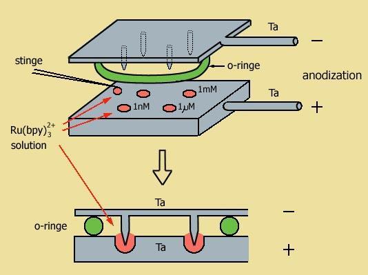
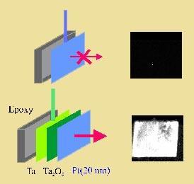
10 Electro(chemi)luminescent Devices Ru 계화합물의농도에따른발광특성 Pt 나노박막이덮힌 Ta 2 O 5 의발광특성
11 In-situ transmittance test Power meter Potentiostat Detector Electrochemical cell or EC devices He-Ne laser (633nm)
12 Photoelectrochemistry at semiconductors Radiation energy electrical or chemical energy photoelectrochemical system: absorption of light by the system (e.g., sun light) chemical reactions & flow of current semiconductor: absorb photons electron-hole pairs oxidation/reduction reactions products (photocurrent)
13 - Hydrogen fuel production (H + or H 2 O reduction): i) kinetically difficult catalyst, ii) recombining electrons and holes and lowering the efficiency of the photoreaction unless rapid chemical reaction 2H + + Red H 2 + Ox Red: sacrificial (electron) donor e.g., Photoproduction of H 2 on p-gaas with methyl viologen & colloidal Pt (J. Am. Chem. Soc., 102, 1488 (1980))
14 Very slow H 2 photoreaction on GaAs (high hydrogen overpotential) fast reaction of MV 2+/1+ + Pt (fast hydrogen evolution) viologen + polymer/self assembly etc e.g., CdS particles in Nafion
15 General photoelectrochemical system for conversion of solar energy(sunlight) to useful chemical products Ox + Red + h Red + Ox e.g., H 2 O 2H 2 + O 2 or H 2, Cl 2, OH - from NaCl solution
16
17 Energy transduction step 1) adsorption of a photon of incident light & conversion to an electron-hole pair (e - h + ) 2) electron & hole react with relays or mediators (serve the role of capturing e - & h +, thereby preventing the backreaction (recombination of e - & h + to produce heat)) 3) conducting these charges to catalyst centers where the final reactions occur
18 Semiconductor electrodes Band model
19 intrinsic semiconductor; undoped
20 - intrinsic semiconductor; # of e - (n i ) & h + (p i ) per cm 3 at T Where T(K), m n, m p ; reduced masses of e - & h +, m e*, m h* ; relative effective masses where m e* = m n /m 0, m h* = m p /m 0 (m 0 ; rest mass of an electron) n i = p i ~ 2.5 x exp(-e g /2kT) cm -3 (near 25ºC) For Si, n i = p i ~ 1.4 x cm -3 E g > 1.5 ev few carriers: electrical insulators
21
22 - Mobilities (, cm 2 V -1 s -1 ) vs. diffusion coefficient (cm 2 s -1 ) D i = kt i = at 25 C, i = n, p
23 Extrinsic semiconductors; doped - dopants or impurity; ~ppm, typical donor densities (N D ) are cm -3 n-type p-type
24 Extrinsic semiconductors; doped - dopants or impurity; ~ppm, typical donor densities (N D ) are cm -3
25 n-type: total density (n) of electrons in CB n = p + N D, p; hole density (thermal activation of VB atoms) most cases for moderate doping N D >> p, n ~ N D For any materials (intrinsic or extrinsic) For n-type SC e.g., cm -3 As doped Si electron density ~10 17 cm -3, hole density ~ 460 majority carrier: electron
26 p-type dopant (acceptor) density; N A, electron density (by thermal promotion); n total density of holes (p) p = n + N A when N A >> n, p = N A hole; majority carriers n = n i2 /N A e.g., Si: N A = 5 x acceptor/cm 3, n ~ 4000 cm -3 compound semiconductor (e.g., GaAs or TiO 2 ); n-type or p-type replacement of impurity atoms to the constituent lattice atoms, impurity atoms in an interstitial position, lattice vacancy or broken bond e.g., n-tio 2 : oxygen vacancies in the lattice
27 extrinsic SC; E F move up & down depending upon doping e.g., cm -3 As doped Si N D ~10 17 cm -3, N C = 2.8 x cm -3, 25 C E F = E C (25.7 x 10⁻³ ev) ln(n C /N D ) ~ E C 0.13 ev - if N D < N C, N A < N V SC - if higher doping levels; Fermi level moves into VB or CB show metallic conductivity e.g., transparent SnO 2 (E g = 3.5 ev) + heavily doping with Sb(III) (N D > cm -3 ) the material becomes conductive
28 Fermi level 1) probability that an electronic level at energy E is occupied by an electron at thermal equilibrium f(e) Fermi-Dirac distribution function - Fermi level E F ; value of E for which f(e) = 1/2 (equally probable that a level is occupied or vacant) - At T = 0, all levels below E F (E < E F ) are occupied (f(e) 1); all levels E > E F vacant -intrinsic SC: E F in the middle of CB and VB edges
29 2) alternative definition of E F for a phase : electrochemical potential - useful in thermodynamic considerations of reactions and interfaces; at equilibrium electrically, the electrochemical potential of electrons in all phases must be same by charge transfer same Fermi level - Fermi levels difference between two phases; function of the applied potential Fermi level (uncharged phase) vs. work function ( ) = -E F
30 Semiconductor/solution interface electron transfer at the interface (same principles as those given above) + chemical reaction (if possible, e.g., decomposition of SC, oxide film formation) complicate - Si; SiO 2 (if oxygen or oxidant in solution); hinder electron transfer The distribution of charge (e - /h + in SC & ions in solution) and potential; depend on their relative Fermi level Fermi level in solution: electrochemical potential of electrons in solution phase ( ) - governed by the nature and concentration of the redox species present in the solution and is directly related to the solution redox potential as calculated by the Nernst equation - at the point of zero charge, no surface state, no specifically adsorbed ions, no excess charge the distribution of carriers (e -, h +, anions, cations) is uniform from surface to bulk, and the energy bands are flat flat band potential (E fb ) ; no space charge layer in SC & no diffuse layer in solution
31 n-type
32 potential difference (by applied voltage or Fermi level difference) ; charged interface space charge layer (thickness W); potential difference V, dopant density N D 50 ~ 2000 Å band bending: because of non uniform carrier density in SC (upward (with respect to the bulk SC) for a positively charged SC and downward for a negatively charged one) electric field in the space charge region direction of motion
33 The capacitance of the space charge layer Mott-Schottky plot Mott-Schottky plot: useful in characterizing SC/liquid interface where a plot of (1/C SC2 ) vs. E should be linear values of E fb and N D from the intercept and slope
34 space charge capacitance C sc Mott-Schottly equation 1/C sc2 = (2/e 0 N) 1/2 (- - kt/e) : dielectric constant, N: donor or acceptor densities, e: quantity of charge, - = E-E fb A plot of 1/C sc2 vs. potential E should be linear E fb, doping level N Mott-Schottky plots for n- and p-type InP in 1 M KCl M HCl
35 Photoeffects at semiconductor electrodes 1: dark 2: irradiation 3: Pt electrode n-type p-type
36 p-type
37 Photoelectrochemical cells Photovoltaic cells: convert light to electricity Photoelectrosynthetic cells: Radiant E to chemical energy Photocatalytic cells: Light E to overcome activation E of the process
38 Band gap vs. wavelength limit to utilize sunlight (e.g., TiO 2 (3.0 ev)) dye sensitization of a semiconductor

39
40 Potential vs. energy (vs. vacuum)
41 Photoelectrochemical photovoltaic cells basic idea - SC & counter electrodes in the same solution containing the redox couple D/D + - no net chemical reaction occurs in the solution during irradiation; hole oxidize D to D + & electrons reduce D + to D - net effect: conversion of the radiant energy to electrical energy (h + and e - ) in the external circuit connecting the two electrodes Conversion efficiency depends on the quantum efficiency of the carrier generation, the rates of interfacial electron transfer, the rate of carrier recombination, internal cell resistance
42 - Photoelectrochemical photovoltaic cells
43 photoactive dyes adsorbed or covalently attached to the electrode surface - to sensitize the electrode to visible light and produce photocurrents under irradiation with light of smaller energy than that corrsponding to the SC band gap - principle: absorption of light in the dye layer (smaller energy than SC band gap) injection of electrons to CB of SC; hole in dye filled by electron transfer from solution species (R to O)
44 e.g., liquid junction photovoltaic cell dye sensitized SC: TiO 2
45 Particulate SC systems e.g., solar energy to produce fuels or to remove pollutants from water principles - behave as microelectrode: carry out both anodic and cathodic half-reactions at different sites on the particle surface e.g., TiO 2 particle: CN - oxidation by O 2 (CN - oxidation + O 2 reduction) by e - h + pair
46 -particle dimensions < space charge layer ; charge separation by electric charge does not play a major role in promoting e - -h + separation - trapping of charge at surface state maybe important in charge separation supported SC particles - why? Prevent the flocculation & settling out of very small particles - if transparent support: high area thin films & small SC particle - support materials polymer films or membranes: e.g., Nafion with Cd 2+ /H 2 S (CdS) Inorganics (SiO 2, clays, zeolites) Organic supports: micelles, langmuir-blodgett film with CdS
47 Multijunction photoelectrochemical systems - limited single junction: splitting of water (< 0.8 V open circuit photovoltage), p/n junction Si (~o.55 V), electric eel (one organ; 0.1 V in series, 500 V) - e.g., Texas Instrument Solar Energy System
48 Small (250 ) Si spheres (n-si coated p-si & p-si coated n-si)/glass matrix + catalyst; irradiation of the p/n junction produce 1.1 V decompose HBr to H 2 + Br 2 ; other part; H 2 + Br 2 produce electricity - CdSe/Ti/CoS
49 Nano(or quantum, Q-) particles size quantization effect in Q-particles - particle size sufficiently small: electronic properties differ from that of bulk material - quantom dot, quantum wire, quantum particle - nano thickness layers: superlattices (different materials sandwiched) band energetics of Q-particles - increase band gap - CB up and VB down: electrons are better reductants & holes are better oxidants in Q-particles e.g., enhanced photoredox chemistry at smaller particles of PbSe and HgSe
50 Semiconductor particles Grains Nanocrystalline films Quantum particles (Q-particles or quantum dots)
Chemistry Instrumental Analysis Lecture 8. Chem 4631
 Chemistry 4631 Instrumental Analysis Lecture 8 UV to IR Components of Optical Basic components of spectroscopic instruments: stable source of radiant energy transparent container to hold sample device
e - Galvanic Cell 1. Voltage Sources 1.1 Polymer Electrolyte Membrane (PEM) Fuel Cell
 Fuel Cell") Galvanic cells convert different forms of energy (chemical fuel, sunlight, mechanical pressure, etc.) into electrical energy and heat. In this lecture, we are interested in some examples of galvanic cells.
Galvanic cells convert different forms of energy (chemical fuel, sunlight, mechanical pressure, etc.) into electrical energy and heat. In this lecture, we are interested in some examples of galvanic cells.
Electrochemistry of Semiconductors
 Electrochemistry of Semiconductors Adrian W. Bott, Ph.D. Bioanalytical Systems, Inc. 2701 Kent Avenue West Lafayette, IN 47906-1382 This article is an introduction to the electrochemical properties of
Solar Cell Materials and Device Characterization
 Solar Cell Materials and Device Characterization April 3, 2012 The University of Toledo, Department of Physics and Astronomy SSARE, PVIC Principles and Varieties of Solar Energy (PHYS 4400) and Fundamentals
Laurea in Scienza dei Materiali Materiali Inorganici Funzionali. Hydrogen production by photocatalytic water splitting
 Laurea in Scienza dei Materiali Materiali Inorganici Funzionali Hydrogen production by photocatalytic water splitting Prof. Dr. Antonella Glisenti -- Dip. Scienze Chimiche -- Università degli Studi di
Electrons are shared in covalent bonds between atoms of Si. A bound electron has the lowest energy state.
 Photovoltaics Basic Steps the generation of light-generated carriers; the collection of the light-generated carriers to generate a current; the generation of a large voltage across the solar cell; and
Mesoporous titanium dioxide electrolyte bulk heterojunction
 Mesoporous titanium dioxide electrolyte bulk heterojunction The term "bulk heterojunction" is used to describe a heterojunction composed of two different materials acting as electron- and a hole- transporters,
Electron Energy, E E = 0. Free electron. 3s Band 2p Band Overlapping energy bands. 3p 3s 2p 2s. 2s Band. Electrons. 1s ATOM SOLID.
 Electron Energy, E Free electron Vacuum level 3p 3s 2p 2s 2s Band 3s Band 2p Band Overlapping energy bands Electrons E = 0 1s ATOM 1s SOLID In a metal the various energy bands overlap to give a single
SEMICONDUCTORS AS CATALYSTS FOR WATER SPLITTING. Chandramathy Surendran Praveen. Materials Research Laboratory UNIVERSITY OF NOVA GORICA
 SEMICONDUCTORS AS CATALYSTS FOR WATER SPLITTING Chandramathy Surendran Praveen Materials Research Laboratory UNIVERSITY OF NOVA GORICA OUTLINE Introduction and history of the discovery of semiconductor
Monolithic Cells for Solar Fuels
 Electronic Supplementary Material (ESI) for Chemical Society Reviews. This journal is The Royal Society of Chemistry 2014 Monolithic Cells for Solar Fuels Jan Rongé, Tom Bosserez, David Martel, Carlo Nervi,
ELEMENTARY BAND THEORY
 ELEMENTARY BAND THEORY PHYSICIST Solid state band Valence band, VB Conduction band, CB Fermi energy, E F Bloch orbital, delocalized n-doping p-doping Band gap, E g Direct band gap Indirect band gap Phonon
Electrons, Holes, and Defect ionization
 Electrons, Holes, and Defect ionization The process of forming intrinsic electron-hole pairs is excitation a cross the band gap ( formation energy ). intrinsic electronic reaction : null e + h When electrons
CONDUCTION BAND I BANDGAP VALENCE BAND. Figure 2.1: Representation of semiconductor band theory. Black dots represents electrons
 2.ELECTROCHEMISTRY CHAPTER-2 ELECTROCHEMISTRY 2.1: Semiconductor and Metal Theory 134-136 A photoelectrochemical cell is composed primarily of a material called a semiconductor which is heart of the PEe
CME 300 Properties of Materials. ANSWERS: Homework 9 November 26, As atoms approach each other in the solid state the quantized energy states:
 CME 300 Properties of Materials ANSWERS: Homework 9 November 26, 2011 As atoms approach each other in the solid state the quantized energy states: are split. This splitting is associated with the wave
Introduction. Katarzyna Skorupska. Silicon will be used as the model material however presented knowledge applies to other semiconducting materials
 Introduction Katarzyna Skorupska Silicon will be used as the model material however presented knowledge applies to other semiconducting materials 2 June 26 Intrinsic and Doped Semiconductors 3 July 3 Optical
Luminescence basics. Slide # 1
 Luminescence basics Types of luminescence Cathodoluminescence: Luminescence due to recombination of EHPs created by energetic electrons. Example: CL mapping system Photoluminescence: Luminescence due to
EECS130 Integrated Circuit Devices
 EECS130 Integrated Circuit Devices Professor Ali Javey 8/30/2007 Semiconductor Fundamentals Lecture 2 Read: Chapters 1 and 2 Last Lecture: Energy Band Diagram Conduction band E c E g Band gap E v Valence
smal band gap Saturday, April 9, 2011
 small band gap upper (conduction) band empty small gap valence band filled 2s 2p 2s 2p hybrid (s+p)band 2p no gap 2s (depend on the crystallographic orientation) extrinsic semiconductor semi-metal electron
Lecture 7: Extrinsic semiconductors - Fermi level
 Lecture 7: Extrinsic semiconductors - Fermi level Contents 1 Dopant materials 1 2 E F in extrinsic semiconductors 5 3 Temperature dependence of carrier concentration 6 3.1 Low temperature regime (T < T
A semiconductor is an almost insulating material, in which by contamination (doping) positive or negative charge carriers can be introduced.
 positive or negative charge carriers can be introduced.") Semiconductor A semiconductor is an almost insulating material, in which by contamination (doping) positive or negative charge carriers can be introduced. Page 2 Semiconductor materials Page 3 Energy levels
Semiconductor A semiconductor is an almost insulating material, in which by contamination (doping) positive or negative charge carriers can be introduced. Page 2 Semiconductor materials Page 3 Energy levels
Lecture 1. OUTLINE Basic Semiconductor Physics. Reading: Chapter 2.1. Semiconductors Intrinsic (undoped) silicon Doping Carrier concentrations
 silicon Doping Carrier concentrations") Lecture 1 OUTLINE Basic Semiconductor Physics Semiconductors Intrinsic (undoped) silicon Doping Carrier concentrations Reading: Chapter 2.1 EE105 Fall 2007 Lecture 1, Slide 1 What is a Semiconductor? Low
Lecture 1 OUTLINE Basic Semiconductor Physics Semiconductors Intrinsic (undoped) silicon Doping Carrier concentrations Reading: Chapter 2.1 EE105 Fall 2007 Lecture 1, Slide 1 What is a Semiconductor? Low
Unit IV Semiconductors Engineering Physics
 Introduction A semiconductor is a material that has a resistivity lies between that of a conductor and an insulator. The conductivity of a semiconductor material can be varied under an external electrical
1 Name: Student number: DEPARTMENT OF PHYSICS AND PHYSICAL OCEANOGRAPHY MEMORIAL UNIVERSITY OF NEWFOUNDLAND. Fall :00-11:00
 1 Name: DEPARTMENT OF PHYSICS AND PHYSICAL OCEANOGRAPHY MEMORIAL UNIVERSITY OF NEWFOUNDLAND Final Exam Physics 3000 December 11, 2012 Fall 2012 9:00-11:00 INSTRUCTIONS: 1. Answer all seven (7) questions.
EE 5344 Introduction to MEMS CHAPTER 5 Radiation Sensors
 EE 5344 Introduction to MEMS CHAPTER 5 Radiation Sensors 5. Radiation Microsensors Radiation µ-sensors convert incident radiant signals into standard electrical out put signals. Radiant Signals Classification
Single Photon detectors
 Single Photon detectors Outline Motivation for single photon detection Semiconductor; general knowledge and important background Photon detectors: internal and external photoeffect Properties of semiconductor
Review of Semiconductor Fundamentals
 ECE 541/ME 541 Microelectronic Fabrication Techniques Review of Semiconductor Fundamentals Zheng Yang (ERF 3017, email: yangzhen@uic.edu) Page 1 Semiconductor A semiconductor is an almost insulating material,
Semiconductor-Detectors
 Semiconductor-Detectors 1 Motivation ~ 195: Discovery that pn-- junctions can be used to detect particles. Semiconductor detectors used for energy measurements ( Germanium) Since ~ 3 years: Semiconductor
KATIHAL FİZİĞİ MNT-510
 KATIHAL FİZİĞİ MNT-510 YARIİLETKENLER Kaynaklar: Katıhal Fiziği, Prof. Dr. Mustafa Dikici, Seçkin Yayıncılık Katıhal Fiziği, Şakir Aydoğan, Nobel Yayıncılık, Physics for Computer Science Students: With
Supplementary Information
 Supplementary Information Supplementary Figures Supplementary Figure S1. Change in open circuit potential ( OCP) of 1% W-doped BiVO 4 photoanode upon illumination with different light intensities. Above
OPTI510R: Photonics. Khanh Kieu College of Optical Sciences, University of Arizona Meinel building R.626
 OPTI510R: Photonics Khanh Kieu College of Optical Sciences, University of Arizona kkieu@optics.arizona.edu Meinel building R.626 Announcements Homework #6 is assigned, due May 1 st Final exam May 8, 10:30-12:30pm
Chapter 1 Overview of Semiconductor Materials and Physics
 Chapter 1 Overview of Semiconductor Materials and Physics Professor Paul K. Chu Conductivity / Resistivity of Insulators, Semiconductors, and Conductors Semiconductor Elements Period II III IV V VI 2 B
The photovoltaic effect occurs in semiconductors where there are distinct valence and
 How a Photovoltaic Cell Works The photovoltaic effect occurs in semiconductors where there are distinct valence and conduction bands. (There are energies at which electrons can not exist within the solid)
* motif: a single or repeated design or color
 Chapter 2. Structure A. Electronic structure vs. Geometric structure B. Clean surface vs. Adsorbate covered surface (substrate + overlayer) C. Adsorbate structure - how are the adsorbed molecules bound
Photocatalysis: semiconductor physics
 Photocatalysis: semiconductor physics Carlos J. Tavares Center of Physics, University of Minho, Portugal ctavares@fisica.uminho.pt www.fisica.uminho.pt 1 Guimarães Where do I come from? 3 Guimarães 4 Introduction>>
Lecture 15: Optoelectronic devices: Introduction
 Lecture 15: Optoelectronic devices: Introduction Contents 1 Optical absorption 1 1.1 Absorption coefficient....................... 2 2 Optical recombination 5 3 Recombination and carrier lifetime 6 3.1
Chapter-II CHEMISTRY OF PHOTOELECTRODE- ELECTROLYTE INTERFACE
 z Chapter-II CHEMISTRY OF PHOTOELECTRODE- ELECTROLYTE INTERFACE 2.1 Introduction In recent years, semiconductor-electrolyte cells have been attracting a great deal of interest in the field of solar energy
UNIVERSITY OF CALIFORNIA College of Engineering Department of Electrical Engineering and Computer Sciences. EECS 130 Professor Ali Javey Fall 2006
 UNIVERSITY OF CALIFORNIA College of Engineering Department of Electrical Engineering and Computer Sciences EECS 130 Professor Ali Javey Fall 2006 Midterm I Name: Closed book. One sheet of notes is allowed.
Charge Carriers in Semiconductor
 Charge Carriers in Semiconductor To understand PN junction s IV characteristics, it is important to understand charge carriers behavior in solids, how to modify carrier densities, and different mechanisms
EE495/695 Introduction to Semiconductors I. Y. Baghzouz ECE Department UNLV
 EE495/695 Introduction to Semiconductors I Y. Baghzouz ECE Department UNLV Introduction Solar cells have always been aligned closely with other electronic devices. We will cover the basic aspects of semiconductor
PHOTOVOLTAICS Fundamentals
 PHOTOVOLTAICS Fundamentals PV FUNDAMENTALS Semiconductor basics pn junction Solar cell operation Design of silicon solar cell SEMICONDUCTOR BASICS Allowed energy bands Valence and conduction band Fermi
3.1 Introduction to Semiconductors. Y. Baghzouz ECE Department UNLV
 3.1 Introduction to Semiconductors Y. Baghzouz ECE Department UNLV Introduction In this lecture, we will cover the basic aspects of semiconductor materials, and the physical mechanisms which are at the
Energetic particles and their detection in situ (particle detectors) Part II. George Gloeckler
 Part II. George Gloeckler") Energetic particles and their detection in situ (particle detectors) Part II George Gloeckler University of Michigan, Ann Arbor, MI University of Maryland, College Park, MD Simple particle detectors Gas-filled
Energetic particles and their detection in situ (particle detectors) Part II George Gloeckler University of Michigan, Ann Arbor, MI University of Maryland, College Park, MD Simple particle detectors Gas-filled
Basic cell design. Si cell
 Basic cell design Si cell 1 Concepts needed to describe photovoltaic device 1. energy bands in semiconductors: from bonds to bands 2. free carriers: holes and electrons, doping 3. electron and hole current:
SEMICONDUCTOR PHYSICS
 SEMICONDUCTOR PHYSICS by Dibyendu Chowdhury Semiconductors The materials whose electrical conductivity lies between those of conductors and insulators, are known as semiconductors. Silicon Germanium Cadmium
Ch. 2: Energy Bands And Charge Carriers In Semiconductors
 Ch. 2: Energy Bands And Charge Carriers In Semiconductors Discrete energy levels arise from balance of attraction force between electrons and nucleus and repulsion force between electrons each electron
4. Electrode Processes
 Electrochemical Energy Engineering, 2012 4. Electrode Processes Learning subject 1. Working electrode 2. Reference electrode 3. Polarization Learning objective 1. Understanding the principle of electrode
Lecture 4. Conductance sensors. ChemFET. Electrochemical Impedance Spectroscopy. py Practical consideration for electrochemical biosensors.
 Lecture 4 Conductance sensors. ChemFET. Electrochemical Impedance Spectroscopy. py Practical consideration for electrochemical biosensors. Conductivity I V = I R=, L - conductance L= κa/, l Λ= κ /[ C]
Semiconductor Physics Problems 2015
 Semiconductor Physics Problems 2015 Page and figure numbers refer to Semiconductor Devices Physics and Technology, 3rd edition, by SM Sze and M-K Lee 1. The purest semiconductor crystals it is possible
PHYSICS nd TERM Outline Notes (continued)
") PHYSICS 2800 2 nd TERM Outline Notes (continued) Section 6. Optical Properties (see also textbook, chapter 15) This section will be concerned with how electromagnetic radiation (visible light, in particular)
PHYSICS 2800 2 nd TERM Outline Notes (continued) Section 6. Optical Properties (see also textbook, chapter 15) This section will be concerned with how electromagnetic radiation (visible light, in particular)
Photodiodes and other semiconductor devices
 Photodiodes and other semiconductor devices Chem 243 Winter 2017 What is a semiconductor? no e - Empty e levels Conduction Band a few e - Empty e levels Filled e levels Filled e levels lots of e - Empty
Semiconductor Physical Electronics
 Semiconductor Physical Electronics Sheng S. Li Department of Electrical Engineering University of Florida Gainesville, Florida Plenum Press New York and London Contents CHAPTER 1. Classification of Solids
ESE 372 / Spring 2013 / Lecture 5 Metal Oxide Semiconductor Field Effect Transistor
 Metal Oxide Semiconductor Field Effect Transistor V G V G 1 Metal Oxide Semiconductor Field Effect Transistor We will need to understand how this current flows through Si What is electric current? 2 Back
ELECTRONIC DEVICES AND CIRCUITS SUMMARY
 ELECTRONIC DEVICES AND CIRCUITS SUMMARY Classification of Materials: Insulator: An insulator is a material that offers a very low level (or negligible) of conductivity when voltage is applied. Eg: Paper,
Chapter 3 Modeling and Simulation of Dye-Sensitized Solar Cell
 Chapter 3 Modeling and Simulation of Dye-Sensitized Solar Cell 3.1. Introduction In recent years, dye-sensitized solar cells (DSSCs) based on nanocrystalline mesoporous TiO 2 films have attracted much
Engineering 2000 Chapter 8 Semiconductors. ENG2000: R.I. Hornsey Semi: 1
 Engineering 2000 Chapter 8 Semiconductors ENG2000: R.I. Hornsey Semi: 1 Overview We need to know the electrical properties of Si To do this, we must also draw on some of the physical properties and we
3.1 Absorption and Transparency
 3.1 Absorption and Transparency 3.1.1 Optical Devices (definitions) 3.1.2 Photon and Semiconductor Interactions 3.1.3 Photon Intensity 3.1.4 Absorption 3.1 Absorption and Transparency Objective 1: Recall
The interfacial study on the Cu 2 O/Ga 2 O 3 /AZO/TiO 2 photocathode for water splitting fabricated by pulsed laser deposition
 Electronic Supplementary Material (ESI) for Catalysis Science & Technology. This journal is The Royal Society of Chemistry 2017 The interfacial study on the Cu 2 O/Ga 2 O 3 /AZO/TiO 2 photocathode for
EE143 Fall 2016 Microfabrication Technologies. Evolution of Devices
 EE143 Fall 2016 Microfabrication Technologies Prof. Ming C. Wu wu@eecs.berkeley.edu 511 Sutardja Dai Hall (SDH) 1-1 Evolution of Devices Yesterday s Transistor (1947) Today s Transistor (2006) 1-2 1 Why
Two-dimensional lattice
 1 Two-dimensional lattice a 1 *, k x k x = 0, k y = 0 X M a 2, y a 1, x Γ X a 2 *, k y k x = 0.5 a 1 *, k y = 0 k x = 0, k y = 0.5 a 2 * Γ k x = 0.5 a 1 *, k y = 0.5 a 2 * X X M k x = 0.25 a 1 *, k y =
ET3034TUx Utilization of band gap energy
 ET3034TUx - 3.3.1 - Utilization of band gap energy In the last two weeks we have discussed the working principle of a solar cell and the external parameters that define the performance of a solar cell.
Semiconductor Physics. Lecture 3
 Semiconductor Physics Lecture 3 Intrinsic carrier density Intrinsic carrier density Law of mass action Valid also if we add an impurity which either donates extra electrons or holes the number of carriers
Nanotechnology and Solar Energy. Solar Electricity Photovoltaics. Fuel from the Sun Photosynthesis Biofuels Split Water Fuel Cells
 Nanotechnology and Solar Energy Solar Electricity Photovoltaics Fuel from the Sun Photosynthesis Biofuels Split Water Fuel Cells Solar cell A photon from the Sun generates an electron-hole pair in a semiconductor.
Semiconductor Device Physics
 1 Semiconductor Device Physics Lecture 1 http://zitompul.wordpress.com 2 0 1 3 2 Semiconductor Device Physics Textbook: Semiconductor Device Fundamentals, Robert F. Pierret, International Edition, Addison
Two-dimensional lattice
 Two-dimensional lattice a 1 *, k x k x =0,k y =0 X M a 2, y Γ X a 2 *, k y a 1, x Reciprocal lattice Γ k x = 0.5 a 1 *, k y =0 k x = 0, k y = 0.5 a 2 * k x =0.5a 1 *, k y =0.5a 2 * X X M k x = 0.25 a 1
Course overview. Me: Dr Luke Wilson. The course: Physics and applications of semiconductors. Office: E17 open door policy
 Course overview Me: Dr Luke Wilson Office: E17 open door policy email: luke.wilson@sheffield.ac.uk The course: Physics and applications of semiconductors 10 lectures aim is to allow time for at least one
February 1, 2011 The University of Toledo, Department of Physics and Astronomy SSARE, PVIC
 FUNDAMENTAL PROPERTIES OF SOLAR CELLS February 1, 2011 The University of Toledo, Department of Physics and Astronomy SSARE, PVIC Principles and Varieties of Solar Energy (PHYS 4400) and Fundamentals of
Lecture 2. Introduction to semiconductors Structures and characteristics in semiconductors
 Lecture 2 Introduction to semiconductors Structures and characteristics in semiconductors Semiconductor p-n junction Metal Oxide Silicon structure Semiconductor contact Literature Glen F. Knoll, Radiation
Third generation solar cells - How to use all the pretty colours?
 Third generation solar cells - How to use all the pretty colours? Erik Stensrud Marstein Department for Solar Energy Overview The trouble with conventional solar cells Third generation solar cell concepts
Lecture 2. Introduction to semiconductors Structures and characteristics in semiconductors
 Lecture 2 Introduction to semiconductors Structures and characteristics in semiconductors Semiconductor p-n junction Metal Oxide Silicon structure Semiconductor contact Literature Glen F. Knoll, Radiation
Flexible Organic Photovoltaics Employ laser produced metal nanoparticles into the absorption layer 1. An Introduction
 Flexible Organic Photovoltaics Employ laser produced metal nanoparticles into the absorption layer 1. An Introduction Among the renewable energy sources that are called to satisfy the continuously increased
Lecture 2 Electrons and Holes in Semiconductors
 EE 471: Transport Phenomena in Solid State Devices Spring 2018 Lecture 2 Electrons and Holes in Semiconductors Bryan Ackland Department of Electrical and Computer Engineering Stevens Institute of Technology
MSE 310/ECE 340: Electrical Properties of Materials Fall 2014 Department of Materials Science and Engineering Boise State University
 MSE 310/ECE 340: Electrical Properties of Materials Fall 2014 Department of Materials Science and Engineering Boise State University Practice Final Exam 1 Read the questions carefully Label all figures
Surfaces, Interfaces, and Layered Devices
 Surfaces, Interfaces, and Layered Devices Building blocks for nanodevices! W. Pauli: God made solids, but surfaces were the work of Devil. Surfaces and Interfaces 1 Interface between a crystal and vacuum
Chap. 1 (Introduction), Chap. 2 (Components and Circuits)
, Chap. 2 (Components and Circuits)") CHEM 455 The class describes the principles and applications of modern analytical instruments. Emphasis is placed upon the theoretical basis of each type of instrument, its optimal area of application,
CHEM 455 The class describes the principles and applications of modern analytical instruments. Emphasis is placed upon the theoretical basis of each type of instrument, its optimal area of application,
Semiconductor Physics fall 2012 problems
 Semiconductor Physics fall 2012 problems 1. An n-type sample of silicon has a uniform density N D = 10 16 atoms cm -3 of arsenic, and a p-type silicon sample has N A = 10 15 atoms cm -3 of boron. For each
EEE4106Z Radiation Interactions & Detection
 EEE4106Z Radiation Interactions & Detection 2. Radiation Detection Dr. Steve Peterson 5.14 RW James Department of Physics University of Cape Town steve.peterson@uct.ac.za May 06, 2015 EEE4106Z :: Radiation
Designing Information Devices and Systems II A. Sahai, J. Roychowdhury, K. Pister Discussion 1A
 EECS 16B Spring 2019 Designing Information Devices and Systems II A. Sahai, J. Roychowdhury, K. Pister Discussion 1A 1 Semiconductor Physics Generally, semiconductors are crystalline solids bonded into
EECS143 Microfabrication Technology
 EECS143 Microfabrication Technology Professor Ali Javey Introduction to Materials Lecture 1 Evolution of Devices Yesterday s Transistor (1947) Today s Transistor (2006) Why Semiconductors? Conductors e.g
Lecture 2. Introduction to semiconductors Structures and characteristics in semiconductors. Fabrication of semiconductor sensor
 Lecture 2 Introduction to semiconductors Structures and characteristics in semiconductors Semiconductor p-n junction Metal Oxide Silicon structure Semiconductor contact Fabrication of semiconductor sensor
LEC E T C U T R U E R E 17 -Photodetectors
 LECTURE 17 -Photodetectors Topics to be covered Photodetectors PIN photodiode Avalanche Photodiode Photodetectors Principle of the p-n junction Photodiode A generic photodiode. Photodetectors Principle
Diamond. Covalent Insulators and Semiconductors. Silicon, Germanium, Gray Tin. Chem 462 September 24, 2004
 Covalent Insulators and Chem 462 September 24, 2004 Diamond Pure sp 3 carbon All bonds staggered- ideal d(c-c) - 1.54 Å, like ethane Silicon, Germanium, Gray Tin Diamond structure Si and Ge: semiconductors
Organic Electronic Devices
 Organic Electronic Devices Week 4: Organic Photovoltaic Devices Lecture 4.1: Overview of Organic Photovoltaic Devices Bryan W. Boudouris Chemical Engineering Purdue University 1 Lecture Overview and Learning
MODELING THE FUNDAMENTAL LIMIT ON CONVERSION EFFICIENCY OF QD SOLAR CELLS
 MODELING THE FUNDAMENTAL LIMIT ON CONVERSION EFFICIENCY OF QD SOLAR CELLS Ա.Մ.Կեչիյանց Ara Kechiantz Institute of Radiophysics and Electronics (IRPhE), National Academy of Sciences (Yerevan, Armenia) Marseille
Luminescence Process
 Luminescence Process The absorption and the emission are related to each other and they are described by two terms which are complex conjugate of each other in the interaction Hamiltonian (H er ). In an
Classification of Solids
 Classification of Solids Classification by conductivity, which is related to the band structure: (Filled bands are shown dark; D(E) = Density of states) Class Electron Density Density of States D(E) Examples
Photoelectrochemical characterization of Bi 2 S 3 thin films deposited by modified chemical bath deposition
 Indian Journal of Engineering & Materials Sciences Vol. 13, April; 2006, pp. 140-144 Photoelectrochemical characterization of Bi 2 S 3 thin films deposited by modified chemical bath deposition R R Ahire
Appendix 1: List of symbols
 Appendix 1: List of symbols Symbol Description MKS Units a Acceleration m/s 2 a 0 Bohr radius m A Area m 2 A* Richardson constant m/s A C Collector area m 2 A E Emitter area m 2 b Bimolecular recombination
Density of states for electrons and holes. Distribution function. Conduction and valence bands
 Intrinsic Semiconductors In the field of semiconductors electrons and holes are usually referred to as free carriers, or simply carriers, because it is these particles which are responsible for carrying
Session 5: Solid State Physics. Charge Mobility Drift Diffusion Recombination-Generation
 Session 5: Solid State Physics Charge Mobility Drift Diffusion Recombination-Generation 1 Outline A B C D E F G H I J 2 Mobile Charge Carriers in Semiconductors Three primary types of carrier action occur
Free Electron Model for Metals
 Free Electron Model for Metals Metals are very good at conducting both heat and electricity. A lattice of in a sea of electrons shared between all nuclei (moving freely between them): This is referred
Advantages / Disadvantages of semiconductor detectors
 Advantages / Disadvantages of semiconductor detectors Semiconductor detectors have a high density (compared to gas detector) large energy loss in a short distance diffusion effect is smaller than in gas
CHAPTER 7 INTRODUCTION TO PHOTOELECTROCHEMICAL (PEC) SOLAR CELLS 7.9. PARAMETERS NECESSARY FOR CHARACTERISATION OF PEC SOLAR CELLS 201
 SOLAR CELLS 7.9. PARAMETERS NECESSARY FOR CHARACTERISATION OF PEC SOLAR CELLS 201") : 186 CHAPTER 7 INTRODUCTION TO PHOTOELECTROCHEMICAL (PEC) SOLAR CELLS Page No. 7.1. INTRODUCTION 187 7.2. DEFINITION OF PEC CELL 188 7.3. SOLAR ENERGY CONVERSION 188 7.4. SEMICONDUCTOR ELECTROLYTE INTERFACE
: 186 CHAPTER 7 INTRODUCTION TO PHOTOELECTROCHEMICAL (PEC) SOLAR CELLS Page No. 7.1. INTRODUCTION 187 7.2. DEFINITION OF PEC CELL 188 7.3. SOLAR ENERGY CONVERSION 188 7.4. SEMICONDUCTOR ELECTROLYTE INTERFACE
EE 446/646 Photovoltaic Devices I. Y. Baghzouz
 EE 446/646 Photovoltaic Devices I Y. Baghzouz What is Photovoltaics? First used in about 1890, the word has two parts: photo, derived from the Greek word for light, volt, relating to electricity pioneer
Photovoltaic Energy Conversion. Frank Zimmermann
 Photovoltaic Energy Conversion Frank Zimmermann Solar Electricity Generation Consumes no fuel No pollution No greenhouse gases No moving parts, little or no maintenance Sunlight is plentiful & inexhaustible
A. OTHER JUNCTIONS B. SEMICONDUCTOR HETEROJUNCTIONS -- MOLECULES AT INTERFACES: ORGANIC PHOTOVOLTAIC BULK HETEROJUNCTION DYE-SENSITIZED SOLAR CELL
 A. OTHER JUNCTIONS B. SEMICONDUCTOR HETEROJUNCTIONS -- MOLECULES AT INTERFACES: ORGANIC PHOTOVOLTAIC BULK HETEROJUNCTION DYE-SENSITIZED SOLAR CELL March 24, 2015 The University of Toledo, Department of
Review Energy Bands Carrier Density & Mobility Carrier Transport Generation and Recombination
 Review Energy Bands Carrier Density & Mobility Carrier Transport Generation and Recombination The Metal-Semiconductor Junction: Review Energy band diagram of the metal and the semiconductor before (a)
The Opto-Electronic Physics That Just Broke the Efficiency Record in Solar Cells
 The Opto-Electronic Physics That Just Broke the Efficiency Record in Solar Cells Solar Energy Mini-Series Jen-Hsun Huang Engineering Center Stanford, California Sept. 26, 2011 Owen D. Miller & Eli Yablonovitch
Semiconductors and Optoelectronics. Today Semiconductors Acoustics. Tomorrow Come to CH325 Exercises Tours
 Semiconductors and Optoelectronics Advanced Physics Lab, PHYS 3600 Don Heiman, Northeastern University, 2017 Today Semiconductors Acoustics Tomorrow Come to CH325 Exercises Tours Semiconductors and Optoelectronics
Photovoltage phenomena in nanoscaled materials. Thomas Dittrich Hahn-Meitner-Institute Berlin
 Photovoltage phenomena in nanoscaled materials Thomas Dittrich Hahn-Meitner-Institute Berlin 1 2 Introduction From bulk to nanostructure: SPV on porous Si Retarded SPV response and its origin Photovoltage
Semiconductor Detectors are Ionization Chambers. Detection volume with electric field Energy deposited positive and negative charge pairs
 1 V. Semiconductor Detectors V.1. Principles Semiconductor Detectors are Ionization Chambers Detection volume with electric field Energy deposited positive and negative charge pairs Charges move in field