Nanjing , China ABSTRACT 1. INTRODUCTION
|
|
|
- Wilfrid Kelly
- 5 years ago
- Views:
Transcription
1 Optical Characteristic and Numerical Study of Gold Nanoparticles on Al 2 O 3 coated Gold Film for Tunable Plasmonic Sensing Platforms Chatdanai Lumdee, Binfeng Yun,,ǁ and Pieter G. Kik *,, CREOL, the College of Optics and Photonics; Physics Department, University of Central Florida, 4 Central Florida Blvd, Orlando, FL ǁ Advanced Photonics Center, School of Electronic Science and Engineering, Southeast University, Nanjing 2196, China ABSTRACT Substrate-based tuning of plasmon resonances on gold nanoparticles (NP) is a versatile method of achieving plasmon resonances at a desired wavelength, and offers reliable nanogap sizes and large field enhancement factors. The reproducibility and relative simplicity of these structures makes them promising candidates for frequency-optimized sensing substrates. The underlying principle in resonance tuning of such a structure is the coupling between a metal nanoparticle and the substrate, which leads to a resonance shift and a polarization dependent scattering response. In this work, we experimentally investigate the optical scattering spectra of isolated 6 nm diameter gold nanoparticles on aluminum oxide (Al 2 O 3 ) coated gold films with various oxide thicknesses. Dark-field scattering images and scattering spectra of gold particles reveal two distinct resonance modes. The experimental results are compared with numerical simulations, revealing the magnitude and phase relationships between the effective dipoles of the gold particle and the gold substrate. The numerical approach is described in detail, and enables the prediction of the resonance responses of a particle-on-film structure using methods that are available in many available electromagnetics simulation packages. The simulated scattering spectra match the experimentally observed data remarkably well, demonstrating the usefulness of the presented approach to researchers in the field. Keywords: coupling simulation, gold resonance, particle-on-film, single particle resonance, substrate coupling 1. INTRODUCTION Surface plasmon resonances of metallic nanoparticles on polarizable substrates represent one of the most broadly studied platforms for achieving controlled plasmon resonance wavelengths. 1 The particle-on-film structure has been proven to provide a wide resonance tuning range and demonstrated as a potential candidate for many applications, including photovoltaics 2 and sensing. 3,4 The tunability of the plasmon resonance response is the result of the coupling between a metal nanoparticle and a nearby substrate, 5 often referred to as the result of dynamic image charge formation in the substrate underneath the nanoparticle. The plasmon wavelength is known to be controllable by varying the spacing between the nanoparticles and the substrate, 6,7 similar to the observed plasmon resonance shifts of nanoparticle dimer systems as a function of inter-particle separation. 8 In this study, we present an investigation of the plasmon resonances of 6 nm diameter gold nanoparticles on Al 2 O 3 coated gold film. The resonances are controlled using the thickness of the Al 2 O 3 coating. The coupling between the nanoparticle and the substrate was modeled using numerical simulation. The simulations reproduce the resonance tuning of the nanoparticles on different Al 2 O 3 coated substrates and reveal the polarization dependent coupling responses of the effective dipole moments of the nanoparticle and the underlying gold substrate. The numerical study supports the experimental observations and explains the ring-shaped scattering images of individual nanoparticles. The numerical approach presented in this work could be useful as an accessible method for calculating plasmonic responses of various single-particle-on-film systems. * kik@creol.ucf.edu, phone Plasmonics: Metallic Nanostructures and Their Optical Properties XI, edited by Mark I. Stockman, Proc. of SPIE Vol. 889, 8891S 213 SPIE CCC code: X/13/$18 doi: / Proc. of SPIE Vol S-1
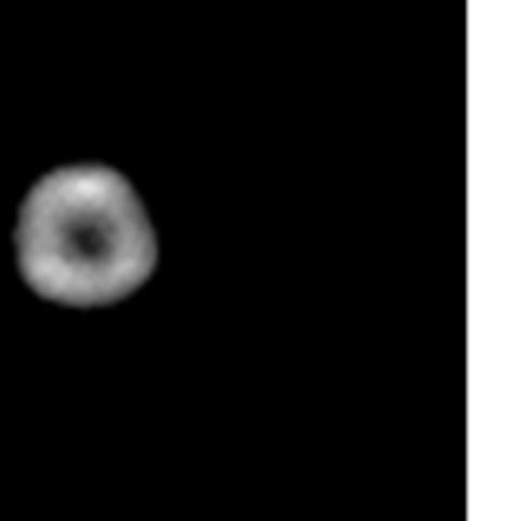
2 2. EXPERIMENTS 2.1 Experimental method Gold films with 5 nm thickness were deposited on glass cover slips with a 2 nm Cr wetting layer by thermal evaporation using an Edward FL 4 thermal evaporator. In the last deposition step, a thin aluminum film was deposited on top of the gold films without breaking the vacuum (base pressure < 1-5 mbar). The aluminum film becomes oxidized entirely upon exposure to ambient environment and turns into an Al 2 O 3 coating. The Al 2 O 3 film thickness was characterized using a Woollam M2 Variable Angle Spectroscopic Ellipsometer. The deposition process was repeated for different gold substrates with similar thickness, while changing the aluminum film thickness. The Al 2 O 3 coatings on four gold substrates were found to have a thickness of 1.3 nm, 1.5 nm, 2.2 nm, and 3.4 nm, respectively. Gold nanoparticle colloidal solution (BBInternational) diluted with ethanol to a concentration of particles/ml with a mean particle diameter of 6.4 ± 2.6 nm was drop coated and left to dry on the Al 2 O 3 coated gold substrates. Darkfield microscopy of nanoparticles on the samples was carried out using an Olympus IX71 inverted microscope equipped with a 5 dark-field objective (UMPlanFL 5 BD, N.A.=.75) and standard dark-field optics. The darkfield images were recorded with two imaging CCD cameras; a Canon EOS 45D digital camera and a HSi-44C Hyperspectral Imaging System (Gooch & Housego). Single particle spectroscopy was conducted in the same set up but sending the scattering signal to a spectrometer (Horiba Jobin-Yvon ihr32 monochromator with Synapse CCD array). The scattering signals of individual particles were obtained from a ~8 8 μm 2 collection area. In order to obtain a single particle scattering spectrum I sc (λ), the collected signal from a particle I NP (λ) was measured, the collected signal from a nearby reference collection area I REF (λ) was subtracted, and the resulting background corrected signal was divided by the collected lamp spectrum I IN (λ), corresponding to the formula I sc =(I NP I REF )/I IN. Approximately one hundred single particle spectra were recorded from the Al 2 O 3 coated gold substrates, including a reference gold substrate without Al 2 O 3 coating. 2.2 Experimental Observation Figure 1(a, solid lines) shows scattering spectra of single gold nanoparticles on different Al 2 O 3 coated gold substrates. The scattering spectra were selected from typical spectra measured in the experiment. The spectra show a clear blueshift upon increasing the Al 2 O 3 coating thickness from to 3.4 nm, with the main scattering peak shifting from 69 nm to 61 nm. In addition to the main scattering peak, there is a weak resonance peak ~55 nm present in all scattering spectra. Figure 1 (b) and (c) show two columns of dark-field microscopy images of the same gold nanoparticle from each substrate recorded with a Canon EOS 45D digital camera and a HSi-44C Hyperspectral Imaging System, respectively. To construct the images in Fig. 1(c), the HSi-44C recorded a set of spectral images of each nanoparticle then the spectral images were combined into a single false-color image. The color bar represents the false-color function as a function of wavelength The processed images help distinguish nanoparticles scattering responses that have similar resonance wavelengths (down to 5 nm spectral resolution) that could not be distinguished using a conventional RGBcamera. Note that the images in Fig. 1(c) show dumbbell-shaped scattering patterns instead of the ring-shaped scattering patterns shown in Figure 1(b). This is the result of the known polarization dependent response of the HSi- 44C. Figure 1(b) and (c) show ring/dumbbell-shaped scattering patterns of single nanoparticles on different substrates. Among these images only Figures 1(b-i) present a clear central scattering signal at green wavelengths (real color image), while its corresponding scattering spectrum suggests the presence of strong scattering at red/nir wavelengths. This is the result of a drop in transmission of IR cut filters in the Canon camera (T <.1 for wavelength longer than 68 nm). The observations in Fig. 1 indicate the co-existences of two resonance modes, lateral and vertical dipole modes. The origin of these two modes will be discussed in the following section. Proc. of SPIE Vol S-2
 Ú W 1 /\ - -, 555 ''-'-'''--r--::_11---/")


 and a HSi-44C Hyperspectral")


 in the simulations.")
3 a) Scatterin spectrum (b) (c) 1 - nm AIrO. - Canon FISi-44C ' I vi) Ú W 1 /\ - -, 555 ''-'-'''--r--::_11---/ V) 1-3A(4) nm AIz3, - OOO nr) i 55 Eì 65 -r' 75 f VI /avelength (irim) Figure 1. Measured (solid) and calculated (dashed) scattering spectra of a gold nanoparticle on Al 2 O 3 coated gold substrates with different Al 2 O 3 thicknesses (a). The thicknesses used in the simulation are listed in parentheses. Five pairs of darkfield images of single nanoparticles on different substrates taken with a Canonn EOS 45D (b) and a HSi-44C Hyperspectral Imaging System (c). The color bar represents the wavelength color scale used to construct the spectral images in (c) NUMERICAL SIMULATION 3.1 Simulation Model and Calculation Method Electromagnetic simulation of the structure used in the experiment was performed using CST Microwave Studio. 9 Figure 2 presents the simulated structure consisting of a 6 nm diameter goldd nanoparticle placed on an Al 2 O 3 coated gold film, with a gold thickness of 5 nm and varying Al 2 O 3 thickness to capture the trends observed in the experiments. Material data of gold and Al 2 O 3 were taken from Ref. 1 and 11, respectively. To take into account the presence of organic ligands on the gold nanoparticles after deposition from colloidal solution, the gold nanoparticle was coated with a 1 nm thick organic shell of (n = 1.5) in the simulations. A 2 nm unit cell boundary was used in the simulations to avoid reflections from any substrate edges. This gives reliablee results as longg as particle-particle interactions are minimal in the simulation. The particle is excited with a plane wave arriving at 77 to the substrate surface normal. The incident angle was chosen to be the same as the darkfield illumination angle usedd in the experiment. Both TE and TM excitation conditions were simulated. Proc. of SPIE Vol S-3
.")
 and the effectivee dipole moment of the gold film (μμ Au ) directly")


")
 (dashed lines) ), the calculated scattering spectra of the gold nanoparticle on an Al 2 O 3 gold film with different Al 2")


, the magnitude of the effective dipole moments of both the nanoparticle (solid lines) and the gold film (dashed lines) are")


 compared to that of")
4 A123 film Figure 2. The schematic of the simulated structure used in the simulationn (a). The tetrahedral meshes of the simulation structure with the unit cell boundary used in the software (b). The scattering spectra were calculated based on the simulated field distributions using a simple integrated dipole scattering assumption. First, the effective dipole moment of the nanoparticle (μ NP ) and the effectivee dipole moment of the gold film (μμ Au ) directly underneath the particle were obtained separately by a volume integration of the particle and substrate polarization (P). The substrate polarization was considered underneath thee nanoparticle within a square area as shown by the fine mesh near the particle in Fig. 2(b). The effective dipole moment of the gold film in this same area but in the absence of a particle was subtracted from the data to avoid taking into account substrate response contributions that produce specular reflection as opposed to scattering. The scattering spectrum was then calculated using the total effective dipole moment of the particle-on-film system (μ total = μ NP + μ Au ) giving the scattering power that is proportional to μ total 2 ω In Figure 1(a) (dashed lines) ), the calculated scattering spectra of the gold nanoparticle on an Al 2 O 3 gold film with different Al 2 O 3 thickness were plotted, showing a similar tuning response as a function of Al 2 O 3 thickness as observed in experiments. 4. RESULTSS AND DISCUSSION As previously mentioned the observed resonance modes and their spectral response will be explained by comparing with the simulation results. Figure 3 presents the effective dipole momentt magnitude and phase of the nanoparticle and the underlying gold film from the simulation with 1.5 nm Al 2 O 3 thickness. Two components are shown, the lateral dipole moment under TE plane wave excitation and the vertical dipole moment under TM plane wave excitation. In Figure 3(a), the magnitude of the effective dipole moments of both the nanoparticle (solid lines) and the gold film (dashed lines) are seen to have a strong vertical dipole moment (red) and a weaker lateral dipole moment (blue). The ratio between the maximum value of the nanoparticle dipole moment magnitudee and the gold film dipole moment magnitude of the lateral and the vertical modes are 3.37 and 2.38, respectively. If f ones consider only the nanoparticle dipole moment without taking into account the substrate contribution, the calculated scattering signal shows noticeable differences compared to the features found in the experiment. Thee main difference is that the calculated scattering spectrum has a stronger peak as the short wavelength (~55 nm) compared to that of the measured spectrum. The differences between the simple scattering spectrum calculation and thee experimentall results are reduced when taking into considerationn the effectivee dipole moment of the gold film underneath the particle. Figure 3(b) reveals the phase relationship between the two effective dipole moments (that of thee particle and the substrate) of the two resonance modes. The plot indicates a clear difference between the lateral and the vertical resonance modes. The lateral dipoles of the nanoparticle and the gold film are seen to be out of phase acrosss the entire wavelength range of interest while the vertical dipole moments stay in-phase. These factors result in a strongg vertical scattering component at long wavelength and a reduced lateral scattering component of the gold nanoparticle on Al 2 O 3 coated gold films, as also observed in the measure spectra. Proc. of SPIE Vol S-4
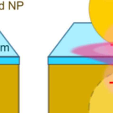
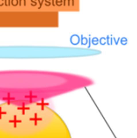
5 i - Lateral NP dipole - Vertical NP dipole - Lateral Au film dipole - Vertical Au film dipole (a) r (b)_ Wavelength (nim) Figure 3. The effective lateral and vertical dipole moment magnitude (a) and phase (b) off the gold nanoparticle and the gold film upon excitation with TE and TM waves, respectively. Figure 4 presents the dark field scattering images of a gold nanoparticle on an All 2 O 3 coated gold film with a 1.5 nm Al 2 O 3 thickness (same as Figure 1 row ii) ). The top row shows a schematic drawing of how scattering associated with the lateral and the vertical resonance modes are collected by the objective lens and thee CCD cameras. Image dipoles in the gold substrate are drawn schematically with the respective phases to the nanoparticle dipoles as found in the numerical simulation results shown in Figure 3. The middle and the bottom rows show the combined and separated images corresponding to the two scattering image modes of the same particlee recorded with a Canon EOS 45D digital camera and a HSi-44C Hyperspectral Imaging System, respectively. The decomposed images were converted to gray-scale to facilitate a comparison between the scattering patterns of the two modes. The right column represents the scattering of the stronger peak of the scattering spectrum which is seen to show a clear evidence of the vertical dipole modes (ring/dumbbell shaped). The weak lateral dipole mode was enhanced (the Red signal of the RGB camera was removed/only a spectral image at 55 nm from the Hyperspectral camera was selected, the brightness and contrast were adjusted) to highlight the difference in scattering pattern for the resonance modes in this particle-on-film plasmonic system. The short-wavelength scattering pattern shows a central scattering spot similar to the observation in Figure 1(b) row i, wheree the long wavelength response was cut by the Canonn camera transmission window. The experimental observations closely match the expectations based on the simulated dipole momentss of the nanoparticle and the induced dynamic image charge in the substrate, providing a clear explanation of the development of the distinct scattering patterns commonly observed in single particle spectroscopy studies off particle-on-film structures. Proc. of SPIE Vol S-5
 Blue + Gr chann 223 1 Is")

 of the coupling between")


 and the")


.")


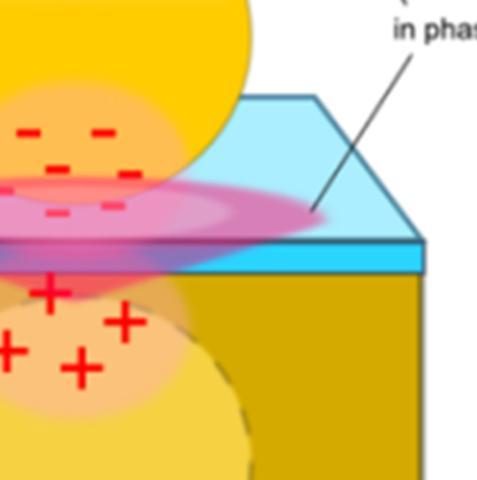
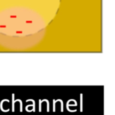
6 (a) Latea (b) Total (c) VE rtical NP i) Blue + Gr chann Is Red channel ii) -.. I.,S dnm Figure 4. Row i) Schematic representations (top row) of the coupling between the gold nanoparticle and the gold film in the presence of a 1.5 nm thick Al 2 O 3 spacer layer due to the formation of dynamic image charges, showing separately the lateral (left column) and the vertical (right column) charge motion and corresponding scatteringg patterns collected by the digital RGB camera (second row) and the spectral imaging system (third row). The central column represents the composite data under dark-field illumination resulting in the simultaneous excitation of both lateral and vertical dipole moment. 5. CONCLUSION Plasmon resonance modes of a gold nanoparticle on an Al 2 O 3 coated gold film are investigated as a model for the interactions occurring in particle-on-film plasmonic structures. Thee scattering spectra of gold nanoparticles show a blueshift of the scattering signal originating from a vertical dipole moment from 69 nm to 61 nm as the Al 2 2O 3 layer thickness increases from to 3.4 nm. The scattering peak associated with a lateral oscillatory dipole moment stays independent of the Al 2 O 3 thickness at ~ 55 nm. The characteristic of the two resonance modes emerges from the difference in coupling between the effective dipole moments of the nanoparticle and the gold film when the particle is excited by light with different polarization directions. Numerical simulations show that the laterall dipole moment of the nanoparticle and the gold film have a ~18 phase difference, causingg a weak net dipole and weak scattering in the short wavelength region. The vertical dipoles on the other hand are almost perfectly in phase, resulting in a strong plasmon resonant scattering signal in the long wavelength region. Decomposed darkfield images visually demonstratee the cothe existence of the two resonance modes and their scattering patterns,, and how thee scattering is projected to CCD Proc. of SPIE Vol S-6
7 cameras. The study explicitly demonstrates the origin of the characteristic particle appearance in scattering images and relative peak strength in scattering spectra of metal-particle-on-film structures. In addition, the method is based on a simple dipole integration technique facilitated by numerical simulation software which is easy to implement. REFERENCES [1] Halas, N. J., Lal, S., Chang, W. S., Link, S. and Nordlander, P., "Plasmons in Strongly Coupled Metallic Nanostructures," Chem Rev 111(6), (211). [2] Mokkapati, S., Beck, F. J., de Waele, R., Polman, A. and Catchpole, K. R., "Resonant nano-antennas for light trapping in plasmonic solar cells," J Phys D Appl Phys 44(18), (211). [3] Mubeen, S., Zhang, S. P., Kim, N., Lee, S., Kramer, S., Xu, H. X. and Moskovits, M., "Plasmonic Properties of Gold Nanoparticles Separated from a Gold Mirror by an Ultrathin Oxide," Nano Lett 12(4), (212). [4] Li, L., Hutter, T., Steiner, U. and Mahajan, S., "Single molecule SERS and detection of biomolecules with a single gold nanoparticle on a mirror junction," The Analyst 138(16), (213). [5] Knight, M. W., Wu, Y. P., Lassiter, J. B., Nordlander, P. and Halas, N. J., "Substrates Matter: Influence of an Adjacent Dielectric on an Individual Plasmonic Nanoparticle," Nano Lett 9(5), (29). [6] Mock, J. J., Hill, R. T., Degiron, A., Zauscher, S., Chilkoti, A. and Smith, D. R., "Distance-Dependent Plasmon Resonant Coupling between a Gold Nanoparticle and Gold Film," Nano Lett 8(8), (28). [7] Hutter, T., Elliott, S. R. and Mahajan, S., "Interaction of metallic nanoparticles with dielectric substrates: effect of optical constants," Nanotechnology 24(3), (213). [8] Nordlander, P. and Prodan, E., "Plasmon hybridization in nanoparticles near metallic surfaces," Nano Lett 4(11), (24). [9] CST MICROWAVE STUDIO, Computer Simulation Technology, Darmstadt, Germany, (212). [1] Johnson, P. B. and Christy, R. W., "Optical Constants of the Noble Metals," Phys Rev B 6(12), (1972). [11] Palik, E. D. and Ghosh, G., [Handbook of Optical Constants of Solids], Academic Press, Orlando; London, (1985). [12] Jackson, J. D., [Classical Electrodynamics], Wiley, New York, (1962). Proc. of SPIE Vol S-7
Invited Paper ABSTRACT 1. INTRODUCTION
 Invited Paper Numerical Prediction of the Effect of Nanoscale Surface Roughness on Film-coupled Nanoparticle Plasmon Resonances Chatdanai Lumdee and Pieter G. Kik *,, CREOL, the College of Optics and Photonics;
ABSTRACT 1. INTRODUCTION
 Cascaded plasmon resonances multi-material nanoparticle trimers for extreme field enhancement S. Toroghi a, Chatdanai Lumdee a, and P. G. Kik* a CREOL, The College of Optics and Photonics, University of
Voltage Controlled Nanoparticle Plasmon Resonance Tuning through Anodization Chatdanai Lumdee a and Pieter G. Kik *,a,b
 Voltage Controlled Nanoparticle Plasmon Resonance Tuning through Anodization Chatdanai Lumdee a and Pieter G. Kik *,a,b a CREOL, the College of Optics and Photonics; b Physics Department, University of
Taking cascaded plasmonic field enhancement to the ultimate limit in silver nanoparticle dimers S. Toroghi* a, P. G. Kik a,b
 Taking cascaded plasmonic field enhancement to the ultimate limit in silver nanoparticle dimers S. Toroghi* a, P. G. Kik a,b a CREOL, The College of Optics and Photonics, University of Central Florida,
Collective effects in second-harmonic generation from plasmonic oligomers
 Supporting Information Collective effects in second-harmonic generation from plasmonic oligomers Godofredo Bautista,, *, Christoph Dreser,,, Xiaorun Zang, Dieter P. Kern,, Martti Kauranen, and Monika Fleischer,,*
Supplementary Information
 Electronic Supplementary Material (ESI) for Nanoscale. This journal is The Royal Society of Chemistry 2014 Supplementary Information Large-scale lithography-free metasurface with spectrally tunable super
Supporting Information:
 Supporting Information: Achieving Strong Field Enhancement and Light Absorption Simultaneously with Plasmonic Nanoantennas Exploiting Film-Coupled Triangular Nanodisks Yang Li, Dezhao Li, Cheng Chi, and
Supporting Information. Plasmon Ruler for Measuring Dielectric Thin Films
 Supporting Information Single Nanoparticle Based Hetero-Nanojunction as a Plasmon Ruler for Measuring Dielectric Thin Films Li Li, *a,b Tanya Hutter, c Wenwu Li d and Sumeet Mahajan *b a School of Chemistry
SUPPLEMENTARY INFORMATION
 SUPPLEMENTARY INFORMATION doi: 10.1038/nnano.2011.72 Tunable Subradiant Lattice Plasmons by Out-of-plane Dipolar Interactions Wei Zhou and Teri W. Odom Optical measurements. The gold nanoparticle arrays
Biosensing based on slow plasmon nanocavities
 iosensing based on slow plasmon nanocavities. Sepulveda, 1, Y. Alaverdyan,. rian, M. Käll 1 Nanobiosensors and Molecular Nanobiophysics Group Research Center on Nanoscience and Nanotechnolog (CIN)CSIC-ICN
Full-color Subwavelength Printing with Gapplasmonic
 Supporting information for Full-color Subwavelength Printing with Gapplasmonic Optical Antennas Masashi Miyata, Hideaki Hatada, and Junichi Takahara *,, Graduate School of Engineering, Osaka University,
U-Shaped Nano-Apertures for Enhanced Optical Transmission and Resolution
 U-Shaped Nano-Apertures for Enhanced Optical Transmission and Resolution Mustafa Turkmen 1,2,3, Serap Aksu 3,4, A. Engin Çetin 2,3, Ahmet A. Yanik 2,3, Alp Artar 2,3, Hatice Altug 2,3,4, * 1 Electrical
Strong plasmon coupling between two gold nanospheres on a gold slab
 Strong plasmon coupling between two gold nanospheres on a gold slab H. Liu 1, *, J. Ng 2, S. B. Wang 2, Z. H. Hang 2, C. T. Chan 2 and S. N. Zhu 1 1 National Laboratory of Solid State Microstructures and
Nano Optics Based on Coupled Metal Nanoparticles
 Nano Optics Based on Coupled Metal Nanoparticles Shangjr Gwo ( 果尚志 ) Department of Physics National Tsing-Hua University, Hsinchu 30013, Taiwan E-mail: gwo@phys.nthu.edu.tw NDHU-Phys (2010/03/01) Background
Supporting Information. Single-Particle Absorption Spectroscopy by. Photothermal Contrast
 Supporting Information Single-Particle Absorption Spectroscopy by Photothermal Contrast Mustafa Yorulmaz 1,, Sara Nizzero 2, 3,, Anneli Hoggard 1, Lin-Yung Wang 1, Yi-Yu Cai 1, Man-Nung Su 1, Wei-Shun
Supplementary Information Effects of asymmetric nanostructures on the extinction. difference properties of actin biomolecules and filaments
 Supplementary Information Effects of asymmetric nanostructures on the extinction difference properties of actin biomolecules and filaments 1 E. H. Khoo, 2 Eunice S. P. Leong, 1 W. K. Phua, 2 S. J. Wu,
Nanoscale Control of Gap-plasmon Enhanced Optical Processes
 University of Central Florida Electronic Theses and Dissertations Doctoral Dissertation (Open Access) Nanoscale Control of Gap-plasmon Enhanced Optical Processes 2015 Chatdanai Lumdee University of Central
Simulated Study of Plasmonic Coupling in Noble Bimetallic Alloy Nanosphere Arrays
 CHAPTER 4 Simulated Study of Plasmonic Coupling in Noble Bimetallic Alloy Nanosphere Arrays 4.1 Introduction In Chapter 3, the noble bimetallic alloy nanosphere (BANS) of Ag 1-x Cu x at a particular composition
Supplementary Figure S1 Anticrossing and mode exchange between D1 (Wood's anomaly)
") Supplementary Figure S1 Anticrossing and mode exchange between D1 (Wood's anomaly) and D3 (Fabry Pérot cavity mode). (a) Schematic (top) showing the reflectance measurement geometry and simulated angle-resolved
Supplementary Figure S1 Anticrossing and mode exchange between D1 (Wood's anomaly) and D3 (Fabry Pérot cavity mode). (a) Schematic (top) showing the reflectance measurement geometry and simulated angle-resolved
Three-dimensional Visualization and Quantification of Gold Nanomaterial Deposition and Aggregation in Porous Media via Raman Spectroscopy
 Raman Spectroscopy Nanomaterials Exposure? Three-dimensional Visualization and Quantification of Gold Nanomaterial Deposition and Aggregation in Porous Media via Raman Spectroscopy Matthew Y. Chan, Weinan
ECE280: Nano-Plasmonics and Its Applications. Week8
 ECE280: Nano-Plasmonics and Its Applications Week8 Surface Enhanced Raman Scattering (SERS) and Surface Plasmon Amplification by Stimulated Emission of Radiation (SPASER) Raman Scattering Chandrasekhara
Near-field imaging and spectroscopy of electronic states in single-walled carbon nanotubes
 Early View publication on www.interscience.wiley.com (issue and page numbers not yet assigned; citable using Digital Object Identifier DOI) Original phys. stat. sol. (b), 1 5 (2006) / DOI 10.1002/pssb.200669179
Natallia Strekal. Plasmonic films of noble metals for nanophotonics
 Natallia Strekal Plasmonic films of noble metals for nanophotonics The aim of our investigation is the mechanisms of light interactions with nanostructure and High Tech application in the field of nanophotonics
Embedded metallic nanopatterns for enhanced optical absorption
 Embedded metallic nanopatterns for enhanced optical absorption Fan Ye, Michael J. Burns, Michael J. Naughton* Department of Physics, Boston College, Chestnut Hill MA 02467 ABSTRACT Novel metallic nanopatterns
Optical properties of spherical and anisotropic gold shell colloids
 8 Optical properties of spherical and anisotropic gold shell colloids Core/shell colloids consisting of a metal shell and a dielectric core are known for their special optical properties. The surface plasmon
Heterodimer nanostructures induced energy focusing on metal
 Heterodimer nanostructures induced energy focusing on metal film Ting Liu a, Jingjing Hao a, Yingzhou Huang*,a, Xun Su a, Li Hu a and Yurui Fang*,b a Soft Matter and Interdisciplinary Research Center,
Nanosphere Lithography
 Nanosphere Lithography Derec Ciafre 1, Lingyun Miao 2, and Keita Oka 1 1 Institute of Optics / 2 ECE Dept. University of Rochester Abstract Nanosphere Lithography is quickly emerging as an efficient, low
Study of Surface Plasmon Excitation on Different Structures of Gold and Silver
 Nanoscience and Nanotechnology 2015, 5(4): 71-81 DOI: 10.5923/j.nn.20150504.01 Study of Surface Plasmon Excitation on Different Structures of Gold and Silver Anchu Ashok 1,*, Arya Arackal 1, George Jacob
Visualizing the bi-directional electron transfer in a Schottky junction consisted of single CdS nanoparticles and a planar gold film
 Electronic Supplementary Material (ESI) for Chemical Science. This journal is The Royal Society of Chemistry 2017 Electronic Supplementary Information Visualizing the bi-directional electron transfer in
Nanoscale optical circuits: controlling light using localized surface plasmon resonances
 Nanoscale optical circuits: controlling light using localized surface plasmon resonances T. J. Davis, D. E. Gómez and K. C. Vernon CSIRO Materials Science and Engineering Localized surface plasmon (LSP)
Single Emitter Detection with Fluorescence and Extinction Spectroscopy
 Single Emitter Detection with Fluorescence and Extinction Spectroscopy Michael Krall Elements of Nanophotonics Associated Seminar Recent Progress in Nanooptics & Photonics May 07, 2009 Outline Single molecule
HYPER-RAYLEIGH SCATTERING AND SURFACE-ENHANCED RAMAN SCATTERING STUDIES OF PLATINUM NANOPARTICLE SUSPENSIONS
 www.arpapress.com/volumes/vol19issue1/ijrras_19_1_06.pdf HYPER-RAYLEIGH SCATTERING AND SURFACE-ENHANCED RAMAN SCATTERING STUDIES OF PLATINUM NANOPARTICLE SUSPENSIONS M. Eslamifar Physics Department, BehbahanKhatamAl-Anbia
The effects of probe boundary conditions and propagation on nano- Raman spectroscopy
 The effects of probe boundary conditions and propagation on nano- Raman spectroscopy H. D. Hallen,* E. J. Ayars** and C. L. Jahncke*** * Physics Department, North Carolina State University, Raleigh, NC
Supporting Information
 Copyright WILEY VCH Verlag GmbH & Co. KGaA,69469 Weinheim,Germany,2011 Supporting Information for Small,DOI: 10.1002/ smll.201100371 Lithographically Fabricated Optical Antennas with Gaps Well Below 10
Supplementary Note 1: Dark field measurements and Scattering properties of NPoM geometries
 Supplementary Note 1: Dark field measurements and Scattering properties of NPoM geometries Supplementary Figure 1: Dark field scattering properties of individual nanoparticle on mirror geometries separated
Supplementary Figure S1 SEM and optical images of Si 0.6 H 0.4 colloids. a, SEM image of Si 0.6 H 0.4 colloids. b, The size distribution of Si 0.
 Supplementary Figure S1 SEM and optical images of Si 0.6 H 0.4 colloids. a, SEM image of Si 0.6 H 0.4 colloids. b, The size distribution of Si 0.6 H 0.4 colloids. The standard derivation is 4.4 %. Supplementary
Prediction and Optimization of Surface-Enhanced Raman Scattering Geometries using COMSOL Multiphysics
 Excerpt from the Proceedings of the COMSOL Conference 2008 Hannover Prediction and Optimization of Surface-Enhanced Raman Scattering Geometries using COMSOL Multiphysics I. Knorr 1, K. Christou,2, J. Meinertz
Vibrational Spectroscopies. C-874 University of Delaware
 Vibrational Spectroscopies C-874 University of Delaware Vibrational Spectroscopies..everything that living things do can be understood in terms of the jigglings and wigglings of atoms.. R. P. Feymann Vibrational
SUPPLEMENTARY INFORMATION
 SUPPLEMENTARY INFORMATION Nano-scale plasmonic motors driven by light Ming Liu 1, Thomas Zentgraf 1, Yongmin Liu 1, Guy Bartal 1 & Xiang Zhang 1,2 1 NSF Nano-scale Science and Engineering Center (NSEC),
[Electronic Supplementary Information]
![[Electronic Supplementary Information]](/thumbs/95/123080639.jpg "[Electronic Supplementary Information]") [Electronic Supplementary Information] Tuning the Interparticle Distance in Nanoparticle Assemblies in Suspension via DNA-Triplex Formation: Correlation Between Plasmonic and Surface-enhanced Raman Scattering
[Electronic Supplementary Information] Tuning the Interparticle Distance in Nanoparticle Assemblies in Suspension via DNA-Triplex Formation: Correlation Between Plasmonic and Surface-enhanced Raman Scattering
Methods. Single nanoparticle spectroscopy
 Methods Supplementary Figure 1. Substrate used to localize and characterize individual plasmonic structures. (a) A photo showing the quartz substrate, which is divided into periods of 5 5 units as depicted
Light trapping in thin-film solar cells: the role of guided modes
 Light trapping in thin-film solar cells: the role of guided modes T. Søndergaard *, Y.-C. Tsao, T. G. Pedersen, and K. Pedersen Department of Physics and Nanotechnology, Aalborg University, Skjernvej 4A,
Scattering cross-section (µm 2 )
") Supplementary Figures Scattering cross-section (µm 2 ).16.14.12.1.8.6.4.2 Total scattering Electric dipole, a E (1,1) Magnetic dipole, a M (1,1) Magnetic quardupole, a M (2,1). 44 48 52 56 Wavelength (nm)
Supplementary Figures Scattering cross-section (µm 2 ).16.14.12.1.8.6.4.2 Total scattering Electric dipole, a E (1,1) Magnetic dipole, a M (1,1) Magnetic quardupole, a M (2,1). 44 48 52 56 Wavelength (nm)
Optical properties of TiO2:Ag composites
 Optical properties of TiO:Ag composites Krzysztof Skorupski a a Wroclaw University of Technology, Chair of Electronics and Photonics Metrology, Boleslawa Prusa 53/55, 50-31 Wroclaw, Poland ABSTRACT The
Diversifying Nanoparticle Assemblies in. Supramolecule Nanocomposites Via Cylindrical
 Diversifying Nanoparticle Assemblies in Supramolecule Nanocomposites Via Cylindrical Confinement Peter Bai, Sui Yang, Wei Bao ǁ, Joseph Kao, Kari Thorkelsson, Miquel Salmeron ǁ, Xiang Zhang ǁ, Ting Xu
Supplementary Information
 Electronic Supplementary Material (ESI) for Nanoscale. This journal is The Royal Society of Chemistry 2017 Supplementary Information Coupling Effects in 3D Plasmonic Structures Templated by Morpho Butterfly
Simulation of Surface Plasmon Resonance on Different Size of a Single Gold Nanoparticle
 Journal of Physics: Conference Series PAPER OPEN ACCESS Simulation of Surface Plasmon Resonance on Different Size of a Single Gold Nanoparticle To cite this article: Norsyahidah Md Saleh and A. Abdul Aziz
"Surface-Enhanced Raman Scattering
 SMR: 1643/11 WINTER COLLEGE ON OPTICS ON OPTICS AND PHOTONICS IN NANOSCIENCE AND NANOTECHNOLOGY ( 7-18 February 2005) "Surface-Enhanced Raman Scattering presented by: Martin Moskovits University of California,
arxiv: v1 [cond-mat.mes-hall] 16 Nov 2011
![arxiv: v1 [cond-mat.mes-hall] 16 Nov 2011](/thumbs/89/98895994.jpg "arxiv: v1 [cond-mat.mes-hall] 16 Nov 2011") EXPLORING THE PARAMETER SPACE OF DISC SHAPED SILVER NANOPARTICLES FOR THIN FILM SILICON PHOTOVOLTAICS arxiv:.379v [cond-mat.mes-hall] 6 Nov 2 BRUNO FIGEYS, OUNSI EL DAIF IMEC VZW, LEUVEN, BELGIUM Abstract.
EXPLORING THE PARAMETER SPACE OF DISC SHAPED SILVER NANOPARTICLES FOR THIN FILM SILICON PHOTOVOLTAICS arxiv:.379v [cond-mat.mes-hall] 6 Nov 2 BRUNO FIGEYS, OUNSI EL DAIF IMEC VZW, LEUVEN, BELGIUM Abstract.
Multiple Fano Resonances Structure for Terahertz Applications
 Progress In Electromagnetics Research Letters, Vol. 50, 1 6, 2014 Multiple Fano Resonances Structure for Terahertz Applications Hadi Amarloo *, Daniel M. Hailu, and Safieddin Safavi-Naeini Abstract A new
Aluminum for nonlinear plasmonics: Methods Section
 Aluminum for nonlinear plasmonics: Methods Section Marta Castro-Lopez, Daan Brinks, Riccardo Sapienza, and Niek F. van Hulst, ICFO - Institut de Ciencies Fotoniques, and ICREA - Institució Catalana de
Supporting information for the communication Label-Free Aptasensor. Based on Ultrathin-Linker-Mediated Hot-Spot Assembly to Induce
 Supporting information for the communication Label-Free Aptasensor Based on Ultrathin-Linker-Mediated Hot-Spot Assembly to Induce Strong Directional Fluorescence. Shuo-Hui Cao 1, Wei-Peng Cai 1, Qian Liu
Advanced Spectroscopy Laboratory
 Advanced Spectroscopy Laboratory - Raman Spectroscopy - Emission Spectroscopy - Absorption Spectroscopy - Raman Microscopy - Hyperspectral Imaging Spectroscopy FERGIELAB TM Raman Spectroscopy Absorption
Single Particle Spectroscopy Study of Metal-Film-Induced Tuning of Silver Nanoparticle Plasmon Resonances
 J. Phys. Chem. C 2010, 114, 7509 7514 7509 Single Particle Spectroscopy Study of Metal-Film-Induced Tuning of Silver Nanoparticle Plasmon Resonances Min Hu,, Amitabh Ghoshal, Manuel Marquez, and Pieter
SUPPLEMENTARY INFORMATION
 SUPPLEMENTARY INFORMATION Coupling of Plasmonic Nanopore Pairs: Facing Dipoles Attract Each Other Takumi Sannomiya 1, Hikaru Saito 2, Juliane Junesch 3, Naoki Yamamoto 1. 1 Department of Innovative and
Evaluating nanogaps in Ag and Au nanoparticle clusters for SERS applications using COMSOL Multiphysics
 Evaluating nanogaps in Ag and Au nanoparticle clusters for SERS applications using COMSOL Multiphysics Ramesh Asapu 1, Radu-George Ciocarlan 2, Nathalie Claes 3, Natan Blommaerts 1, Sara Bals 3, Pegie
Plasmonic Photovoltaics Harry A. Atwater California Institute of Technology
 Plasmonic Photovoltaics Harry A. Atwater California Institute of Technology Surface plasmon polaritons and localized surface plasmons Plasmon propagation and absorption at metal-semiconductor interfaces
Flexible, Transparent and Highly Sensitive SERS. Substrates with Cross-nanoporous Structures for
 Electronic Supplementary Material (ESI) for Nanoscale. This journal is The Royal Society of Chemistry 2018 supplementary information Flexible, Transparent and Highly Sensitive SERS Substrates with Cross-nanoporous
Efficient Hydrogen Evolution. University of Central Florida, 4000 Central Florida Blvd. Orlando, Florida, 32816,
 Electronic Supplementary Material (ESI) for Energy & Environmental Science. This journal is The Royal Society of Chemistry 2017 MoS 2 /TiO 2 Heterostructures as Nonmetal Plasmonic Photocatalysts for Highly
JOURNAL OF APPLIED PHYSICS 101,
 JOURNAL OF APPLIED PHYSICS 101, 104309 2007 Photocurrent spectroscopy of optical absorption enhancement in silicon photodiodes via scattering from surface plasmon polaritons in gold nanoparticles S. H.
Printing Colour at the Optical Diffraction Limit
 SUPPLEMENTARY INFORMATION DOI: 10.1038/NNANO.2012.128 Printing Colour at the Optical Diffraction Limit Karthik Kumar 1,#, Huigao Duan 1,#, Ravi S. Hegde 2, Samuel C.W. Koh 1, Jennifer N. Wei 1 and Joel
Plasmonic properties and sizing of core-shell Cu-Cu 2 O nanoparticles fabricated by femtosecond laser ablation in liquids ABSTRACT
 Plasmonic properties and sizing of core-shell Cu-Cu O nanoparticles fabricated by femtosecond laser ablation in liquids J. M. J. Santillán 1, F. A. Videla 1,, D. C. Schinca 1, and L. B. Scaffardi 1, 1
Optical cavity modes in gold shell particles
 9 Optical cavity modes in gold shell particles Gold (Au) shell particles with dimensions comparable to the wavelength of light exhibit a special resonance, with a tenfold field enhancement over almost
Plasmonics. The long wavelength of light ( μm) creates a problem for extending optoelectronics into the nanometer regime.
 creates a problem for extending optoelectronics into the nanometer regime.") Plasmonics The long wavelength of light ( μm) creates a problem for extending optoelectronics into the nanometer regime. A possible way out is the conversion of light into plasmons. They have much shorter
Plasmonics The long wavelength of light ( μm) creates a problem for extending optoelectronics into the nanometer regime. A possible way out is the conversion of light into plasmons. They have much shorter
Supplementary information for. plasmonic nanorods interacting with J-aggregates.
 Supplementary information for Approaching the strong coupling limit in single plasmonic nanorods interacting with J-aggregates. by Gülis Zengin, Göran Johansson, Peter Johansson, Tomasz J. Antosiewicz,
Spatial Coherence Properties of Organic Molecules Coupled to Plasmonic Surface Lattice Resonances in the Weak and Strong Coupling Regimes
 Spatial Coherence Properties of Organic Molecules Coupled to Plasmonic Surface Lattice Resonances in the Weak and Strong Coupling Regimes Supplemental Material L. Shi, T. K. Hakala, H. T. Rekola, J. -P.
Supporting Information
 Supporting Information Highly Sensitive, Reproducible, and Stable SERS Sensors Based on Well-Controlled Silver Nanoparticles Decorated Silicon Nanowire Building Blocks Xue Mei Han, Hui Wang, Xue Mei Ou,
Electronic Supplementary Information. Au/Ag Core-shell Nanocuboids for High-efficiency Organic Solar Cells with Broadband Plasmonic Enhancement
 Electronic Supplementary Material (ESI) for Energy & Environmental Science. This journal is The Royal Society of Chemistry 2016 Electronic Supplementary Information Au/Ag Core-shell Nanocuboids for High-efficiency
Controlling Fano lineshapes in plasmon-mediated light coupling into a substrate
 Controlling Fano lineshapes in plasmon-mediated light coupling into a substrate P. Spinelli,* C. van Lare, E. Verhagen, and A. Polman Center for Nanophotonics, FOM Institute AMOLF Science Park, 98 XG,
The Dielectric Function of a Metal ( Jellium )
") The Dielectric Function of a Metal ( Jellium ) Total reflection Plasma frequency p (10 15 Hz range) Why are Metals Shiny? An electric field cannot exist inside a metal, because metal electrons follow the
The Dielectric Function of a Metal ( Jellium ) Total reflection Plasma frequency p (10 15 Hz range) Why are Metals Shiny? An electric field cannot exist inside a metal, because metal electrons follow the
Supporting Information s for
 Supporting Information s for # Self-assembling of DNA-templated Au Nanoparticles into Nanowires and their enhanced SERS and Catalytic Applications Subrata Kundu* and M. Jayachandran Electrochemical Materials
Surface Plasmon Resonance in Metallic Nanoparticles and Nanostructures
 Surface Plasmon Resonance in Metallic Nanoparticles and Nanostructures Zhi-Yuan Li Optical Physics Laboratory, Institute of Physics, CAS Beijing 18, China January 5-9, 7, Fudan University, Shanghai Challenges
Broadband Plasmonic Couplers for Light Trapping and Waveguiding
 Broadband Plasmonic Couplers for Light Trapping and Waveguiding F. Djidjeli* a, E. Jaberansary a, H. M. H. Chong a, and D. M. Bagnall a a Nano Research Group, School of Electronics and Computer Science,
PERIODIC ARRAYS OF METAL NANOBOWLS AS SERS-ACTIVE SUBSTRATES
 PERIODIC ARRAYS OF METAL NANOBOWLS AS SERS-ACTIVE SUBSTRATES Lucie ŠTOLCOVÁ a, Jan PROŠKA a, Filip NOVOTNÝ a, Marek PROCHÁZKA b, Ivan RICHTER a a Czech Technical University in Prague, Faculty of Nuclear
Electronic Supplementary Information
 Electronic Supplementary Material (ESI) for Physical Chemistry Chemical Physics. This journal is the Owner Societies 2014 Electronic Supplementary Information CW-Laser-Induced Morphological Changes of
Plasmon enhancement of optical absorption in ultra-thin film solar cells by rear located aluminum nanodisk arrays
 Opt Quant Electron (2017)49:161 DOI 10.1007/s11082-017-0930-x Plasmon enhancement of optical absorption in ultra-thin film solar cells by rear located aluminum nanodisk arrays Debao Zhang 1 Yawei Kuang
ABSTRACT 1. INTRODUCTION
 Optimization of Surface Plasmon Excitation Using Resonant Nanoparticle Arrays above a Silver Film Amitabh Ghoshal, Pieter G. Kik CREOL: College of Optics and Photonics, University of Central Florida, Central
7. Localized surface plasmons (Particle plasmons)
") 7. Localized surface plasmons (Particle plasmons) ( Plasmons in metal nanostructures, Dissertation, University of Munich by Carsten Sonnichsen, 2001) Lycurgus cup, 4th century (now at the British Museum,
7. Localized surface plasmons (Particle plasmons) ( Plasmons in metal nanostructures, Dissertation, University of Munich by Carsten Sonnichsen, 2001) Lycurgus cup, 4th century (now at the British Museum,
Fundamentals of nanoscience
 Fundamentals of nanoscience Spectroscopy of nano-objects Mika Pettersson 1. Non-spatially resolved spectroscopy Traditionally, in spectroscopy, one is interested in obtaining information on the energy
Gold-black as IR absorber and solar cell enhancer
 Gold-black as IR absorber and solar cell enhancer Journal: 2009 MRS Fall Meeting Manuscript ID: Draft Symposium: Symposium O Date Submitted by the Author: Complete List of Authors: Peale, Robert; University
Polarization-Dependent Surface Enhanced Raman Scattering from Silver 1D Nanoparticle Arrays
 11609 2008, 112, 11609 11613 Published on Web 07/11/2008 Polarization-Dependent Surface Enhanced Raman Scattering from Silver 1D Nanoparticle Arrays Wei Luo,, Wytze van der Veer, Ping Chu, D. L. Mills,
Plasmonic fractals: ultrabroadband light trapping in thin film solar cells by a Sierpinski nanocarpet
 Plasmonic fractals: ultrabroadband light trapping in thin film solar cells by a Sierpinski nanocarpet Hanif Kazerooni 1, Amin Khavasi, 2,* 1. Chemical Engineering Faculty, Amirkabir University of Technology
Negative Index of Refraction in Optical Metamaterials
 1 Negative Index of Refraction in Optical Metamaterials V. M. Shalaev, W. Cai, U. Chettiar, H.-K. Yuan, A. K. Sarychev, V. P. Drachev, and A. V. Kildishev School of Electrical and Computer Engineering,
Localized surface plasmons (Particle plasmons)
") Localized surface plasmons (Particle plasmons) ( Plasmons in metal nanostructures, Dissertation, University of Munich by Carsten Sonnichsen, 2001) Lycurgus cup, 4th century (now at the British Museum,
Localized surface plasmons (Particle plasmons) ( Plasmons in metal nanostructures, Dissertation, University of Munich by Carsten Sonnichsen, 2001) Lycurgus cup, 4th century (now at the British Museum,
Supporting Information to Multiband Plasmonic Sierpinski Carpet Fractal Antennas
 Supporting Information to Multiband Plasmonic Sierpinski Carpet Fractal Antennas Francesco De Nicola, 1, Nikhil Santh Puthiya Purayil, 1, 2 Davide Spirito, 3 Mario Miscuglio, 3, 4 Francesco Tantussi, 5
l* = 109 nm Glycerol Clean Water Glycerol l = 108 nm Wavelength (nm)
") 1/ (rad -1 ) Normalized extinction a Clean 0.8 Water l* = 109 nm 0.6 Glycerol b 2.0 1.5 500 600 700 800 900 Clean Water 0.5 Glycerol l = 108 nm 630 660 690 720 750 Supplementary Figure 1. Refractive index
1/ (rad -1 ) Normalized extinction a Clean 0.8 Water l* = 109 nm 0.6 Glycerol b 2.0 1.5 500 600 700 800 900 Clean Water 0.5 Glycerol l = 108 nm 630 660 690 720 750 Supplementary Figure 1. Refractive index
Enhanced Photonic Properties of Thin Opaline Films as a Consequence of Embedded Nanoparticles.
 Enhanced Photonic Properties of Thin Opaline Films as a Consequence of Embedded Nanoparticles. D E Whitehead, M Bardosova and M E Pemble Tyndall National Institute, University College Cork Ireland Introduction:
Optimizing the performance of metal-semiconductor-metal photodetectors by embedding nanoparticles in the absorption layer
 Journal of Electrical and Electronic Engineering 2015; 3(2-1): 78-82 Published online February 10, 2015 (http://www.sciencepublishinggroup.com/j/jeee) doi: 10.11648/j.jeee.s.2015030201.27 ISSN: 2329-1613
Backscattering enhancement of light by nanoparticles positioned in localized optical intensity peaks
 Backscattering enhancement of light by nanoparticles positioned in localized optical intensity peaks Zhigang Chen, Xu Li, Allen Taflove, and Vadim Backman We report what we believe to be a novel backscattering
Wednesday 3 September Session 3: Metamaterials Theory (16:15 16:45, Huxley LT308)
") Session 3: Metamaterials Theory (16:15 16:45, Huxley LT308) (invited) TBC Session 3: Metamaterials Theory (16:45 17:00, Huxley LT308) Light trapping states in media with longitudinal electric waves D McArthur,
Session 3: Metamaterials Theory (16:15 16:45, Huxley LT308) (invited) TBC Session 3: Metamaterials Theory (16:45 17:00, Huxley LT308) Light trapping states in media with longitudinal electric waves D McArthur,
Mixed Dimer Double-Resonance Substrates for Surface-Enhanced Raman Spectroscopy
 Mixed Dimer Double-Resonance Substrates for Surface-Enhanced Raman Spectroscopy Mohamad G. Banaee* and Kenneth B. Crozier* School of Engineering and Applied Sciences, Harvard University, Cambridge, Massachusetts
Nanoscale Chemical Imaging with Photo-induced Force Microscopy
 OG2 BCP39nm_0062 PiFM (LIA1R)Fwd 500 279.1 µv 375 250 nm 500 375 250 125 0 nm 125 219.0 µv Nanoscale Chemical Imaging with Photo-induced Force Microscopy 0 Thomas R. Albrecht, Derek Nowak, Will Morrison,
FINITE DIFFERENCE TIME DOMAIN SIMULATION OF LIGHT TRAPPING IN A GaAs COMPLEX STRUCTURE
 Romanian Reports in Physics 70, XYZ (2018) FINITE DIFFERENCE TIME DOMAIN SIMULATION OF LIGHT TRAPPING IN A GaAs COMPLEX STRUCTURE MOHAMMED M. SHABAT 1, NADARA S. El-SAMAK 1, DANIEL M. SCHAADT 2 1 Physics
ARTICLE. Surface-enhanced Raman scattering
 Double-Resonance Plasmon Substrates for Surface-Enhanced Raman Scattering with Enhancement at Excitation and Stokes Frequencies Yizhuo Chu, Mohamad G. Banaee, and Kenneth B. Crozier* School of Engineering
Nanostructured substrate with nanoparticles fabricated by femtosecond laser for surface-enhanced Raman scattering
 Nanostructured substrate with nanoparticles fabricated by femtosecond laser for surface-enhanced Raman scattering Yukun Han, 1 Hai Xiao, 2 and Hai-Lung Tsai 1, * 1 Department of Mechanical and Aerospace
Optics and Spectroscopy
 Introduction to Optics and Spectroscopy beyond the diffraction limit Chi Chen 陳祺 Research Center for Applied Science, Academia Sinica 2015Apr09 1 Light and Optics 2 Light as Wave Application 3 Electromagnetic
Quantum Dots for Advanced Research and Devices
 Quantum Dots for Advanced Research and Devices spectral region from 450 to 630 nm Zero-D Perovskite Emit light at 520 nm ABOUT QUANTUM SOLUTIONS QUANTUM SOLUTIONS company is an expert in the synthesis
Supporting Information to Thermoplasmonic Semitransparent Nanohole Electrodes
 Supporting Information to Thermoplasmonic Semitransparent Nanohole Electrodes Daniel Tordera, Dan Zhao, Anton V. Volkov, Xavier Crispin, Magnus P. Jonsson* Laboratory of Organic Electronics, Linköping
Nano fabrication and optical characterization of nanostructures
 Introduction to nanooptics, Summer Term 2012, Abbe School of Photonics, FSU Jena, Prof. Thomas Pertsch Nano fabrication and optical characterization of nanostructures Lecture 12 1 Optical characterization
Design and Development of a Smartphone Based Visible Spectrophotometer for Analytical Applications
 Design and Development of a Smartphone Based Visible Spectrophotometer for Analytical Applications Bedanta Kr. Deka, D. Thakuria, H. Bora and S. Banerjee # Department of Physicis, B. Borooah College, Ulubari,