EDS Mapping. Ian Harvey Fall Practical Electron Microscopy
|
|
|
- Ronald Walters
- 5 years ago
- Views:
Transcription


1 EDS Mapping Ian Harvey Fall From: Energy Dispersive X-ray Microanalysis, An Introduction Kevex Corp Characteristic X-ray generation p.2 1
")

2 X-ray generation source (sim) p.3 X-ray Resolution effects p.4 2

3 X-ray detection A Guide to Energy Dispersive X-Ray Analysis Li-drifted Si (or h.p. Ge) crystal: Photoelectric effect # of electron / hole pairs α X-ray energy Charge pulse converted to V at FET CHIP LED switched on to reset saturated FET (deadtime) p.5 A Guide to Energy Dispersive X-Ray Analysis Optical Feedback for FET reset Counting time = live time Reset time = dead time (all pulses rejected) For increasing beam current, count rate peaks and falls off as dead-time increases p.6 3
4 Resolution vs. count rate tradeoff EDS system sorts as well as counts X-ray events, hence total count rate produced is much lower than that for WDS system To increase the count rate capability, shorten the time constant of the main amplifier But at the sacrifice of resolution For many SEM and TEM application, count rate are low and a 10 µs time constant is used for highest resolution p.7 EDS: gaussian peak shapes E=hν-(KeV energy of ejected core electron) - (ev work function of thousands of ejected valence electrons) FWHM α (C 2 E + N 2 ) 1/2 C= cons f(work funct) E= photon energy N= amplification noise p.8 Goldstein et al. Scanning Electron Microscopy and X-Ray Microanalysis, 3rd ed. Klewer Academic Press 4
5 X-ray spectrum depends on Vacc A Guide to Energy Dispersive X-Ray Analysis p.9 Another reason to keep the vacuum clean p.10 Goldstein et al. Scanning Electron Microscopy and X-Ray Microanalysis, 3rd ed. Klewer Academic Press 5
 Energy losses of incoming beam produce different x-ray generation distributions for different elements")
6 Care for quantitative analysis Assumptions: Flat polished sample Homogeneous within sampling region Calculations not simply ratio of intensities: Peaks may overlap (reason for WDX) Elements backscatter differently due to different density (producing different x-ray yields) Energy losses of incoming beam produce different x-ray generation distributions for different elements Re-absorption of X-rays plays a role (Z-dependent) Some re-absorbed X-rays produce other X-rays (fluorescence) Φρz and ZAF corrections p.11 Goldstein et al. Scanning Electron Microscopy and X-Ray Microanalysis, 3rd ed. Klewer Academic Press WDS: sharp peak shapes E=hν=hc/λ λ = 2d sin θ Counts are digital according to angular position of crystal spectrophotometer Only collect x-rays of the one energy at a given position ==> SLOW Superior for quant- microprobe Figure 10.5er.3 p.12 Goldstein et al. Scanning Electron Microscopy and X-Ray Microanalysis, 3rd ed. Klewer Academic Press 6
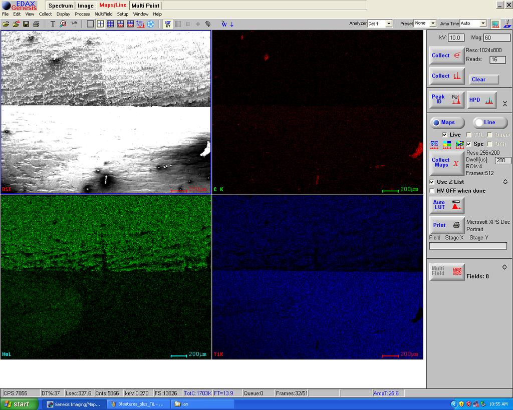
7 EDS or WDS: count the events within a given peak window and map beam position when each event occurs A Guide to Energy Dispersive X-Ray Analysis p.13 Mapping Because most of your samples are NOT flat smooth / polished homogeneous p.14 7

8 Trading peak resolution for data collection rates A Guide to Energy Dispersive X-Ray Analysis p.15 p.16 8


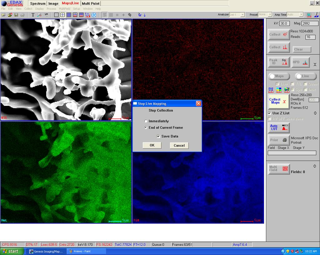
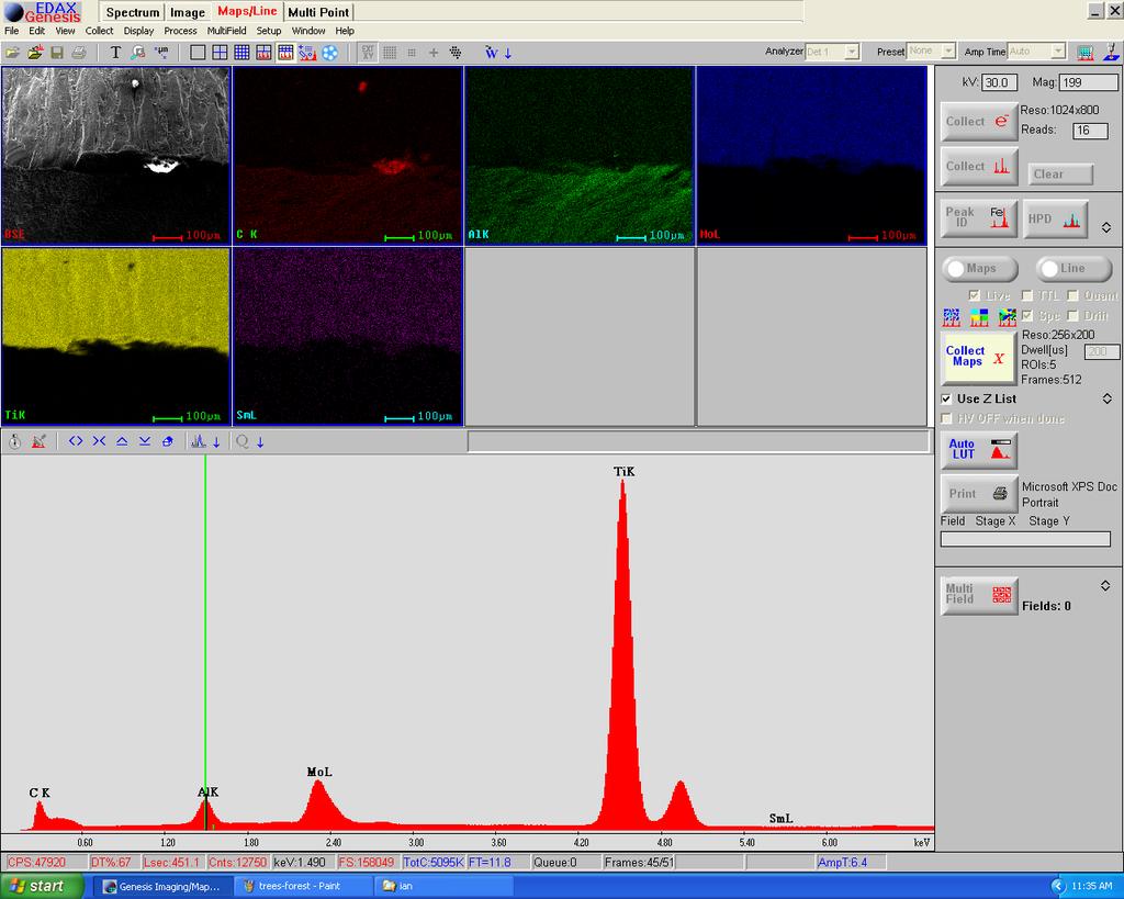
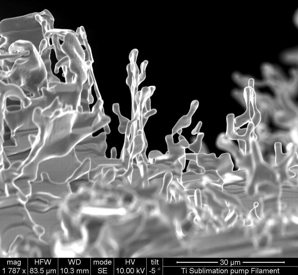
9 Ti Sub ion pump filament p.17 Hoar frost : Take a nice picture first p.18 9

10 Use a background window p.19 after letting it run for ~10 minutes p.20 10

11 p.21 p.22 11

12 setup p.23 Collect Maps p.24 12

13 p.25 End collection, release ext p.26 13


14 p.27 p.28 14

15 p.29 p.30 15

16 p.31 p.32 16

17 p.33 Run at hi V acc to identify all peaks look for relevant L, M do you need better resolution? How to analyze thin organic film? Drop V acc Tilt the sample p.34 17
, primary Sn phase")


18 SEM (BSE) view of gross residual BCB (DOA) BSE (Z-sensitive) image shows dramatic contrast between organic (dark), primary Sn phase (grey), and primary Pb phase (white) p.35 Miscellaneous Failure Mechanisms: Assembly Solderability 5x5 750/500 TC test First failure at ~150 cycles (Ni/Au only) Catastrophic failure rate on affected boards Unknown source of process sensitivity Solder lift-off from pad Adjacent good pad p.36 18


")

19 EDS Maps of a Typical Pad Interface (Where-n-tar-blazes did the Cu come from??) BSE image Ni map Cu map p.37 Typical Ni/Au device (post-polish / 50% nitric; 3 min. decorative etch) Etched bulk eutectic solder Cu/Sn intermetallic Columnar Ni grains Etched Cu pad p.38 19


20 EDS Maps of a Failed Pad Interface (note lack of Cu/Sn intermetallic) p.39 XRF: X-Ray Fluorescence p.40 20


21 XRF: High Sensitivity vs. SEM-based Bulk analysis technique Lower spatial resolution (mm-mapping) non-vacuum or low vacuum quantitation; liquids possible Reduced background p.41 Microspot XRF (June) p.42 21


22 Spectral Mapping - Bone Fossilization Fe K P Si Na p.43 Map Image Overlays: Bone Fossilization Fe Red K Blue Si Yellow P Gray Na - Green p.44 22
MT Electron microscopy Scanning electron microscopy and electron probe microanalysis
 MT-0.6026 Electron microscopy Scanning electron microscopy and electron probe microanalysis Eero Haimi Research Manager Outline 1. Introduction Basics of scanning electron microscopy (SEM) and electron
Electron probe microanalysis - Electron microprobe analysis EPMA (EMPA) What s EPMA all about? What can you learn?
 What s EPMA all about? What can you learn?") Electron probe microanalysis - Electron microprobe analysis EPMA (EMPA) What s EPMA all about? What can you learn? EPMA - what is it? Precise and accurate quantitative chemical analyses of micron-size
Electron probe microanalysis - Electron microprobe analysis EPMA (EMPA) What s EPMA all about? What can you learn? EPMA - what is it? Precise and accurate quantitative chemical analyses of micron-size
SEM. Chemical Analysis in the. Elastic and Inelastic scattering. Chemical analysis in the SEM. Chemical analysis in the SEM
 THE UNIVERSITY Chemical Analysis in the SEM Ian Jones Centre for Electron Microscopy OF BIRMINGHAM Elastic and Inelastic scattering Electron interacts with one of the orbital electrons Secondary electrons,
HOW TO APPROACH SCANNING ELECTRON MICROSCOPY AND ENERGY DISPERSIVE SPECTROSCOPY ANALYSIS. SCSAM Short Course Amir Avishai
 HOW TO APPROACH SCANNING ELECTRON MICROSCOPY AND ENERGY DISPERSIVE SPECTROSCOPY ANALYSIS SCSAM Short Course Amir Avishai RESEARCH QUESTIONS Sea Shell Cast Iron EDS+SE Fe Cr C Objective Ability to ask the
MS482 Materials Characterization ( 재료분석 ) Lecture Note 4: XRF
 Lecture Note 4: XRF") 2016 Fall Semester MS482 Materials Characterization ( 재료분석 ) Lecture Note 4: XRF Byungha Shin Dept. of MSE, KAIST 1 Course Information Syllabus 1. Overview of various characterization techniques (1 lecture)
2016 Fall Semester MS482 Materials Characterization ( 재료분석 ) Lecture Note 4: XRF Byungha Shin Dept. of MSE, KAIST 1 Course Information Syllabus 1. Overview of various characterization techniques (1 lecture)
Technical University of Denmark. Center for Electron Nanoscopy. Advanced TEM (16 September 2010) Microanalysis in the electron microscope
 Microanalysis in the electron microscope") Microanalysis in the electron microscope MH1 1 Technical University of Denmark Center for Electron Nanoscopy Advanced TEM (16 September 2010) Microanalysis in the electron microscope Dr C B Boothroyd Synopsis
Microanalysis in the electron microscope MH1 1 Technical University of Denmark Center for Electron Nanoscopy Advanced TEM (16 September 2010) Microanalysis in the electron microscope Dr C B Boothroyd Synopsis
EDS User School. Principles of Electron Beam Microanalysis
 EDS User School Principles of Electron Beam Microanalysis Outline 1.) Beam-specimen interactions 2.) EDS spectra: Origin of Bremsstrahlung and characteristic peaks 3.) Moseley s law 4.) Characteristic
Understanding X-rays: The electromagnetic spectrum
 Understanding X-rays: The electromagnetic spectrum 1 ULa 13.61 kev 0.09 nm BeKa 0.11 kev 11.27 nm E = hn = h c l where, E : energy, h : Planck's constant, n : frequency c : speed of light in vacuum, l
ECE Semiconductor Device and Material Characterization
 ECE 4813 Semiconductor Device and Material Characterization Dr. Alan Doolittle School of Electrical and Computer Engineering Georgia Institute of Technology As with all of these lecture slides, I am indebted
Silicon Drift Detectors: Understanding the Advantages for EDS Microanalysis. Patrick Camus, PhD Applications Scientist March 18, 2010
 Silicon Drift Detectors: Understanding the Advantages for EDS Microanalysis Patrick Camus, PhD Applications Scientist March 18, 2010 EDS Detector Requirements Detect whole energy range of x-rays 50 ev
Praktikum zur. Materialanalytik
 Praktikum zur Materialanalytik Energy Dispersive X-ray Spectroscopy B513 Stand: 19.10.2016 Contents 1 Introduction... 2 2. Fundamental Physics and Notation... 3 2.1. Alignments of the microscope... 3 2.2.
Understanding X-rays: The electromagnetic spectrum
 Understanding X-rays: The electromagnetic spectrum 1 ULa 13.61 kev 0.09 nm BeKa 0.11 kev 11.27 nm E = hn = h c l where, E : energy, h : Planck's constant, n : frequency c : speed of light in vacuum, l
ABC s of Electrochemistry series Materials Characterization techniques: SEM and EDS Ana María Valenzuela-Muñiz November 3, 2011
 ABC s of Electrochemistry series Materials Characterization techniques: SEM and EDS Ana María Valenzuela-Muñiz November 3, 2011 CEER, Department of Chemical and Biomolecular Engineering Outline Introduction
Contrasted strengths and weakness of EDS, WDS and AES for determining the composition of samples
 Contrasted strengths and weakness of EDS, WDS and AES for determining the composition of samples Ana-Marija Nedić Course 590B 12/07/2018 Iowa State University Contrasted strengths and weakness of EDS,
Chemical Analysis in TEM: XEDS, EELS and EFTEM. HRTEM PhD course Lecture 5
 Chemical Analysis in TEM: XEDS, EELS and EFTEM HRTEM PhD course Lecture 5 1 Part IV Subject Chapter Prio x-ray spectrometry 32 1 Spectra and mapping 33 2 Qualitative XEDS 34 1 Quantitative XEDS 35.1-35.4
6. Analytical Electron Microscopy
 Physical Principles of Electron Microscopy 6. Analytical Electron Microscopy Ray Egerton University of Alberta and National Institute of Nanotechnology Edmonton, Canada www.tem-eels.ca regerton@ualberta.ca
Auger Electron Spectroscopy
 Auger Electron Spectroscopy Auger Electron Spectroscopy is an analytical technique that provides compositional information on the top few monolayers of material. Detect all elements above He Detection
Overview of X-Ray Fluorescence Analysis
 Overview of X-Ray Fluorescence Analysis AMPTEK, INC., Bedford, MA 01730 Ph: +1 781 275 2242 Fax: +1 781 275 3470 sales@amptek.com 1 What is X-Ray Fluorescence (XRF)? A physical process: Emission of characteristic
Modern Optical Spectroscopy
 Modern Optical Spectroscopy X-Ray Microanalysis Shu-Ping Lin, Ph.D. Institute of Biomedical Engineering E-mail: splin@dragon.nchu.edu.tw Website: http://web.nchu.edu.tw/pweb/users/splin/ Backscattered
Detection of X-Rays. Solid state detectors Proportional counters Microcalorimeters Detector characteristics
 Detection of X-Rays Solid state detectors Proportional counters Microcalorimeters Detector characteristics Solid State X-ray Detectors X-ray interacts in material to produce photoelectrons which are collected
X-ray Microanalysis in Nanomaterials
 3 X-ray Microanalysis in Nanomaterials Robert Anderhalt 1. Introduction Traditionally, energy dispersive x-ray spectroscopy (EDS) in the scanning electron microscope (SEM) has been called microanalysis,
MICRO-TOMOGRAPHY AND X-RAY ANALYSIS OF GEOLOGICAL SAMPLES
 THE PUBLISHING HOUSE PROCEEDINGS OF THE ROMANIAN ACADEMY, Series A, OF THE ROMANIAN ACADEMY Volume 18, Number 1/2017, pp. 42 49 MICRO-TOMOGRAPHY AND X-RAY ANALYSIS OF GEOLOGICAL SAMPLES Ion GRUIA University
X-Ray Fluorescence and Natural History
 X-Ray Fluorescence and Natural History How XRF Helps XRF can be used both quantitatively (homogenous samples) and quantitatively (heterogenous samples).! Trace elements in a fossil can help identify source,
Electron Microprobe Analysis and Scanning Electron Microscopy
 Electron Microprobe Analysis and Scanning Electron Microscopy Electron microprobe analysis (EMPA) Analytical technique in which a beam of electrons is focused on a sample surface, producing X-rays from
CHEM-E5225 :Electron Microscopy X-Ray Spectrometry
 CHEM-E5225 :Electron Microscopy X-Ray Spectrometry 2016.11 Yanling Ge Outline X-ray Spectrometry X-ray Spectra and Images Qualitative and Quantitative X-ray Analysis and Imaging Discussion of homework
BENEFITS OF IMPROVED RESOLUTION FOR EDXRF
 135 Abstract BENEFITS OF IMPROVED RESOLUTION FOR EDXRF R. Redus 1, T. Pantazis 1, J. Pantazis 1, A. Huber 1, B. Cross 2 1 Amptek, Inc., 14 DeAngelo Dr, Bedford MA 01730, 781-275-2242, www.amptek.com 2
hν' Φ e - Gamma spectroscopy - Prelab questions 1. What characteristics distinguish x-rays from gamma rays? Is either more intrinsically dangerous?
 Gamma spectroscopy - Prelab questions 1. What characteristics distinguish x-rays from gamma rays? Is either more intrinsically dangerous? 2. Briefly discuss dead time in a detector. What factors are important
MT Electron microscopy Scanning electron microscopy and electron probe microanalysis
 MT-0.6026 Electron microscopy Scanning electron microscopy and electron probe microanalysis Eero Haimi Research Manager Outline 1. Introduction Basics of scanning electron microscopy (SEM) and electron
MSE 321 Structural Characterization
 Auger Spectroscopy Auger Electron Spectroscopy (AES) Scanning Auger Microscopy (SAM) Incident Electron Ejected Electron Auger Electron Initial State Intermediate State Final State Physical Electronics
EPMA IMAGES. Figure 9. Energy-dispersive spectra of spot mineral analyses in sample 89GGR-33A for locations 1-5 in Figure 8.
 EPMA IMAGES The attached images and mineral data can be used to supplement an instrument-based lab, or serve as the basis for lab that can be completed without an instrument. Please provide credit for
Detecting high energy photons. Interactions of photons with matter Properties of detectors (with examples)
") Detecting high energy photons Interactions of photons with matter Properties of detectors (with examples) Interactions of high energy photons with matter Cross section/attenution length/optical depth Photoelectric
Detecting high energy photons Interactions of photons with matter Properties of detectors (with examples) Interactions of high energy photons with matter Cross section/attenution length/optical depth Photoelectric
Development of Gamma-ray Monitor using CdZnTe Semiconductor Detector
 Development of Gamma-ray Monitor using CdZnTe Semiconductor Detector A. H. D. Rasolonjatovo 1, T. Shiomi 1, T. Nakamura 1 Y. Tsudaka 2, H. Fujiwara 2, H. Araki 2, K. Matsuo 2, H. Nishizawa 2 1 Cyclotron
Diffractometer. Geometry Optics Detectors
 Diffractometer Geometry Optics Detectors Diffractometers Debye Scherrer Camera V.K. Pecharsky and P.Y. Zavalij Fundamentals of Powder Diffraction and Structural Characterization of Materials. Diffractometers
Generation of X-Rays in the SEM specimen
 Generation of X-Rays in the SEM specimen The electron beam generates X-ray photons in the beam-specimen interaction volume beneath the specimen surface. Some X-ray photons emerging from the specimen have
MS482 Materials Characterization ( 재료분석 ) Lecture Note 5: RBS
 Lecture Note 5: RBS") 2016 Fall Semester MS482 Materials Characterization ( 재료분석 ) Lecture Note 5: RBS Byungha Shin Dept. of MSE, KAIST 1 Course Information Syllabus 1. Overview of various characterization techniques (1 lecture)
2016 Fall Semester MS482 Materials Characterization ( 재료분석 ) Lecture Note 5: RBS Byungha Shin Dept. of MSE, KAIST 1 Course Information Syllabus 1. Overview of various characterization techniques (1 lecture)
Improvements for Absorption Spectroscopy at Beamlines A1, E4, X1
 Improvements for Absorption Spectroscopy at Beamlines A1, E4, X1 U. Brüggmann 1, N. Haack, M. Herrmann 2, S.K.J. Johnas 3, P. Kappen, K. Klementiev 4, E. Welter For an improvement of the conditions of
X Rays & Crystals. Characterizing Mineral Chemistry & Structure. J.D. Price
 X Rays & Crystals Characterizing Mineral Chemistry & Structure J.D. Price Light - electromagnetic spectrum Wave behavior vs. particle behavior If atoms are on the 10-10 m scale, we need to use sufficiently
Chemistry 311: Instrumentation Analysis Topic 2: Atomic Spectroscopy. Chemistry 311: Instrumentation Analysis Topic 2: Atomic Spectroscopy
 Topic 2b: X-ray Fluorescence Spectrometry Text: Chapter 12 Rouessac (1 week) 4.0 X-ray Fluorescence Download, read and understand EPA method 6010C ICP-OES Winter 2009 Page 1 Atomic X-ray Spectrometry Fundamental
Gaetano L Episcopo. Scanning Electron Microscopy Focus Ion Beam and. Pulsed Plasma Deposition
 Gaetano L Episcopo Scanning Electron Microscopy Focus Ion Beam and Pulsed Plasma Deposition Hystorical background Scientific discoveries 1897: J. Thomson discovers the electron. 1924: L. de Broglie propose
Semiconductor X-Ray Detectors. Tobias Eggert Ketek GmbH
 Semiconductor X-Ray Detectors Tobias Eggert Ketek GmbH Semiconductor X-Ray Detectors Part A Principles of Semiconductor Detectors 1. Basic Principles 2. Typical Applications 3. Planar Technology 4. Read-out
X-ray Spectroscopy. Interaction of X-rays with matter XANES and EXAFS XANES analysis Pre-edge analysis EXAFS analysis
 X-ray Spectroscopy Interaction of X-rays with matter XANES and EXAFS XANES analysis Pre-edge analysis EXAFS analysis Element specific Sensitive to low concentrations (0.01-0.1 %) Why XAS? Applicable under
Swanning about in Reciprocal Space. Kenneth, what is the wavevector?
 Swanning about in Reciprocal Space or, Kenneth, what is the wavevector? Stanford Synchrotron Radiation Laboratory Principles The relationship between the reciprocal lattice vector and the wave vector is
Hybrid Wafer Level Bonding for 3D IC
 Hybrid Wafer Level Bonding for 3D IC An Equipment Perspective Markus Wimplinger, Corporate Technology Development & IP Director History & Roadmap - BSI CIS Devices???? 2013 2 nd Generation 3D BSI CIS with
Electron Microprobe Analysis 1 Nilanjan Chatterjee, Ph.D. Principal Research Scientist
 12.141 Electron Microprobe Analysis 1 Nilanjan Chatterjee, Ph.D. Principal Research Scientist Massachusetts Institute of Technology Electron Microprobe Facility Department of Earth, Atmospheric and Planetary
Electron Microprobe Analysis 1 Nilanjan Chatterjee, Ph.D. Principal Research Scientist
 12.141 Electron Microprobe Analysis 1 Nilanjan Chatterjee, Ph.D. Principal Research Scientist Massachusetts Institute of Technology Electron Microprobe Facility Department of Earth, Atmospheric and Planetary
Introduction to EDX. Energy Dispersive X-ray Microanalysis (EDS, Energy dispersive Spectroscopy) Basics of EDX
 Basics of EDX") Introduction to EDX Energy Dispersive X-ray Microanalysis (EDS, Energy dispersive Spectroscopy) EDX Marco Cantoni 1 Basics of EDX a) Generation of X-rays b) Detection Si(Li) Detector, SDD Detector, EDS
Introduction to EDX Energy Dispersive X-ray Microanalysis (EDS, Energy dispersive Spectroscopy) EDX Marco Cantoni 1 Basics of EDX a) Generation of X-rays b) Detection Si(Li) Detector, SDD Detector, EDS
A Photonic Crystal Laser from Solution Based. Organo-Lead Iodide Perovskite Thin Films
 SUPPORTING INFORMATION A Photonic Crystal Laser from Solution Based Organo-Lead Iodide Perovskite Thin Films Songtao Chen 1, Kwangdong Roh 2, Joonhee Lee 1, Wee Kiang Chong 3,4, Yao Lu 5, Nripan Mathews
Spectroscopy of Nanostructures. Angle-resolved Photoemission (ARPES, UPS)
") Spectroscopy of Nanostructures Angle-resolved Photoemission (ARPES, UPS) Measures all quantum numbers of an electron in a solid. E, k x,y, z, point group, spin E kin, ϑ,ϕ, hν, polarization, spin Electron
Spectroscopy of Nanostructures Angle-resolved Photoemission (ARPES, UPS) Measures all quantum numbers of an electron in a solid. E, k x,y, z, point group, spin E kin, ϑ,ϕ, hν, polarization, spin Electron
Auger Electron Spectroscopy Overview
 Auger Electron Spectroscopy Overview Also known as: AES, Auger, SAM 1 Auger Electron Spectroscopy E KLL = E K - E L - E L AES Spectra of Cu EdN(E)/dE Auger Electron E N(E) x 5 E KLL Cu MNN Cu LMM E f E
Chem 481 Lecture Material 3/20/09
 Chem 481 Lecture Material 3/20/09 Radiation Detection and Measurement Semiconductor Detectors The electrons in a sample of silicon are each bound to specific silicon atoms (occupy the valence band). If
Peter L Warren, Pamela Y Shadforth ICI Technology, Wilton, Middlesbrough, U.K.
 783 SCOPE AND LIMITATIONS XRF ANALYSIS FOR SEMI-QUANTITATIVE Introduction Peter L Warren, Pamela Y Shadforth ICI Technology, Wilton, Middlesbrough, U.K. Historically x-ray fluorescence spectrometry has
Application of the GD-Profiler 2 to the PV domain
 Application of the GD-Profiler 2 to the PV domain GD Profiler 2 RF GDOES permits to follow the distribution of the elements as function of depth. This is an ultra fast characterisation technique capable
Single Photon detectors
 Single Photon detectors Outline Motivation for single photon detection Semiconductor; general knowledge and important background Photon detectors: internal and external photoeffect Properties of semiconductor
NUCLEAR TRANSMUTATION IN DEUTERED PD FILMS IRRADIATED BY AN UV LASER
 Castellano, et al. Nuclear Transmutation in Deutered Pd Films Irradiated by an UV Laser. in 8th International Conference on Cold Fusion. 2000. Lerici (La Spezia), Italy: Italian Physical Society, Bologna,
Interactions with Matter
 Manetic Lenses Manetic fields can displace electrons Manetic field can be produced by passin an electrical current throuh coils of wire Manetic field strenth can be increased by usin a soft ferromanetic
MODERN OPTICS. P47 Optics: Unit 9
 MODERN OPTICS P47 Optics: Unit 9 Course Outline Unit 1: Electromagnetic Waves Unit 2: Interaction with Matter Unit 3: Geometric Optics Unit 4: Superposition of Waves Unit 5: Polarization Unit 6: Interference
Geology 777 Monte Carlo Exercise I
 Geology 777 Monte Carlo Exercise I Purpose The goal of this exercise is to get you to think like an electron... to start to think about where electrons from the stream of high energy electrons go when
TIMEPIX3 First measurements and characterization of a hybrid pixel detector working in event driven mode
 TIMEPIX3 First measurements and characterization of a hybrid pixel detector working in event driven mode Erik Fröjdh 1,2, Michael Campbell 2, Massimiliano de Gaspari 2, Szymon Kulis 2, Xavier Llopart 2,
Science Lab I Properties of Light
 Art & Science of Light Fall 2007 Science Lab I Properties of Light Prepared by: Dr. Dharshi Bopegedera 1 Using the Filtergraph (15 minutes) 1. Turn on the filtergraph, place a card on it and look at the
Pulse Height Analysis System (PHA) designed for W7-X Presented by Monika KUBKOWSKA
 designed for W7-X Presented by Monika KUBKOWSKA") Pulse Height Analysis System (PHA) designed for W7-X Presented by Monika KUBKOWSKA This scientific work has been partly supported by Polish Ministry of Science and Higher Education within the framework
Pulse Height Analysis System (PHA) designed for W7-X Presented by Monika KUBKOWSKA This scientific work has been partly supported by Polish Ministry of Science and Higher Education within the framework
Electron Probe Microanalysis (EPMA)
") Electron Probe Microanalysis (EPMA) By John J. Donovan (portions from J. I. Goldstein, D. E. Newbury, P. Echlin, D. C. Joy, C. Fiori, E. Lifshin, "Scanning Electron Microscopy and X-Ray Microanalysis",
Electron Probe Microanalysis (EPMA) By John J. Donovan (portions from J. I. Goldstein, D. E. Newbury, P. Echlin, D. C. Joy, C. Fiori, E. Lifshin, "Scanning Electron Microscopy and X-Ray Microanalysis",
5.8 Auger Electron Spectroscopy (AES)
") 5.8 Auger Electron Spectroscopy (AES) 5.8.1 The Auger Process X-ray and high energy electron bombardment of atom can create core hole Core hole will eventually decay via either (i) photon emission (x-ray
5.8 Auger Electron Spectroscopy (AES) 5.8.1 The Auger Process X-ray and high energy electron bombardment of atom can create core hole Core hole will eventually decay via either (i) photon emission (x-ray
Lecture 5-8 Instrumentation
 Lecture 5-8 Instrumentation Requirements 1. Vacuum Mean Free Path Contamination Sticking probability UHV Materials Strength Stability Permeation Design considerations Pumping speed Virtual leaks Leaking
Standards-Based Quantification in DTSA-II Part I
 Part I Nicholas W.M. Ritchie National Institute of Standards and Technology, Gaithersburg, MD 20899-8371 nicholas.ritchie@nist.gov Introduction Quantifying an X-ray spectrum is the process of converting
Mass Determination of Rn and Hg isotopes using MASHA
 Mass Determination of Rn and Hg isotopes using MASHA Alfred M. Sehone Lumkile Msebi Oleg Lishyk Stanislav Stanishevski Yuliya Brechko Supervisor Krupa Lubosh Flerov Laboratory of Nuclear reactions, JINR,
Chapter 4 Scintillation Detectors
 Med Phys 4RA3, 4RB3/6R03 Radioisotopes and Radiation Methodology 4-1 4.1. Basic principle of the scintillator Chapter 4 Scintillation Detectors Scintillator Light sensor Ionizing radiation Light (visible,
International Journal of Scientific & Engineering Research, Volume 5, Issue 3, March-2014 ISSN
 316 Effective atomic number of composite materials by Compton scattering - nondestructive evaluation method Kiran K U a, Ravindraswami K b, Eshwarappa K M a and Somashekarappa H M c* a Government Science
MS482 Materials Characterization ( 재료분석 ) Lecture Note 12: Summary. Byungha Shin Dept. of MSE, KAIST
 Lecture Note 12: Summary. Byungha Shin Dept. of MSE, KAIST") 2015 Fall Semester MS482 Materials Characterization ( 재료분석 ) Lecture Note 12: Summary Byungha Shin Dept. of MSE, KAIST 1 Course Information Syllabus 1. Overview of various characterization techniques (1
2015 Fall Semester MS482 Materials Characterization ( 재료분석 ) Lecture Note 12: Summary Byungha Shin Dept. of MSE, KAIST 1 Course Information Syllabus 1. Overview of various characterization techniques (1
Surface Sensitivity & Surface Specificity
 Surface Sensitivity & Surface Specificity The problems of sensitivity and detection limits are common to all forms of spectroscopy. In its simplest form, the question of sensitivity boils down to whether
AGATA preamplifier performance on large signals from a 241 Am+Be source. F. Zocca, A. Pullia, D. Bazzacco, G. Pascovici
 AGATA preamplifier performance on large signals from a 241 Am+Be source F. Zocca, A. Pullia, D. Bazzacco, G. Pascovici AGATA Week - LNL (PD), Italy, 12-15 November 2007 Outline Recalls : Fast reset device
Everhart-Thornley detector
 SEI Detector Everhart-Thornley detector Microscope chamber wall Faraday cage Scintillator Electrons in Light pipe Photomultiplier Electrical signal out Screen Quartz window +200 V +10 kv Always contains
SUPPLEMENTARY MATERIALS FOR PHONON TRANSMISSION COEFFICIENTS AT SOLID INTERFACES
 148 A p p e n d i x D SUPPLEMENTARY MATERIALS FOR PHONON TRANSMISSION COEFFICIENTS AT SOLID INTERFACES D.1 Overview The supplementary information contains additional information on our computational approach
Electrochromic Metallo-Organic Nanoscale Films: Fabrication, Color Range, and Devices
 Electrochromic Metallo-Organic Nanoscale Films: Fabrication, Color Range, and Devices Neta Elool Dov, 1 Sreejith Shankar, 1 Dana Cohen, 1 Tatyana Bendikov, 2 Katya Rechav, 2 Linda J. W. Shimon, 2 Michal
ECE Semiconductor Device and Material Characterization
 ECE 4813 Semiconductor Device and Material Characterization Dr. Alan Doolittle School of Electrical and Computer Engineering Georgia Institute of Technology As with all of these lecture slides, I am indebted
Development of a new MeV gamma-ray camera
 Development of a new MeV gamma-ray camera ICEPP Symposium February 16, 2004 Hakuba, Nagano, Japan Kyoto University Atsushi Takeda H. Kubo, K. Miuchi, T. Nagayoshi, Y. Okada, R. Orito, A. Takada, T. Tanimori,
Chapter 9. Electron mean free path Microscopy principles of SEM, TEM, LEEM
 Chapter 9 Electron mean free path Microscopy principles of SEM, TEM, LEEM 9.1 Electron Mean Free Path 9. Scanning Electron Microscopy (SEM) -SEM design; Secondary electron imaging; Backscattered electron
Gamma and X-Ray Detection
 Gamma and X-Ray Detection DETECTOR OVERVIEW The kinds of detectors commonly used can be categorized as: a. Gas-filled Detectors b. Scintillation Detectors c. Semiconductor Detectors The choice of a particular
GEM at CERN. Leszek Ropelewski CERN PH-DT2 DT2-ST & TOTEM
 GEM at CERN Leszek Ropelewski CERN PH-DT2 DT2-ST & TOTEM MicroStrip Gas Chamber Semiconductor industry technology: Photolithography Etching Coating Doping A. Oed Nucl. Instr. and Meth. A263 (1988) 351.
Chemistry 524--Final Exam--Keiderling Dec. 12, pm SES
 Chemistry 524--Final Exam--Keiderling Dec. 12, 2002 --4-8 pm -- 238 SES Please answer all questions in the answer book provided. Calculators, rulers, pens and pencils are permitted plus one 8.5 x 11 sheet
Chemistry Instrumental Analysis Lecture 19 Chapter 12. Chem 4631
 Chemistry 4631 Instrumental Analysis Lecture 19 Chapter 12 There are three major techniques used for elemental analysis: Optical spectrometry Mass spectrometry X-ray spectrometry X-ray Techniques include:
Auger Electron Spectroscopy (AES) Prof. Paul K. Chu
 Prof. Paul K. Chu") Auger Electron Spectroscopy (AES) Prof. Paul K. Chu Auger Electron Spectroscopy Introduction Principles Instrumentation Qualitative analysis Quantitative analysis Depth profiling Mapping Examples The Auger
Auger Electron Spectroscopy (AES) Prof. Paul K. Chu Auger Electron Spectroscopy Introduction Principles Instrumentation Qualitative analysis Quantitative analysis Depth profiling Mapping Examples The Auger
Radiation Detection and Measurement
 Radiation Detection and Measurement June 2008 Tom Lewellen Tkldog@u.washington.edu Types of radiation relevant to Nuclear Medicine Particle Symbol Mass (MeV/c 2 ) Charge Electron e-,! - 0.511-1 Positron
XUV 773: X-Ray Fluorescence Analysis of Gemstones
 Fischer Application report vr118 HELM UT FISCHER GMBH + CO. KG Institut für Elektronik und Messtechnik Industriestrasse 21-7169 Sindelfingen, Germany Tel.: (+49) 731 33- - Fax: (+49) 731 33-79 E-Mail:
Developments & Limitations in GSR Analysis
 Developments & Limitations in GSR Analysis ENFSI Working Group Meeting June 2006 Jenny Goulden Oxford Instruments NanoAnalysis Overview Introduction Developments in GSR Software Importance of EDS Hardware
MS482 Materials Characterization ( 재료분석 ) Lecture Note 2: UPS
 Lecture Note 2: UPS") 2016 Fall Semester MS482 Materials Characterization ( 재료분석 ) Lecture Note 2: UPS Byungha Shin Dept. of MSE, KAIST 1 Course Information Syllabus 1. Overview of various characterization techniques (1 lecture)
2016 Fall Semester MS482 Materials Characterization ( 재료분석 ) Lecture Note 2: UPS Byungha Shin Dept. of MSE, KAIST 1 Course Information Syllabus 1. Overview of various characterization techniques (1 lecture)
CALCULATION OF THE DETECTOR-CONTRIBUTION TO ZIRCONIUM PEAKS IN EDXRF SPECTRA OBTAINED WITH A SI-DRIFT DETECTOR
 CALCULATION OF THE DETECTOR-CONTRIBUTION TO ZIRCONIUM PEAKS IN EDXRF SPECTRA OBTAINED WITH A SI-DRIFT DETECTOR A. C. Neiva 1, J. N. Dron 1, L. B. Lopes 1 1 Escola Politécnica da Universidade de São Paulo
Development and optimization of scanning micro-xrf instrumentation using monochromatic excitation
 Department of Analytical Chemistry X-Ray Microspectroscopy and Imaging Development and optimization of scanning micro-xrf instrumentation using monochromatic excitation Thesis submitted to obtain the degree
Analysis of γ spectrum
 IFM The Department of Physics, Chemistry and Biology LAB 26 Analysis of γ spectrum NAME PERSONAL NUMBER DATE APPROVED I. OBJECTIVES - To understand features of gamma spectrum and recall basic knowledge
Exploiting the Speed of the Silicon Drift Detector to Open New Measurement Opportunities in Particle Analysis. Dale E. Newbury
 Exploiting the Speed of the Silicon Drift Detector to Open New Measurement Opportunities in Particle Analysis Dale E. Newbury National Institute of Standards and Technology Gaithersburg, MD 20899-8370
XRF books: Analytical Chemistry, Kellner/Mermet/Otto/etc. 3 rd year XRF Spectroscopy Dr. Alan Ryder (R222, Physical Chemistry) 2 lectures:
 2 lectures:") 1 3 rd year XRF Spectroscopy Dr. Alan Ryder (R222, Physical Chemistry) 2 lectures: XRF spectroscopy 1 exam question. Notes on: www.nuigalway.ie/nanoscale/3rdspectroscopy.html XRF books: Analytical Chemistry,
1 3 rd year XRF Spectroscopy Dr. Alan Ryder (R222, Physical Chemistry) 2 lectures: XRF spectroscopy 1 exam question. Notes on: www.nuigalway.ie/nanoscale/3rdspectroscopy.html XRF books: Analytical Chemistry,
The X-Ray Universe. Potsdam University. Dr. Lidia Oskinova Wintersemester 2008/09
 The X-Ray Universe The X-Ray Universe Potsdam University Dr. Lidia Oskinova Wintersemester 2008/09 lida@astro.physik.uni-potsdam.de astro.physik.uni-potsdam.de/~lida/x-ray.html Chandra X-ray Observatory
Chemical Analysis. Energy Dispersive X-Ray Spectroscopy (EDS)
") Chemical Analysis We have so far discussed several of the signals detected on interaction of a high-energy electron beam with a solid sample (secondary, backscattered, transmitted, and diffracted electrons);
Chemical Analysis We have so far discussed several of the signals detected on interaction of a high-energy electron beam with a solid sample (secondary, backscattered, transmitted, and diffracted electrons);
Setting The motor that rotates the sample about an axis normal to the diffraction plane is called (or ).
.") X-Ray Diffraction X-ray diffraction geometry A simple X-ray diffraction (XRD) experiment might be set up as shown below. We need a parallel X-ray source, which is usually an X-ray tube in a fixed position
X-Ray Diffraction X-ray diffraction geometry A simple X-ray diffraction (XRD) experiment might be set up as shown below. We need a parallel X-ray source, which is usually an X-ray tube in a fixed position
Electron Microscopy I
 Characterization of Catalysts and Surfaces Characterization Techniques in Heterogeneous Catalysis Electron Microscopy I Introduction Properties of electrons Electron-matter interactions and their applications
Supplementary Figure 1. A photographic image of directionally grown perovskite films on a glass substrate (size: cm).
.") Supplementary Figure 1. A photographic image of directionally grown perovskite films on a glass substrate (size: 1.5 4.5 cm). 1 Supplementary Figure 2. Optical microscope images of MAPbI 3 films formed
Supplementary Figure 1. A photographic image of directionally grown perovskite films on a glass substrate (size: 1.5 4.5 cm). 1 Supplementary Figure 2. Optical microscope images of MAPbI 3 films formed
Superconducting Single-photon Detectors
 : Quantum Cryptography Superconducting Single-photon Detectors Hiroyuki Shibata Abstract This article describes the fabrication and properties of a single-photon detector made of a superconducting NbN
The first model was based only on the CANBERRA information which we. drawing. Canberra refused any other information.
 Experimental and Monte Carlo determination of Gamma Spectrometry Efficiency Pavel Dryak, Petr Kovář Czech Metrology Institute February 2009 Leading motive of our testing The producer send the drawing after
Basics of Synchrotron Radiation Beamlines and Detectors. Basics of synchrotron radiation X-ray optics as they apply to EXAFS experiments Detectors
 Basics of Synchrotron Radiation Beamlines and Detectors Basics of synchrotron radiation X-ray optics as they apply to EXAFS experiments Detectors Important properties of Synchrotron Radiation Tunability
CHEM*3440. X-Ray Energies. Bremsstrahlung Radiation. X-ray Line Spectra. Chemical Instrumentation. X-Ray Spectroscopy. Topic 13
 X-Ray Energies very short wavelength radiation 0.1Å to 10 nm (100 Å) CHEM*3440 Chemical Instrumentation Topic 13 X-Ray Spectroscopy Visible - Ultraviolet (UV) - Vacuum UV (VUV) - Extreme UV (XUV) - Soft
= 6 (1/ nm) So what is probability of finding electron tunneled into a barrier 3 ev high?
 So what is probability of finding electron tunneled into a barrier 3 ev high?") STM STM With a scanning tunneling microscope, images of surfaces with atomic resolution can be readily obtained. An STM uses quantum tunneling of electrons to map the density of electrons on the surface
STM STM With a scanning tunneling microscope, images of surfaces with atomic resolution can be readily obtained. An STM uses quantum tunneling of electrons to map the density of electrons on the surface