RASTROVACIA SONDOVÁ MIKROSKOPIA
|
|
|
- Jayson Glenn
- 6 years ago
- Views:
Transcription
1 Katedra experimentálnej fyziky Fakulta matematiky, fyziky a informatiky UNIVERZITA KOMENSKÉHO V BRATISLAVE RASTROVACIA SONDOVÁ MIKROSKOPIA Prof.RNDr. Andrej PLECENIK, DrSc.
2 Obsah prednášky História tunelového javu Od tunelového javu k Rastrovaciemu tunelovému mikroskopu Princíp Rastrovacieho tunelového mikroskopu Rozdelenie Rastrovacích tunelových mikroskopov Meranie lokálnej hustoty stavov Rastrovacie silové mikroskopy ich princípy AFM, EFM, MFM,... SNOM Využitie SPM v litografii
3 Pravdepodobnosť prechodu elektrónu cez potenciálovú bariéru [ ] 2 1/ 2 1/ ) ( 2 ), ( ), ( ) ( x x d x K x E x V m E x dx E x K Me E D = = = α α TUNELOVÝ JAV
4 y N 1 I N 2 z x ~ N 1 ( E ev ) f ( E ev )de ~ N 2 [ ]de ( E) 1 f ( E) j = en v f ( E) = 1 1+ e E E kt F je Fermiho rozdelovacia funkcia j = de D( E ) de N1( E) N2( E ev) ) π me h { f ( E) f ( E ev }
 = E exp( k 1 E f ) + 1")
5 Hustota stavov N E = dn de V 2π 3 / 2 1/ 2 Hustota stavov ( ) = 2 2m 2 E -počet stavov na jednotkovú oblasť energie f ( E k ) = E exp( k 1 E f ) + 1 kt
6 Ionizácia vodíka Oppenheimer 1928 rozpad jadier ťažkých prvkov Gamov 1928 Studená emisia Fowler a Nordheim 1928 Hustota stavov - Frenkel 1930, Giaver 1960 Tunelová dióda Esaki 1957 Rezonančné diódy,...
7 Princíp Rastrovacieho tunelové mikroskopu je založený na fundamentálnom jave kvantovej mechaniky známeho už na začiatku 20-tého storočia pod pojmom tunelový jav. Tunelový rastrovací mikroskop: Binning a Rohrer IBM Zürich Research Laboratory, Rüschlikon, Švajčiarsko Prvé zariadenie, pomocou ktorého bolo možné zmapovať trojdimenzionálne povrch vodivých tuhých látok s atómovým rozlíšením 1986, t.j. iba päť rokov po svojom objave Nobelová cena za fyziku AlPO 4, quartz - (SiO 2 ) tetrahedra, GaPO 4,BaTiO 3, LiNbO 3,... (Pb[Zr x Ti 1 x ]O 3 0<x<1),
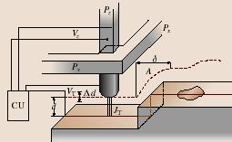
8 I 2d V exp m( V E) 0 TUNELOVÝ PRÚD ZÁVISÍ EXPONENCIÁLNE OD HRÚBKY TUNELOVEJ BARIÉRY (VZDIALENOSŤ HROTU OD POVRCHU VZORKY)!!! x z y Hrot I T V T Vzorka Schematické znázornenie posuvu hrotu nad skúmaným povrchom pomocou troch piezokryštálov. Rozmer atómu ~ m = 0.1 nm = 1 Å


9 SMER RÝCHLEHO ZÁPISU x y Rastrovanie povrchu v x-ovej a y-ovej osi. Tunelový prúd je meraný iba v smeroch vyznačených plnou čiarou. Povrch grafitu snímaný pomocou Rastrovacieho tunelového mikroskopu s atomárnym rozlišením a znázornenie jednej rastrovacej dráhy hrotu
10 Mód konštantnej výšky Mód konštantného prúdu Smer rastrovania z y Smer rastrovania x I (z=konšt.) z I=konšt. a) b) Princíp rastrovania v móde konštantného konštantnej výšky (a) a konštantného prúdu (b) V móde rastrovacieho tunelového mikroskopu iba vzorky s vodivým povrchom!!! Pozor na zmenu hustoty stavov!!!

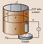
11 Typy skenerov Piezoelektrická trubica Tripod (trojnožka)
12 Rozdelenie STM podľa pracovného prostredia: 1. Vzdušný variant Pracuje na vzduchu pri teplote 300 K 2. Kryogénny variant Pracuje v kryogénnych zariadeniach, zvyčajne pri teplotách 4.2 K a nižšie s možnosťou zmeny teploty až do 300 K. 3. UHV variant Pracuje v UHV vákuovej komore pri tlaku do torr. V niektorých prípadoch je možné meniť teplotu vzorky do 76 K, resp. 4.2 K


13 Kryogénny Rastrovací silový mikroskop s antivibračným kryostatom Oxford Instruments Optistat (vľavo) a detail hlavice Rastrovacieho silového mikroskopu (vpravo) Hlavica Rastrovacieho silového mikroskopu NT MDT typ SOLVER P47 s optickým mikroskopom a CCD kamerou pre justovanie laserového lúča vzdušný variant.


14 Multifunkčné zariadenie Fy. Omicron NanoTechnology a dva typy SPM hlavíc pracujúcich pod UHV vákuom


15 Atómové rozlíšenie mica STM obrázok povrchu grafitu až po atómové rozlíšenie
16 Jednotlivé techniky na meranie a zobrazovanie povrchov
17 Základné charakteristiky jednotlivých mikroskopických metód
 N(0) E > E < j = de D( E ) de N1( E) N2( E ev ) ) 3 0 0 4π me h { f ( E) f ( E ev")
18 Meranie lokálnej hustoty stavov Hustota stavov N dn de V 2π 3 / 2 1/ 2 ( E) = = E 2 2m 2 -počet stavov na jednotkovú oblasť energie Re = E 0 E N 2 2 S(E) N(0) E > E < j = de D( E ) de N1( E) N2( E ev ) ) π me h { f ( E) f ( E ev }

19 Lokálna hustota stavov na Si


20 STM/STS MERANIE LOKÁLNEJ HUSTOTY STAVOV
21 Názov mikroskopickej metódy Name of microscopic method Akronym Engl. Typ interakcie hrotu sondy a povrchu Rastrovací tunelový mikroskop Scanning Probe Microscope Rastrovacia tunelová spektroskopia Scanning Tunneling Spectroscopy STM STS Tunelový jav Tunelový jav Atómový silový mikroskop Scanning Atomic Force Microscope Magnetický silový mikroskop Scanning Magnetic Force Microscope Elektrostatický silový mikroskop Scanning Electrostatic Force microscope Laterálny silový mikroskop Scanning Lateral Force Microscope Rastrovací teplotný mikroskop Scanning Thermal Microscopy AFM MFM EFM LFM SThM Medziatómové silové pôsobenie medzi hrotom a povrchom Pôsobenie magnetických síl medzi magnetickým hrotom sondy a magnetickým povrchom materiálu Pôsobenie elektrostatických sil medzi hrotom sondy a povrchom materiálu Ako AFM s dodatočným pôsobením aj laterálnych síl na hrot sondy Meranie teploty povrchov materiálov Rastrovací blízkopoľový optický mikroskop Scanning Near Field Optical Microscope SNOM Interakcia optického žiarenia s povrchom v submikrometrovej oblasti
 σ = 4ε r 12-6 σ r Kontaktný mód Repulzívna sila z vzdialenosť hrotu od povrchu vzorky Bezkontaktný Atraktívna sila mód Semikontaktný")
22 KRÁTKO-DOSAHOVÉ INTERAKCIE ATÓMOVÝ SILOVÝ MIKROSKOP ATOMIC FORCE MICROSCOPE - AFM Príprava hrotu Lennard-Jonesovým potenciál SILA F V( r ) σ = 4ε r 12-6 σ r Kontaktný mód Repulzívna sila z vzdialenosť hrotu od povrchu vzorky Bezkontaktný Atraktívna sila mód Semikontaktný mód
23 Metódy merania ohybu nosníka hrotu Interferometer STM Merací hrot Vzorka šošovka Kapacita Piezo - Kryštál a) b) c) Polovodičový laser Kvadrantová Dióda d) e) Niekoľko metód používaných pre meranie ohybu nosníka s hrotom a) tunelová metóda, b) interferometrická metóda, c) kapacitná metóda, d) metóda merania odrazeného lúča a e) metóda merania rozváženia Wheatstonového mostíka.


24 Princíp merania ohybu nosníka hrotu kvadrantovou diódou
 Vysokonapäťové predzosilňovače x, y, z Z z Z x x z y Z y Vzorka Kontrolná elektronika z sila")
25 Sila v smere osi z Registrácia polohy z Laterálna sila Kontrolná elektronika x, y Metóda: 1 statická 2 dynamická (oscilácia hrotu) Vysokonapäťové predzosilňovače x, y, z Z z Z x x z y Z y Vzorka Kontrolná elektronika z sila hrotu
26 Oveľa citlivejšie metódy sú založené na oscilácii držiaka hrotu a meraním zmeny jeho rezonančnej frekvencie. Tieto metódy sú založené na zmene gradientu sily F' = df/dn. Zmenou gradientu sily sa mení aj efektívna konštanta pružiny (držiaku hrotu), ktorá je daná ako c eff = c-f', kde F' je gradient sily v smere osi z, t.j.. V dôsledku zmeny konštanty pružiny sa mení aj rezonančná frekvencia systému ω 1/ 2 ' 1/ 2 ' 1/ 2 ' c = eff c F F = = ω m m c Typické závislosti amplitúdy A kmitov spružiny od frekvencie je na nasledujúcom obrázku. Amplitúda A A Bez interakcie S atraktívnou silou F Frekvencia ω Pre dve častice s priemerom 10 nm (približne priemer hrotu) a ich vzdialenosti d = 10 nm (zvyčajná vzdialenosť hrotu od povrchu ) je minimálna detekovateľná zmena sily F = 5x10-13 N a citlivosť je asi 5x10-13 m.


27 Chyby merania závislosť od tvaru ihly
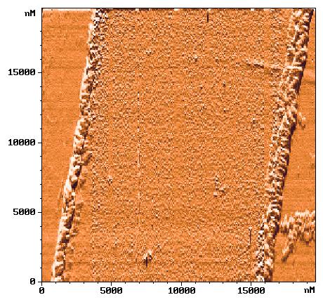
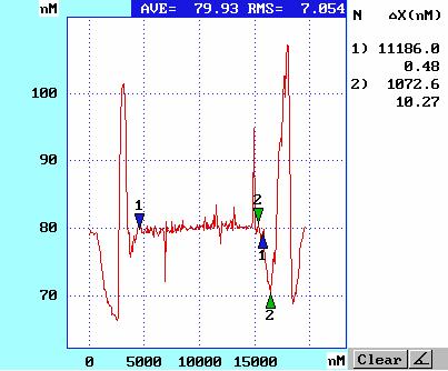
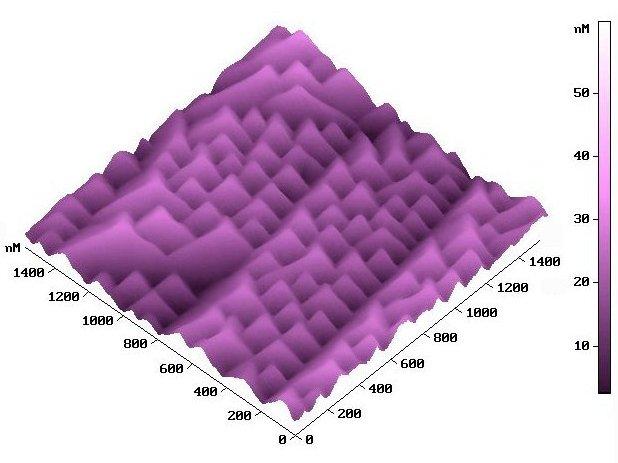
28 Topografia zafíru CdF 2 /CaF 2 epitaxná vrstva na Si


29 Nanomembrány na báze Al2O3 Polymerové fólie po protónovom ostreľovaní
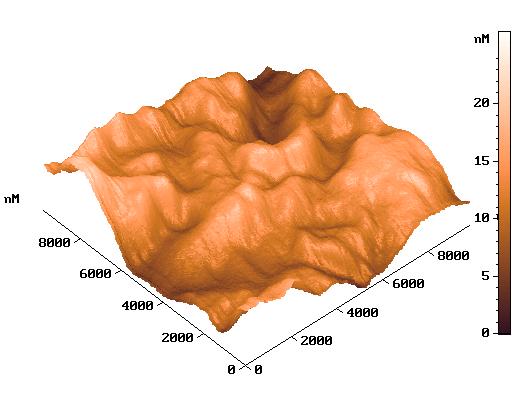
30 SPM - bio

31 Snímanie biologických objektov v imerznom prostredí pomocou AFM Červené krvinky
 aggregation of DNA molecules.")

32 All images were got in semicontact mode. a) aggregation of DNA molecules. Image was obtained in alcohol, b) vegetable ribosome-activating toxin ML1 on mica imaged in air. Single molecules are seen. 2) SPM for cells, tissues, bacteria.
33 DLHO-DOSAHOVÉ SILY Elektrostatické sily F electrostatic = ( V ) C z Magnetostatické sily F magetostatic = ( m. B ) sample Potenciál Sila Gradient sily = U = du dz 2 = d U dz 2

 42")
34 ELECTROSTATIC FORCE MICROSCOPE (VOLTAGE FORCE MICROSCOPE) Pentium IV (2000) 42 mil. tranzistorov


35 MAGNETIC FORCE MICROSCOPY Hrot pokrytý magnetickým materiálom Dráha pohybu hrotu F = m. H - nekontaktná statická metóda - nekontaktné metóda s vibráciou hrotu - s konštantnou frekvenciou - s fázovým závesom Magnetické domény meraná vzorka Hard disk Videopáska
36 THERMAL FORCE MICROSCOPE

37 FORCE MODULATION MICROSCOPE Nanoindentácia Tvrdosť Adhézia Opotrebovanie
; D.W. Pohl, W. Denk and M. Lanz, APL 44, 651 (1984)]")
38 SNOM - Scanning Near-field Optical Microscopy V roku 1870 Ernst Abbe rozlišenie dvoch objektov v optickom mikroskope: d λ 2sin Θ t.j. rozlíšenie na úrovni 200 nm SNOM rozlíšenie na úrovni 50 nm A. Lewis, M. Isaacson, A. Harootunian and A. Murray, Ultramicroscopy 13, 227 (1984); D.W. Pohl, W. Denk and M. Lanz, APL 44, 651 (1984)]


39 SNOM DNA SNOM Červená krvinka SNOM Optická mriežka
40

![FIB U 3 4 5 1 SiO 2 Si w1 w2 8 7 6 6 h ox [nm] 4 2](/docs-images/75/71561320/images/41-1.jpg "h ox [nm] 5 0 2 4 6 8 10 Voltage [V] 4 0 2 4 6 8 10")
41 AFM lokálna oxidácia AFM scratch metóda Elektrónová Si litografia + AFM Priama iónová litografia 2 - FIB U SiO 2 Si w1 w h ox [nm] 4 2 h ox [nm] Voltage [V] N


42 APPLIED PHYSICS LETTERS 91, MgB2 radio-frequency superconducting quantum interference device prepared by atomic force microscope lithography M. Gregor, T. Plecenik, M. Praščák, R. Mičunek, M. Kubinec, V.Gašparík, M. Grajcar, P. Kúš, and A. Plecenik Department of Experimental Physics, Comenius University, SK Bratislava, Slovakia
Atómová a magnetická silová mikroskopia
 Atómová a magnetická silová mikroskopia Predmet: Experimentálne metódy Bratislava, 23. októbra 2017 Milan Pavúk Ústav jadrového a fyzikálneho inžinierstva, Fakulta elektrotechniky a informatiky STU v Bratislave
Atomic and molecular interactions. Scanning probe microscopy.
 Atomic and molecular interactions. Scanning probe microscopy. Balázs Kiss Nanobiotechnology and Single Molecule Research Group, Department of Biophysics and Radiation Biology 27. November 2013. 2 Atomic
And Manipulation by Scanning Probe Microscope
 Basic 15 Nanometer Scale Measurement And Manipulation by Scanning Probe Microscope Prof. K. Fukuzawa Dept. of Micro/Nano Systems Engineering Nagoya University I. Basics of scanning probe microscope Basic
Introduction to Scanning Probe Microscopy Zhe Fei
 Introduction to Scanning Probe Microscopy Zhe Fei Phys 590B, Apr. 2019 1 Outline Part 1 SPM Overview Part 2 Scanning tunneling microscopy Part 3 Atomic force microscopy Part 4 Electric & Magnetic force
Scanning Tunneling Microscopy
 Scanning Tunneling Microscopy Scanning Direction References: Classical Tunneling Quantum Mechanics Tunneling current Tunneling current I t I t (V/d)exp(-Aφ 1/2 d) A = 1.025 (ev) -1/2 Å -1 I t = 10 pa~10na
Scanning Probe Microscopy (SPM)
") Scanning Probe Microscopy (SPM) Scanning Tunneling Microscopy (STM) --- G. Binnig, H. Rohrer et al, (1982) Near-Field Scanning Optical Microscopy (NSOM) --- D. W. Pohl (1982) Atomic Force Microscopy (AFM)
Scanning Probe Microscopy (SPM) Scanning Tunneling Microscopy (STM) --- G. Binnig, H. Rohrer et al, (1982) Near-Field Scanning Optical Microscopy (NSOM) --- D. W. Pohl (1982) Atomic Force Microscopy (AFM)
Scanning Probe Microscopy. EMSE-515 F. Ernst
 Scanning Probe Microscopy EMSE-515 F. Ernst 1 Literature 2 3 Scanning Probe Microscopy: The Lab on a Tip by Ernst Meyer,Ans Josef Hug,Roland Bennewitz 4 Scanning Probe Microscopy and Spectroscopy : Theory,
Scanning Tunneling Microscopy
 Scanning Tunneling Microscopy References: 1. G. Binnig, H. Rohrer, C. Gerber, and Weibel, Phys. Rev. Lett. 49, 57 (1982); and ibid 50, 120 (1983). 2. J. Chen, Introduction to Scanning Tunneling Microscopy,
Microscopie a stilo: principi ed esempi di applicazione
 Microscopie a stilo: principi ed esempi di applicazione Adele Sassella Dipartimento di Scienza dei Materiali Università degli Studi di Milano Bicocca adele.sassella@unimib.it Pavia, 22 aprile 2009 SCANNING
Scanning Probe Microscopy
 1 Scanning Probe Microscopy Dr. Benjamin Dwir Laboratory of Physics of Nanostructures (LPN) Benjamin.dwir@epfl.ch PH.D3.344 Outline: Introduction: What is SPM, history STM AFM Image treatment Advanced
Lecture 4 Scanning Probe Microscopy (SPM)
") Lecture 4 Scanning Probe Microscopy (SPM) General components of SPM; Tip --- the probe; Cantilever --- the indicator of the tip; Tip-sample interaction --- the feedback system; Scanner --- piezoelectric
Lecture 4 Scanning Probe Microscopy (SPM) General components of SPM; Tip --- the probe; Cantilever --- the indicator of the tip; Tip-sample interaction --- the feedback system; Scanner --- piezoelectric
Other SPM Techniques. Scanning Probe Microscopy HT10
 Other SPM Techniques Scanning Near-Field Optical Microscopy (SNOM) Scanning Capacitance Microscopy (SCM) Scanning Spreading Resistance Microscopy (SSRM) Multiprobe techniques Electrostatic Force Microscopy,
Characterization of MEMS Devices
 MEMS: Characterization Characterization of MEMS Devices Prasanna S. Gandhi Assistant Professor, Department of Mechanical Engineering, Indian Institute of Technology, Bombay, Recap Characterization of MEMS
SNOM Challenges and Solutions
 SiO x SiO x Au Au E k SNOM Challenges and Solutions Ralf Vogelgesang, Ph.D. Ralf.Vogelgesang@fkf.mpg.de Nanoscale Science Department (Prof. Kern) Max-Planck-Institut für Festkörperforschung, Stuttgart,
Module 26: Atomic Force Microscopy. Lecture 40: Atomic Force Microscopy 3: Additional Modes of AFM
 Module 26: Atomic Force Microscopy Lecture 40: Atomic Force Microscopy 3: Additional Modes of AFM 1 The AFM apart from generating the information about the topography of the sample features can be used
Scanning Probe Microscopy: Atomic Force Microscopy And Scanning Tunneling Microscopy (NanoScience And Technology) [Kindle Edition] By Bert Voigtl
![Scanning Probe Microscopy: Atomic Force Microscopy And Scanning Tunneling Microscopy (NanoScience And Technology) [Kindle Edition] By Bert Voigtl](/thumbs/81/83165600.jpg "Scanning Probe Microscopy: Atomic Force Microscopy And Scanning Tunneling Microscopy (NanoScience And Technology) [Kindle Edition] By Bert Voigtl") Scanning Probe Microscopy: Atomic Force Microscopy And Scanning Tunneling Microscopy (NanoScience And Technology) [Kindle Edition] By Bert Voigtl READ ONLINE If searched for a book Scanning Probe Microscopy:
Scanning Probe Microscopy: Atomic Force Microscopy And Scanning Tunneling Microscopy (NanoScience And Technology) [Kindle Edition] By Bert Voigtl READ ONLINE If searched for a book Scanning Probe Microscopy:
(Scanning Probe Microscopy)
") (Scanning Probe Microscopy) Ing-Shouh Hwang (ishwang@phys.sinica.edu.tw) Institute of Physics, Academia Sinica, Taipei, Taiwan References 1. G. Binnig, H. Rohrer, C. Gerber, and Weibel, Phys. Rev. Lett.
(Scanning Probe Microscopy) Ing-Shouh Hwang (ishwang@phys.sinica.edu.tw) Institute of Physics, Academia Sinica, Taipei, Taiwan References 1. G. Binnig, H. Rohrer, C. Gerber, and Weibel, Phys. Rev. Lett.
Control of Dynamics of SPM Probes for Non-destructive Defectoscopy
 XXX. ASR '2005 Seminar, Instruments and Control, Ostrava, April 29, 2005 209 Control of Dynamics of SPM Probes for Non-destructive Defectoscopy KALA, Jaroslav Ing., Physics Department, FEEC, BUT, Technická
Surface Studies by Scanning Tunneling Microscopy
 Surface Studies by Scanning Tunneling Microscopy G. Binnig, H. Rohrer, Ch. Gerber, and E. Weibel IBM Zurich Research Laboratory, 8803 Ruschlikon-ZH, Switzerland (Received by Phys. Rev. Lett. on 30th April,
Low Temperature Physics Measurement Systems
 PAGE 6 & 2008 2007 PRODUCT CATALOG Accelerate your Semiconductor Research & Developments towards Nanoscale Products. Experience your new working horse in the emerging field of semiconductor research for
Scanning Probe Microscopy (SPM)
") CHEM53200: Lecture 9 Scanning Probe Microscopy (SPM) Major reference: 1. Scanning Probe Microscopy and Spectroscopy Edited by D. Bonnell (2001). 2. A practical guide to scanning probe microscopy by Park
CHEM53200: Lecture 9 Scanning Probe Microscopy (SPM) Major reference: 1. Scanning Probe Microscopy and Spectroscopy Edited by D. Bonnell (2001). 2. A practical guide to scanning probe microscopy by Park
STM: Scanning Tunneling Microscope
 STM: Scanning Tunneling Microscope Basic idea STM working principle Schematic representation of the sample-tip tunnel barrier Assume tip and sample described by two infinite plate electrodes Φ t +Φ s =
Optics and Spectroscopy
 Introduction to Optics and Spectroscopy beyond the diffraction limit Chi Chen 陳祺 Research Center for Applied Science, Academia Sinica 2015Apr09 1 Light and Optics 2 Light as Wave Application 3 Electromagnetic
Scanning Probe Microscopy. Amanda MacMillan, Emmy Gebremichael, & John Shamblin Chem 243: Instrumental Analysis Dr. Robert Corn March 10, 2010
 Scanning Probe Microscopy Amanda MacMillan, Emmy Gebremichael, & John Shamblin Chem 243: Instrumental Analysis Dr. Robert Corn March 10, 2010 Scanning Probe Microscopy High-Resolution Surface Analysis
MRSEC. Refrigerator Magnet Activity Guide. Quick Reference Activity Guide. a) b) c) = north = south. Activity Materials
 b) c) = north = south. Activity Materials") MRSEC Refrigerator Magnet Activity Guide Quick Reference Activity Guide Activity Materials Refrigerator magnet with removable probe strip Magnetic field diagrams Starting Points One of the great breakthroughs
MRSEC Refrigerator Magnet Activity Guide Quick Reference Activity Guide Activity Materials Refrigerator magnet with removable probe strip Magnetic field diagrams Starting Points One of the great breakthroughs
672 Advanced Solid State Physics. Scanning Tunneling Microscopy
 672 Advanced Solid State Physics Scanning Tunneling Microscopy Biao Hu Outline: 1. Introduction to STM 2. STM principle & working modes 3. STM application & extension 4. STM in our group 1. Introduction
Experimental methods in physics. Local probe microscopies I
 Experimental methods in physics Local probe microscopies I Scanning tunnelling microscopy (STM) Jean-Marc Bonard Academic year 09-10 1. Scanning Tunneling Microscopy 1.1. Introduction Image of surface
PY5020 Nanoscience Scanning probe microscopy
 PY500 Nanoscience Scanning probe microscopy Outline Scanning tunnelling microscopy (STM) - Quantum tunnelling - STM tool - Main modes of STM Contact probes V bias Use the point probes to measure the local
Chapter 5 Nanomanipulation. Chapter 5 Nanomanipulation. 5.1: With a nanotube. Cutting a nanotube. Moving a nanotube
 Objective: learn about nano-manipulation techniques with a STM or an AFM. 5.1: With a nanotube Moving a nanotube Cutting a nanotube Images at large distance At small distance : push the NT Voltage pulse
tip of a current tip and the sample. Components: 3. Coarse sample-to-tip isolation system, and
 SCANNING TUNNELING MICROSCOPE Brief history: Heinrich Rohrer and Gerd K. Binnig, scientists at IBM's Zurich Research Laboratory in Switzerland, are awarded the 1986 Nobel Prize in physicss for their work
Scanning Probe Microscopy (SPM)
") http://ww2.sljus.lu.se/staff/rainer/spm.htm Scanning Probe Microscopy (FYST42 / FAFN30) Scanning Probe Microscopy (SPM) overview & general principles March 23 th, 2018 Jan Knudsen, room K522, jan.knudsen@sljus.lu.se
http://ww2.sljus.lu.se/staff/rainer/spm.htm Scanning Probe Microscopy (FYST42 / FAFN30) Scanning Probe Microscopy (SPM) overview & general principles March 23 th, 2018 Jan Knudsen, room K522, jan.knudsen@sljus.lu.se
AFM for Measuring Surface Topography and Forces
 ENB 2007 07.03.2007 AFM for Measuring Surface Topography and Forces Andreas Fery Scanning Probe : What is it and why do we need it? AFM as a versatile tool for local analysis and manipulation Dates Course
Reducing dimension. Crystalline structures
 Reducing dimension 2D surfaces, interfaces and quantum wells 1D carbon nanotubes, quantum wires and conducting polymers 0D nanocrystals, nanoparticles, lithographically patterned quantum dots Crystalline
Program Operacyjny Kapitał Ludzki SCANNING PROBE TECHNIQUES - INTRODUCTION
 Program Operacyjny Kapitał Ludzki SCANNING PROBE TECHNIQUES - INTRODUCTION Peter Liljeroth Department of Applied Physics, Aalto University School of Science peter.liljeroth@aalto.fi Projekt współfinansowany
Today s SPM in Nanotechnology
 Today s SPM in Nanotechnology An introduction for Advanced Applications Qun (Allen) Gu, Ph.D., AFM Scientist, Pacific Nanotechnology IEEE Bay Area Nanotechnology Council, August, 2007 8/17/2015 1 Content
Contents. What is AFM? History Basic principles and devices Operating modes Application areas Advantages and disadvantages
 Contents What is AFM? History Basic principles and devices Operating modes Application areas Advantages and disadvantages Figure1: 2004 Seth Copen Goldstein What is AFM? A type of Scanning Probe Microscopy
Physics Faculty Publications and Presentations
 Portland State University PDXScholar Physics Faculty Publications and Presentations Physics 9-2-2010 Systems for Assessing and Enhancing the Performance of Scanning Electron Microscopes by Quantifying
Chapter 10. Nanometrology. Oxford University Press All rights reserved.
 Chapter 10 Nanometrology Oxford University Press 2013. All rights reserved. 1 Introduction Nanometrology is the science of measurement at the nanoscale level. Figure illustrates where nanoscale stands
Understanding the properties and behavior of groups of interacting atoms more than simple molecules
 Condensed Matter Physics Scratching the Surface Understanding the properties and behavior of groups of interacting atoms more than simple molecules Solids and fluids in ordinary and exotic states low energy
Scanning Tunneling Microscopy
 Scanning Tunneling Microscopy References: 1. G. Binnig, H. Rohrer, C. Gerber, and Weibel, Phys. Rev. Lett. 49, 57 (1982); and ibid 50, 120 (1983). 2. J. Chen, Introduction to Scanning Tunneling Microscopy,
Chapter 9. Electron mean free path Microscopy principles of SEM, TEM, LEEM
 Chapter 9 Electron mean free path Microscopy principles of SEM, TEM, LEEM 9.1 Electron Mean Free Path 9. Scanning Electron Microscopy (SEM) -SEM design; Secondary electron imaging; Backscattered electron
Nanostructure. Materials Growth Characterization Fabrication. More see Waser, chapter 2
 Nanostructure Materials Growth Characterization Fabrication More see Waser, chapter 2 Materials growth - deposition deposition gas solid Physical Vapor Deposition Chemical Vapor Deposition Physical Vapor
SCANNING-PROBE TECHNIQUES OR APPARATUS; APPLICATIONS OF SCANNING-PROBE TECHNIQUES, e.g. SCANNING PROBE MICROSCOPY [SPM]
![SCANNING-PROBE TECHNIQUES OR APPARATUS; APPLICATIONS OF SCANNING-PROBE TECHNIQUES, e.g. SCANNING PROBE MICROSCOPY [SPM]](/thumbs/81/83165631.jpg "SCANNING-PROBE TECHNIQUES OR APPARATUS; APPLICATIONS OF SCANNING-PROBE TECHNIQUES, e.g. SCANNING PROBE MICROSCOPY [SPM]") G01Q SCANNING-PROBE TECHNIQUES OR APPARATUS; APPLICATIONS OF SCANNING-PROBE TECHNIQUES, e.g. SCANNING PROBE MICROSCOPY [SPM] Scanning probes, i.e. devices having at least a tip of nanometre sized dimensions
G01Q SCANNING-PROBE TECHNIQUES OR APPARATUS; APPLICATIONS OF SCANNING-PROBE TECHNIQUES, e.g. SCANNING PROBE MICROSCOPY [SPM] Scanning probes, i.e. devices having at least a tip of nanometre sized dimensions
Od zmiešavacieho kalorimetra k ultra citlivej modulovanej kalorimetrii. Jozef Kačmarčík
 Od zmiešavacieho kalorimetra k ultra citlivej modulovanej kalorimetrii CENTRUM FYZIKY VEĽMI NÍZKYCH TEPLÔT Ústavu experimentálnej fyziky SAV a Univerzity P.J.Šafárika Centrum excelentnosti SAV Jozef Kačmarčík
CHARACTERIZATION of NANOMATERIALS KHP
 CHARACTERIZATION of NANOMATERIALS Overview of the most common nanocharacterization techniques MAIN CHARACTERIZATION TECHNIQUES: 1.Transmission Electron Microscope (TEM) 2. Scanning Electron Microscope
Single-Molecule Recognition and Manipulation Studied by Scanning Probe Microscopy
 Single-Molecule Recognition and Manipulation Studied by Scanning Probe Microscopy Byung Kim Department of Physics Boise State University Langmuir (in press, 2006) swollen collapsed Hydrophilic non-sticky
Fyzika kondenzovaných látok
 Fyzika kondenzovaných látok Štúdium dynamických magnetických vlastností a relaxačných procesov v magnetických nanočasticiach. školiteľ: doc. RNDr. Adriana Zeleňáková, PhD. Anotácia: Mono-doménové magnetické
Crystalline Surfaces for Laser Metrology
 Crystalline Surfaces for Laser Metrology A.V. Latyshev, Institute of Semiconductor Physics SB RAS, Novosibirsk, Russia Abstract: The number of methodological recommendations has been pronounced to describe
Magnetic Resonance Force Microscopy. Christian Degen Department of Physics, ETH Zurich, Switzerland
 Magnetic Resonance Force Microscopy Christian Degen Department of Physics, ETH Zurich, Switzerland CIMST Summer School 2014 From Andreas Trabesinger / Wikipedia Scale of things 1m 1mm 1µm 1-100 nm 1nm
Bridge between research in modern physics and entrepreneurship in nanotechnology. Quantum Physics
 Bridge between research in modern physics and entrepreneurship in nanotechnology Quantum Physics The physics of the very small with great applications Part 2 QUANTUM PROPERTIES & TECHNOLOGY TRANSLATION
MS482 Materials Characterization ( 재료분석 ) Lecture Note 11: Scanning Probe Microscopy. Byungha Shin Dept. of MSE, KAIST
 Lecture Note 11: Scanning Probe Microscopy. Byungha Shin Dept. of MSE, KAIST") 2015 Fall Semester MS482 Materials Characterization ( 재료분석 ) Lecture Note 11: Scanning Probe Microscopy Byungha Shin Dept. of MSE, KAIST 1 Course Information Syllabus 1. Overview of various characterization
2015 Fall Semester MS482 Materials Characterization ( 재료분석 ) Lecture Note 11: Scanning Probe Microscopy Byungha Shin Dept. of MSE, KAIST 1 Course Information Syllabus 1. Overview of various characterization
Scanning Tunneling Microscopy
 Scanning Tunneling Microscopy A scanning tunneling microscope (STM) is an instrument for imaging surfaces at the atomic level. Its development in 1981 earned its inventors, Gerd Binnig and Heinrich Rohrer
Basic Laboratory. Materials Science and Engineering. Atomic Force Microscopy (AFM)
") Basic Laboratory Materials Science and Engineering Atomic Force Microscopy (AFM) M108 Stand: 20.10.2015 Aim: Presentation of an application of the AFM for studying surface morphology. Inhalt 1.Introduction...
Basic Laboratory Materials Science and Engineering Atomic Force Microscopy (AFM) M108 Stand: 20.10.2015 Aim: Presentation of an application of the AFM for studying surface morphology. Inhalt 1.Introduction...
Iodine-Mediated Chemical Vapor Deposition Growth of Metastable Transition Metal
 Supporting Information Iodine-Mediated Chemical Vapor Deposition Growth of Metastable Transition Metal Dichalcogenides Qiqi Zhang,, Yao Xiao, #, Tao Zhang,, Zheng Weng, Mengqi Zeng, Shuanglin Yue, ± Rafael
Carbon Nanomaterials
 Carbon Nanomaterials STM Image 7 nm AFM Image Fullerenes C 60 was established by mass spectrographic analysis by Kroto and Smalley in 1985 C 60 is called a buckminsterfullerene or buckyball due to resemblance
Atomic Force Microscopy (AFM) Part I
 Part I") Atomic Force Microscopy (AFM) Part I CHEM-L2000 Eero Kontturi 6 th March 2018 Lectures on AFM Part I Principles and practice Imaging of native materials, including nanocellulose Part II Surface force measurements
Atomic Force Microscopy (AFM) Part I CHEM-L2000 Eero Kontturi 6 th March 2018 Lectures on AFM Part I Principles and practice Imaging of native materials, including nanocellulose Part II Surface force measurements
Probing Molecular Electronics with Scanning Probe Microscopy
 Probing Molecular Electronics with Scanning Probe Microscopy Mark C. Hersam Assistant Professor Department of Materials Science and Engineering, Northwestern University, Evanston, IL 60208-3108 Ph: 847-491-2696,
Scanning Tunneling Microscopy/Spectroscopy
 Scanning Tunneling Microscopy/Spectroscopy 0 Scanning Tunneling Microscope 1 Scanning Tunneling Microscope 2 Scanning Tunneling Microscope 3 Typical STM talk or paper... The differential conductance di/dv
From nanophysics research labs to cell phones. Dr. András Halbritter Department of Physics associate professor
 From nanophysics research labs to cell phones Dr. András Halbritter Department of Physics associate professor Curriculum Vitae Birth: 1976. High-school graduation: 1994. Master degree: 1999. PhD: 2003.
General concept and defining characteristics of AFM. Dina Kudasheva Advisor: Prof. Mary K. Cowman
 General concept and defining characteristics of AFM Dina Kudasheva Advisor: Prof. Mary K. Cowman Overview Introduction History of the SPM invention Technical Capabilities Principles of operation Examples
bio-molecular studies Physical methods in Semmelweis University Osváth Szabolcs
 Physical methods in bio-molecular studies Osváth Szabolcs Semmelweis University szabolcs.osvath@eok.sote.hu Light emission and absorption spectra Stokes shift is the difference (in wavelength or frequency
Molecular and carbon based electronic systems
 Molecular and carbon based electronic systems Single molecule deposition and properties on surfaces Bottom Up Top Down Fundamental Knowledge & Functional Devices Thilo Glatzel, thilo.glatzel@unibas.ch
Introduction to Scanning Probe Microscopy
 WORKSHOP Nanoscience on the Tip Introduction to Scanning Probe Microscopy Table of Contents: 1 Historic Perspectives... 1 2 Scanning Force Microscopy (SFM)... 2 2.1. Contact Mode... 2 2.2. AC Mode Imaging...
Intermittent-Contact Mode Force Microscopy & Electrostatic Force Microscopy (EFM)
") WORKSHOP Nanoscience on the Tip Intermittent-Contact Mode Force Microscopy & Electrostatic Force Microscopy (EFM) Table of Contents: 1. Motivation... 1. Simple Harmonic Motion... 1 3. AC-Mode Imaging...
WORKSHOP Nanoscience on the Tip Intermittent-Contact Mode Force Microscopy & Electrostatic Force Microscopy (EFM) Table of Contents: 1. Motivation... 1. Simple Harmonic Motion... 1 3. AC-Mode Imaging...
AFM: Atomic Force Microscopy II
 AM: Atomic orce Microscopy II Jan Knudsen The MAX IV laboratory & Division of synchrotron radiation research K522-523 (Sljus) 4 th of May, 2018 http://www.sljus.lu.se/staff/rainer/spm.htm Last time: The
Nanoelectronics 09. Atsufumi Hirohata Department of Electronics. Quick Review over the Last Lecture
 Nanoelectronics 09 Atsufumi Hirohata Department of Electronics 13:00 Monday, 12/February/2018 (P/T 006) Quick Review over the Last Lecture ( Field effect transistor (FET) ): ( Drain ) current increases
MSE 321 Structural Characterization
 Auger Spectroscopy Auger Electron Spectroscopy (AES) Scanning Auger Microscopy (SAM) Incident Electron Ejected Electron Auger Electron Initial State Intermediate State Final State Physical Electronics
CH676 Physical Chemistry: Principles and Applications. CH676 Physical Chemistry: Principles and Applications
 CH676 Physical Chemistry: Principles and Applications History of Nanotechnology: Time Line Democritus in ancient Greece: concept of atom 1900 : Rutherford : discovery of atomic nucleus The first TEM was
Ecole Franco-Roumaine : Magnétisme des systèmes nanoscopiques et structures hybrides - Brasov, Modern Analytical Microscopic Tools
 1. Introduction Solid Surfaces Analysis Group, Institute of Physics, Chemnitz University of Technology, Germany 2. Limitations of Conventional Optical Microscopy 3. Electron Microscopies Transmission Electron
Scanning Gate Microscopy (SGM) of semiconductor nanostructures
 of semiconductor nanostructures") Scanning Gate Microscopy (SGM) of semiconductor nanostructures H. Sellier, P. Liu, B. Sacépé, S. Huant Dépt NANO, Institut NEEL, Grenoble, France B. Hackens, F. Martins, V. Bayot UCL, Louvain-la-Neuve,
Scanning Gate Microscopy (SGM) of semiconductor nanostructures H. Sellier, P. Liu, B. Sacépé, S. Huant Dépt NANO, Institut NEEL, Grenoble, France B. Hackens, F. Martins, V. Bayot UCL, Louvain-la-Neuve,
Surface Characte i r i zat on LEED Photoemission Phot Linear optics
 Surface Characterization i LEED Photoemission Linear optics Surface characterization with electrons MPS M.P. Seah, WA W.A. Dench, Surf. Interf. Anal. 1 (1979) 2 LEED low energy electron diffraction De
AFM (Atomic force microscope) a jeho využitie pri štúdiu povrchu a povrchových síl minerálov
 a jeho využitie pri štúdiu povrchu a povrchových síl minerálov") AFM (Atomic force microscope) a jeho využitie pri štúdiu povrchu a povrchových síl minerálov Jiří Škvarla 1 AFM (Atomic force microscope) and its use in studying the surface and surface forces of minerals
AFM (Atomic force microscope) a jeho využitie pri štúdiu povrchu a povrchových síl minerálov Jiří Škvarla 1 AFM (Atomic force microscope) and its use in studying the surface and surface forces of minerals
Lecture 12. study surfaces.
 Lecture 12 Solid Surfaces Techniques to Solid Surfaces. Techniques to study surfaces. Solid Surfaces Molecules on surfaces are not mobile (to large extent) Surfaces have a long-range order (crystalline)
Santosh Devasia Mechanical Eng. Dept., UW
 Nano-positioning Santosh Devasia Mechanical Eng. Dept., UW http://faculty.washington.edu/devasia/ Outline of Talk 1. Why Nano-positioning 2. Sensors for Nano-positioning 3. Actuators for Nano-positioning
Scanning Force Microscopy And Related Techniques. With the help of.
 With the help of. 1. Yosi Shacham TAU 2. Yossi Rosenwacks TAU 3. Julio Gomez-Herrero UAM 4. Adriana Gil - UAM 5. Serge Lemay - Delft 6. Hezy Cohen - HUJI 7. Scanning Force Microscopy And Related Techniques
chiral m = n Armchair m = 0 or n = 0 Zigzag m n Chiral Three major categories of nanotube structures can be identified based on the values of m and n
 zigzag armchair Three major categories of nanotube structures can be identified based on the values of m and n m = n Armchair m = 0 or n = 0 Zigzag m n Chiral Nature 391, 59, (1998) chiral J. Tersoff,
Fabrication / Synthesis Techniques
 Quantum Dots Physical properties Fabrication / Synthesis Techniques Applications Handbook of Nanoscience, Engineering, and Technology Ch.13.3 L. Kouwenhoven and C. Marcus, Physics World, June 1998, p.35
Scanning tunneling microscopy of monoatomic gold chains on vicinal Si(335) surface: experimental and theoretical study
 surface: experimental and theoretical study") phys. stat. sol. (b) 4, No., 33 336 (005) / DOI 10.100/pssb.00460056 Scanning tunneling microscopy of monoatomic gold chains on vicinal Si(335) surface: experimental and theoretical study M. Krawiec *,
phys. stat. sol. (b) 4, No., 33 336 (005) / DOI 10.100/pssb.00460056 Scanning tunneling microscopy of monoatomic gold chains on vicinal Si(335) surface: experimental and theoretical study M. Krawiec *,
Combining High Resolution Optical and Scanning Probe Microscopy
 Combining High Resolution Optical and Scanning Probe Microscopy Fernando Vargas WITec, Ulm, Germany www.witec.de Company Background Foundation 1997 by O. Hollricher, J. Koenen, K. Weishaupt WITec = Wissenschaftliche
Lecture 26 MNS 102: Techniques for Materials and Nano Sciences
 Lecture 26 MNS 102: Techniques for Materials and Nano Sciences Reference: #1 C. R. Brundle, C. A. Evans, S. Wilson, "Encyclopedia of Materials Characterization", Butterworth-Heinemann, Toronto (1992),
AP5301/ Name the major parts of an optical microscope and state their functions.
 Review Problems on Optical Microscopy AP5301/8301-2015 1. Name the major parts of an optical microscope and state their functions. 2. Compare the focal lengths of two glass converging lenses, one with
MSE 321 Structural Characterization
 Auger Spectroscopy Auger Electron Spectroscopy (AES) Scanning Auger Microscopy (SAM) Incident Electron Ejected Electron Auger Electron Initial State Intermediate State Final State Physical Electronics
Clark Atlanta University Center for Surface Chemistry and Catalysis Instrument Capabilities
 Center for Surface Chemistry and Catalysis Instrument Capabilities For information contact: Dr. Eric Mintz Research Center for Science and Technology Clark Atlanta University Atlanta, Georgia 30314 Phone:
Application of electrostatic force microscopy in nanosystem diagnostics
 Materials Science, Vol., No. 3, 003 Application of electrostatic force microscopy in nanosystem diagnostics TEODOR P. GOTSZALK *, PIOTR GRABIEC, IVO W. RANGELOW 3 Fulty of Microsystem Electronics and Photonics,
Atomic Scale Coupling of Electromagnetic Radiation to Single Molecules. Wilson Ho University of California, Irvine
 Atomic Scale Coupling of Electromagnetic Radiation to Single Molecules Wilson Ho University of California, Irvine Surface Photochemistry Direct Adsorbate Excitation Photoelectron Mechanism Objective How
STM spectroscopy (STS)
") STM spectroscopy (STS) di dv 4 e ( E ev, r) ( E ) M S F T F Basic concepts of STS. With the feedback circuit open the variation of the tunneling current due to the application of a small oscillating voltage
STM spectroscopy (STS) di dv 4 e ( E ev, r) ( E ) M S F T F Basic concepts of STS. With the feedback circuit open the variation of the tunneling current due to the application of a small oscillating voltage
Nanotechnology. Gavin Lawes Department of Physics and Astronomy
 Nanotechnology Gavin Lawes Department of Physics and Astronomy Earth-Moon distance 4x10 8 m (courtesy NASA) Length scales (Part I) Person 2m Magnetic nanoparticle 5x10⁻⁹ m 10 10 m 10 5 m 1 m 10-5 m 10-10
INTRODUCTION TO SCA\ \I\G TUNNELING MICROSCOPY
 INTRODUCTION TO SCA\ \I\G TUNNELING MICROSCOPY SECOND EDITION C. JULIAN CHEN Department of Applied Physics and Applied Mathematics, Columbia University, New York OXFORD UNIVERSITY PRESS Contents Preface
NIS: what can it be used for?
 AFM @ NIS: what can it be used for? Chiara Manfredotti 011 670 8382/8388/7879 chiara.manfredotti@to.infn.it Skype: khiaram 1 AFM: block scheme In an Atomic Force Microscope (AFM) a micrometric tip attached
Scanning Tunneling Microscopy
 Scanning Tunneling Microscopy References: 1. G. Binnig, H. Rohrer, C. Gerber, and Weibel, Phys. Rev. Lett. 49, 57 (1982); and ibid 50, 120 (1983). 2. J. Chen, Introduction to Scanning Tunneling Microscopy,
From manipulation of the charge state to imaging of individual molecular orbitals and bond formation
 Scanning Probe Microscopy of Adsorbates on Insulating Films: From manipulation of the charge state to imaging of individual molecular orbitals and bond formation Gerhard Meyer, Jascha Repp, Peter Liljeroth
2D Materials Research Activities at the NEST lab in Pisa, Italy. Stefan Heun NEST, Istituto Nanoscienze-CNR and Scuola Normale Superiore, Pisa, Italy
 2D Materials Research Activities at the NEST lab in Pisa, Italy Stefan Heun NEST, Istituto Nanoscienze-CNR and Scuola Normale Superiore, Pisa, Italy 2D Materials Research Activities at the NEST lab in
MAGNETIC FORCE MICROSCOPY
 University of Ljubljana Faculty of Mathematics and Physics Department of Physics SEMINAR MAGNETIC FORCE MICROSCOPY Author: Blaž Zupančič Supervisor: dr. Igor Muševič February 2003 Contents 1 Abstract 3
Instrumentation and Operation
 Instrumentation and Operation 1 STM Instrumentation COMPONENTS sharp metal tip scanning system and control electronics feedback electronics (keeps tunneling current constant) image processing system data
Integrating MEMS Electro-Static Driven Micro-Probe and Laser Doppler Vibrometer for Non-Contact Vibration Mode SPM System Design
 Tamkang Journal of Science and Engineering, Vol. 12, No. 4, pp. 399 407 (2009) 399 Integrating MEMS Electro-Static Driven Micro-Probe and Laser Doppler Vibrometer for Non-Contact Vibration Mode SPM System
Scanning Probe Microscopies (SPM)
") Scanning Probe Microscopies (SPM) Nanoscale resolution af objects at solid surfaces can be reached with scanning probe microscopes. They allow to record an image of the surface atomic arrangement in direct
Scanning Probe Microscopies (SPM) Nanoscale resolution af objects at solid surfaces can be reached with scanning probe microscopes. They allow to record an image of the surface atomic arrangement in direct
Electronic transport in low dimensional systems
 Electronic transport in low dimensional systems For example: 2D system l
Spectroscopy at nanometer scale
 Spectroscopy at nanometer scale 1. Physics of the spectroscopies 2. Spectroscopies for the bulk materials 3. Experimental setups for the spectroscopies 4. Physics and Chemistry of nanomaterials Various
Microscopical and Microanalytical Methods (NANO3)
") Microscopical and Microanalytical Methods (NANO3) 06.11.15 10:15-12:00 Introduction - SPM methods 13.11.15 10:15-12:00 STM 20.11.15 10:15-12:00 STS Erik Zupanič erik.zupanic@ijs.si stm.ijs.si 27.11.15
Microscopical and Microanalytical Methods (NANO3) 06.11.15 10:15-12:00 Introduction - SPM methods 13.11.15 10:15-12:00 STM 20.11.15 10:15-12:00 STS Erik Zupanič erik.zupanic@ijs.si stm.ijs.si 27.11.15
CNPEM Laboratório de Ciência de Superfícies
 Investigating electrical charged samples by scanning probe microscopy: the influence to magnetic force microscopy and atomic force microscopy phase images. Carlos A. R. Costa, 1 Evandro M. Lanzoni, 1 Maria