Lecture: Solid State Chemistry (Festkörperchemie) Part 1. H.J. Deiseroth, SS 2006
|
|
|
- Terence Walker
- 6 years ago
- Views:
Transcription
1 Lecture: Solid State Chemistry (Festkörperchemie) Part 1 H.J. Deiseroth, SS 2006

2 Resources
 W.H.")
 recommendation german very good,")


 IUCR-teaching")
3 Resources Textbooks: Shriver, Atkins, Inorganic Chemistry (3rd ed, 1999) W.H. Freeman and Company (Chapter 2, 18...) recommendation german very good, but not basic level Internet resources (german) (pdf-downloads) IUCR-teaching resources (International Union for Crystallography, advanced level)


4 Resources Journals
5 Lattice Energy and Chemical Bonding in Solids
6 Lattice enthalpy H 0 L The lattice enthalpy change is the standard molar enthalpy change for the following process: M + (gas) + X - (gas) MX (solid) H 0 L Because the formation of a solid from a gas of ions is always exothermic lattice enthalpies (defined in this way!!) are usually negative numbers. If entropy considerations are neglected the most stable crystal structure of a given compound is the one with the highest lattice enthalpy.
7 Lattice enthalpies can be determined by a thermodynamic cycle Born-Haber cycle A Born-Haber cycle for KCl (all enthalpies: kj mol -1 for normal conditions standard enthalpies) delete standard enthalpies of - sublimation: +89 (K) - ionization: (K) - atomization: +244 (Cl 2 ) - electron affinity: -355 (Cl) - lattice enthalpy: x
8 Calculation of lattice enthalpies Η 0 L = V + V AB Born V AB = Coulomb (electrostatic) interaction between all cations and anions treated as point charges (Madelung part of lattice enthalpy ( MAPLE ) V Born = Repulsion due to overlap of electron clouds (Born repulsion)
9 Calculation of lattice enthalpies 1. MAPLE (V AB ) (Coulombic contributions to lattice enthalpies, MADELUNG part of lattice enthalpy, atoms treated as point charges ) V AB = A z + 4πε z 0 r e 2 AB N Coulomb potential of an ion pair V AB : Coulomb potential (electrostatic potential) A: Madelung constant (depends on structure type) N: Avogadro constant z: charge number e: elementary charge ε o : dielectric constant (vacuum permittivity) r AB : shortest distance between cation and anion
 ZnS: 1.638 (sphalerite) ion pair: 1.0000 (!) A = 12 8 6 6 + + 2 3 2 24 5... = 1.748... (NaCl) (infinite summation)")
10 Calculation of the Madelung constant Cl Na typical for 3D ionic solids: Coulomb attraction and repulsion Madelung constants: CsCl: NaCl: ZnS: (wurtzite) ZnS: (sphalerite) ion pair: (!) A = = (NaCl) (infinite summation)
11 2. Born repulsion (V Born ) (Repulsion arising from overlap of electron clouds, atoms do not behave as point charges) V AB r 0 Because the electron density of atoms decreases exponentially towards zero at large distances from the nucleus the Born repulsion shows the same behaviour r approximation: V Born = B r n V AB B and n are constants for a given atom type; n can be derived from compressibility measurements (~8)
12 Total lattice enthalpy from Coulomb interaction and Born repulsion 0 ΗL = Min.( V + V Η 0 L = A AB 2 z+ z e 4πε 0r0 N (1 Born (set first derivative of the sum to zero) 1 ) n Calculated lattice enthalpies (kj mol -1 ): NaCl ( 772), CsCl (-653) From Born Haber cycle: NaCl (-757), CsCl (-623) (based on the known enthalpy of formation!!) Applications of lattice enthalpy calculations: lattice enthalpies and stabilities of non existent compounds and calculations of electron affinity data (see next transparencies) Solubility of salts in water (see Shriver-Atkins) )
13 Calculation of the lattice enthalpy for NaCl Η 0 L = A 2 z+ z e 4πε 0r0 N (1 1 ) n ε 0 = As/Vm; e = As (=C); N = mol -1 A = 1.746; r = m; n = 8 (Born exponent) 1/4πε 0 = e 2 N = (only for univalent ions!) H L = A/r 0 (1-1/n) (only for univalent ions!) Vm A 2 s 2 VAs Dimensions: = = J/mol As m mol -1 mol NaCl: H L = kj mol -1 (only MAPLE) H L = kj mol -1 (including Born repulsion)
14 Can MgCl (Mg + Cl - ) crystallizing in the rocksalt structure be a stable solid? H Formation ~ -126 kj mol -1 (calculated from Born Haber cycle based on similar r AB as for NaCl!!) MgCl should be a stable compound!!!!! However: Chemical intuition should warn you that there is a risk of disproportionation: 2 MgCl 2(s) Mg (s) + MgCl 2(s) H Disprop =???????? MgCl 2 Mg + Cl 2 H F = +252 kj (twice the enthalpy of formation) Mg + Cl 2 MgCl 2 H F = -640 kj (from calorimetric measurement) Σ 2 MgCl Mg + MgCl 2 H Dispr = -388 kj (Disproportionation reaction is favored)
15 Calculation of the electron affinity for Cl from the Born-Haber cycle for CsCl Standard enthalpy of formation kj/mol sublimation 70.3 ½ atomization ionization Lattice enthalpy H Formation = H subl + ½ H Diss + H Ion + H EA + H Lattice H EA = H F (H S + ½ H D + H I + H L ) H EA = ( ) =
16 Chemical bonding in solids bonding theory of solids must account for their basic properties as: - mechanism and temperature dependence of the electrical conductivity of isolators, semiconductors, metals and alloys (further important properties: luster of metals, thermal conductivity and color of solids, ductility and malleability of metals)...
17 Temperature dependence of the electrical conductivity (σ) and resistivity (R) of metals semiconductors, isolators, superconductors high concentration of charge carriers (electrons) = alloy increasing resistivity with temperature (due to increased scattering of charge carriers) resistivity below T c is zero!! (special mechanism of conductivity) low concentration of charge carriers (electrons) = isolator decreasing resistivity with temperature (due to increasing thermal excitation of electrons) key to understanding: band model
 the overlap of atomic")
 δe << kt ~ 0.")
18 The origin of the simple band model for solids: Band formation by orbital overlap (in principle a continuation of the Molecular Orbital model) the overlap of atomic orbitals in a solid gives rise to the formation of bands separated by gaps (the band width is a rough measure of interaction between neighbouring atoms) δe << kt ~ ev


19 s- and p-bands in a one-dimensional solid Energy s-band p-band

20 - Whether there is in fact a gap between bands (e.g. s and p) depends on the energetic separation of the respective orbitals of the atoms and the strength of interaction between them. - If the interaction is strong, the bands are wide and may overlap.
21 Isolator, Semiconductor, Metal (T = 0 K) Energy electrical conductivity requires easy accessible free energy levels above E F conduction band (empty) e - band overlap E F o hole:+ valence band (filled with e - ) Isolator (> 1.5 ev) (at T = 0 K no conductivity) Semiconductor (< 1.5 ev) Metal (no gap) E F = Fermi-level (energy of highest occupied electronic state, states above E F are empty at 0 K)
.")
22 A more detailed view not only for metals: (DOS = Densities of states) δe << kt ~ ev The number of electronic stes in a range divided by the width of the range is called the density of states (DOS). - simplified, symbolic shapes for DOS representations!! Typical DOS representation for a metal Typical DOS representation for a semimetal
23 Semiconductors conduction band band gap thermal excitation of electrons valence band T = 0 K T > 0 K
24 Temperature dependence of the electrical conductivity (σ) and resistivity (R) of metals semiconductors, isolators, superconductors high concentration of charge carriers (electrons) = alloy increasing resistivity with temperature (due to increased scattering of charge carriers) resistivity below T c is zero!! (special mechanism of conductivity) low concentration of charge carriers (electrons) = isolator decreasing resistivity with temperature (due to increasing thermal excitation of electrons) key to understanding: band model
25 Semiconductors (more in detail) The electrical conductivity σ of a semiconductor: σ ~ qcu [Ω -1 cm -1 ] q: elementary charge c: concentration of charge carriers u: electrical mobility of charge carriers [cm 2 /Vsec] - charge carriers can be electrons or holes (!)
![Semiconductors conduction band Temperature dependence of the electrical conductivity (σ [Ω -1 cm -1 ]) (Arrhenius type behaviour): =σ σ](/docs-images/80/80778632/images/26-0.jpg "0 e E kt a band gap E a lnσ = + kt ln σ 0 valence band ln σ = f(1/t) linear Typical band gaps (ev): C(diamond) 5.47, Si 1.12, GaAs 1.42")
26 Semiconductors conduction band Temperature dependence of the electrical conductivity (σ [Ω -1 cm -1 ]) (Arrhenius type behaviour): =σ σ 0 e E kt a band gap E a lnσ = + kt ln σ 0 valence band ln σ = f(1/t) linear Typical band gaps (ev): C(diamond) 5.47, Si 1.12, GaAs 1.42
27 Semiconductors Electrical conductivity σ as a function of the reciprocal absolute temperature for intrinsic silicon. σ, Ω -1 m -1 T,K A semiconductor at room temperature usually has a much lower conductivity than a metallic conductor because only few electrons and/or holes can act as charge carriers 1/T,K -1 E a lnσ = + kt ln σ 0 slope gives E a
.")
28 An even more detailed view of semiconductors: Intrinsic and extrinsic Semiconduction conduction band valence band acceptor band band gap Intrinsic semiconduction corresponds to the mechanism just described: charge carriers are based on electrons excited from the valence into the conduction band (e.g. very pure silicon). Extrinsic semiconduction appears if the semiconductor is not a pure element but doped by atoms of an element with either more or less electrons (e.g. Si doped by traces of phosphorous [ntype doping] or traces of boron [p-type doping]
29 Intrinsic and extrinsic Semiconduction Intrinsic range slope: -E A2 /kt E a lnσ = + kt ln σ 0 Extrinsic range slope: -E A1 /kt
30 Semiconductors: Comparison of conductivity to metals and insulators

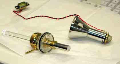
31 Analytical Scanning Electron Microscope CamScan 44
32 Electron Gun Magnetic Lens Scanning Coils Objectiv Lens Backscattered Electron Detector Anode Energy Dispersive X-Ray Detector Secondary Electron Detector Wave length Dispersive X-Ray Detector Stage with Specimen to the Vacuum Pump
33 Electron Gun (W-Cathode) Tungsten Cathode Wehnelt Cylinder (500 V more negative than the Cathode, Bias ) Heating Current (DC) V Crossover (20-50 µm) Electron beam source Anode grounding The crossover is belittlet projected on the sample by the electronic-optical system (minimal diameter of the beam: ca. 5 nm)
34 LaB 6 -Cathode (also: CeB 6 ): Graphite LaB 6 single crystal - indirect heating (because of the low conductivity of LaB 6 ) - lower work function than the W-cathode ( higher brightness) - demageable by ionic shooting ( high vacuum necessary) - expensive!
35 Field Emission-Cathode - W cathode with a fine apex - two anodes: 1. one to bring up the work function 2. one for the acceleration - high brightness - high vacuum necessary
36 Comparison of W-, LaB 6 -, and Field emission-cathods W LaB 6 FE work function /ev 4,5 2,7 4,5 crossover /µm (important for high resolution images) T cathod /K 2700 < emission current density /A/cm 2 ) gun Brightness /A/cm 2 sr vacuum /mbar service life /h >2000
37 Interaction of a high energy electron beam with material Primary Beam Auger Electrons Backscattered Electrons Cathode Luminescence Characteristic X-Ray Spectrum Secondary Electrons Specimen X-Ray Retardation Spectrum Absorbed Current
38 Principle of the image formation Beam synchronised scanning coils Amplifier Signal-Detector (SE or BE) Television image Specimen
39 Interaction volume of the electron beam (pear-like) primary beam Auger-electrons (up to 0,001µm)* Secondary Electrons (up to 0,01µm)* Backscattered Electrons (up to 0,1µm)* X-Ray (1-5µm)* *information depths


 Fe (20 kv) Al")
40 Dependence of the interaction volume on the acceleration voltage and material (simulations) Fe (10 kv) Au (20 kv) Fe (20 kv) Al (20 kv) Fe (30 kv) 1µm
41 Secondary Electrons: - inelastic scattered PE (Primary Electrons) - energy loss by interaction with orbital electrons or with the atomic nucleus - energy: < 50 ev - maximal emission depth: 5-50 nm high resolution images
42 Backscattered Electrons: - elastic and inelastic scattered PE - energy: 50 ev energyof thepe (e.g. 20 kev) - maximal emission depth: 0.1-6µm (dependent on the specimen) - intensity depends on the average atomic number of the material material contrast images - high interaction volume low resolution images
43 Auger Electrons: - energy characteristic for the element Auger Electron Spectroscopy (AES) 3. E 3 E Auger-Electron = E 1 -E 2 -E E 2 E 1
")

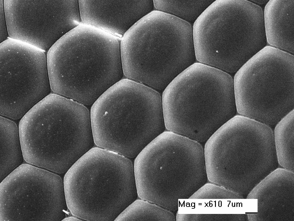
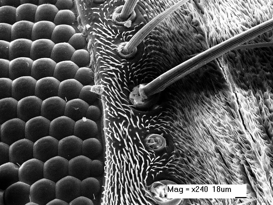
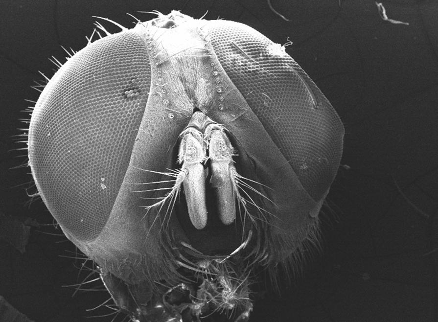
44 Cu-wire imbedded in solder SE-image (high resolution) BE-image (high Z-contrast) Cu Cu Cu Cu Z Pb > Z Sn > Z Cu


45 Backscattered electron images are less sensitive on charging: BE-image SE-image cause: the average energy of the backscattered electrons is higher
46 Cathode luminescence - visible and UV radiation - special detectors necessary -not formetals PE hν conduction band valence band
47 Characteristic X-Ray spectrum (without fine structure) O L γ M β N L β M α M K β L α L K α K
48 Energy range of the main series as a function of the atomic number: energy /kev K α K β L α M α L β Mosley s law: 1/λ = K (Z-1) 2 atomic number (K: constant, Z = atomic number)
49 Typical (characteristic) X-Ray spectrum (EDX) intensity Spectrum of Ag 6 GeS 4 Cl 2 energy /kev - sulfur (Z = 16) and chlorine (Z = 17) easily distinguishable (in contrast to X-Ray diffraction)
50 Competition Auger / X-Ray Rate of yield Auger X-Ray Z small X-Ray yield for light elements (B, C, N, O, F)

51 X-Ray Retardation Spectrum Intensity energy /kev - primary electrons are retarded by the electron clouds of the atoms -E max of the X-Ray s: e U accelerating voltage


52 Large area mapping (X-Ray-images) SE-Image Cu-Kαmapping Ni-Kαmapping Zn-Kαmapping 256x256 pixel, moving of the specimen holder
53 Electron Detectors 1. Secondary Electron (SE-) Detector Szintillator-Photomultiplier-Detector (Everhart-Thornley-Detector) amplifier videosignal photomultiplier light conductor scintillator metal net (+ 400V)


54 SE-detektor: SE-D SE-D
55 Principle of an EDX-detector p- i- n-conducting Si (Li) 3,8 ev hν + Si Si + + e e.g. Mn K α : 5894 ev X-Ray - + high voltage 5894/3.8 = 1550 electron hole pairs
56 WDX-Spectrometer: Scanning of a λ-range with one monochromator crystal Rowland circle detector axis of crystal travel monochromator crystal speciment (X-Ray source)
57 Detector s for WDX: two proportional counter switched in series 1. FPC, Flow proportional counter (for low energy X-Ray s) the counting gas (Ar / CH 4 ) flows through the counter (very thin polypropylen window, not leak-free for the counting gas) 2. SPC, Sealed proportional counter (for high energy X-Ray s) counting gas: Xenon / CO 2


58 WDX detector 4 monochromator crystals proportional counter
59 Comparison of EDX and WDX EDX WDX spectral resolution ev 10 ev specimen current A 10-7 A analysis time 1-2 min min spectrum develops simultaneous sequential
60 Sensitivity of EDX and WDX atomic percent EDX Be - window WDX atomic number
61 Comparison EDX - WDX I rel Ga L α Ga L β EDX Ge L α Ge L β WDX I rel Ga L α Ga L β Ge L α Ge L β (compound: GeGa 4 S 4 ) energy /kev


62 typical sample holder equipment typical preparation of small crystals condacting tabs (adhesive plastic with graphite)
63 Special preparation for insulating material: -metallisation with gold (sputtering process) high resolution images -carbon deposition (evaporation process) quantitative analysis


64 Sputter coater


65 Carbon coater
66 Applications: I) High resolution Images II) Qualitative and quantitative analysis

 3")
67 Twinning of Crystals PbS Na 2 Zn 2 (SeO 3 ) 3 3H 2 O


68 Morphology of crystals CuGa 3 S 5 K 2 In 12 Se 19 SnIn 4 S 4 CsIn 3 S 5


69 Quality control of small technical objects Compact disc Cantilever of an AFM
70
71
72
73 Quantitative analysis: The X-ray intensity of a characteristic element-line in the sample is compared with the intensity of this element-line in a standard standard: element or compound with known composition first approximation: I sample /I standard = c i but: corrections are necessary!!
74 Corrections: 1) Atomic number correction (Z-correction) a) stopping power of the material b) back-scatter power of the material 2) Absorption correction (A-correction) Different absorption of X-rays in different material 3) Fluorescence correction (F-correction) X-rays with high energy generate secondary radiation with lower energy I sample /I standard = k i = c i K Z K A K F
75 Further requirements for a quantitative measurement: - constant beam current during the measurement - defined take-off angle - plane surface - surface orientatet perpenticular to the beam - conductive surface
Electron Microprobe Analysis 1 Nilanjan Chatterjee, Ph.D. Principal Research Scientist
 12.141 Electron Microprobe Analysis 1 Nilanjan Chatterjee, Ph.D. Principal Research Scientist Massachusetts Institute of Technology Electron Microprobe Facility Department of Earth, Atmospheric and Planetary
Electron Microprobe Analysis 1 Nilanjan Chatterjee, Ph.D. Principal Research Scientist
 12.141 Electron Microprobe Analysis 1 Nilanjan Chatterjee, Ph.D. Principal Research Scientist Massachusetts Institute of Technology Electron Microprobe Facility Department of Earth, Atmospheric and Planetary
Chapter 3 (part 3) The Structures of Simple Solids
 The Structures of Simple Solids") CHM 511 chapter 3 page 1 of 9 Chapter 3 (part 3) The Structures of Simple Solids Rationalizing Structures Ionic radii As noted earlier, a reference value is needed. Usually oxygen is assumed to be 140
CHM 511 chapter 3 page 1 of 9 Chapter 3 (part 3) The Structures of Simple Solids Rationalizing Structures Ionic radii As noted earlier, a reference value is needed. Usually oxygen is assumed to be 140
EECS130 Integrated Circuit Devices
 EECS130 Integrated Circuit Devices Professor Ali Javey 8/30/2007 Semiconductor Fundamentals Lecture 2 Read: Chapters 1 and 2 Last Lecture: Energy Band Diagram Conduction band E c E g Band gap E v Valence
Chem 241. Lecture 21. UMass Amherst Biochemistry... Teaching Initiative
 Chem 241 Lecture 21 UMass Amherst Biochemistry... Teaching Initiative Announcement March 26 Second Exam Recap Calculation of space filling Counting atoms Alloys Ionic Solids Rock Salt CsCl... 2 ZnS Sphalerite/
ELEMENTARY BAND THEORY
 ELEMENTARY BAND THEORY PHYSICIST Solid state band Valence band, VB Conduction band, CB Fermi energy, E F Bloch orbital, delocalized n-doping p-doping Band gap, E g Direct band gap Indirect band gap Phonon
Ionic Bonding - Electrostatic Interactions and Polarization
 Ionic Bonding - Electrostatic Interactions and Polarization Chemistry 754 Solid State Chemistry Dr. Patrick Woodward Lecture #13 Born-Haber Cycle for NaCl It is energetically unfavorable for Na metal and
Chemistry Instrumental Analysis Lecture 8. Chem 4631
 Chemistry 4631 Instrumental Analysis Lecture 8 UV to IR Components of Optical Basic components of spectroscopic instruments: stable source of radiant energy transparent container to hold sample device
Semiconductors. SEM and EDAX images of an integrated circuit. SEM EDAX: Si EDAX: Al. Institut für Werkstoffe der ElektrotechnikIWE
 SEM and EDAX images of an integrated circuit SEM EDAX: Si EDAX: Al source: [Cal 99 / 605] M&D-.PPT, slide: 1, 12.02.02 Classification semiconductors electronic semiconductors mixed conductors ionic conductors
Chemical Analysis in TEM: XEDS, EELS and EFTEM. HRTEM PhD course Lecture 5
 Chemical Analysis in TEM: XEDS, EELS and EFTEM HRTEM PhD course Lecture 5 1 Part IV Subject Chapter Prio x-ray spectrometry 32 1 Spectra and mapping 33 2 Qualitative XEDS 34 1 Quantitative XEDS 35.1-35.4
Electron probe microanalysis - Electron microprobe analysis EPMA (EMPA) What s EPMA all about? What can you learn?
 What s EPMA all about? What can you learn?") Electron probe microanalysis - Electron microprobe analysis EPMA (EMPA) What s EPMA all about? What can you learn? EPMA - what is it? Precise and accurate quantitative chemical analyses of micron-size
Electron probe microanalysis - Electron microprobe analysis EPMA (EMPA) What s EPMA all about? What can you learn? EPMA - what is it? Precise and accurate quantitative chemical analyses of micron-size
Electrical Properties
 Electrical Properties Electrical Conduction R Ohm s law V = IR I l Area, A V where I is current (Ampere), V is voltage (Volts) and R is the resistance (Ohms or ) of the conductor Resistivity Resistivity,
Chemistry 311: Instrumentation Analysis Topic 2: Atomic Spectroscopy. Chemistry 311: Instrumentation Analysis Topic 2: Atomic Spectroscopy
 Topic 2b: X-ray Fluorescence Spectrometry Text: Chapter 12 Rouessac (1 week) 4.0 X-ray Fluorescence Download, read and understand EPA method 6010C ICP-OES Winter 2009 Page 1 Atomic X-ray Spectrometry Fundamental
Chemistry 101 Chapter 9 CHEMICAL BONDING. Chemical bonds are strong attractive force that exists between the atoms of a substance
 CHEMICAL BONDING Chemical bonds are strong attractive force that exists between the atoms of a substance Chemical Bonds are commonly classified into 3 types: 1. IONIC BONDING Ionic bonds usually form between
Ionic Bonding. Chem
 Whereas the term covalent implies sharing of electrons between atoms, the term ionic indicates that electrons are taken from one atom by another. The nature of ionic bonding is very different than that
Chemistry Instrumental Analysis Lecture 19 Chapter 12. Chem 4631
 Chemistry 4631 Instrumental Analysis Lecture 19 Chapter 12 There are three major techniques used for elemental analysis: Optical spectrometry Mass spectrometry X-ray spectrometry X-ray Techniques include:
MT Electron microscopy Scanning electron microscopy and electron probe microanalysis
 MT-0.6026 Electron microscopy Scanning electron microscopy and electron probe microanalysis Eero Haimi Research Manager Outline 1. Introduction Basics of scanning electron microscopy (SEM) and electron
Chapter 4 Scintillation Detectors
 Med Phys 4RA3, 4RB3/6R03 Radioisotopes and Radiation Methodology 4-1 4.1. Basic principle of the scintillator Chapter 4 Scintillation Detectors Scintillator Light sensor Ionizing radiation Light (visible,
= 6 (1/ nm) So what is probability of finding electron tunneled into a barrier 3 ev high?
 So what is probability of finding electron tunneled into a barrier 3 ev high?") STM STM With a scanning tunneling microscope, images of surfaces with atomic resolution can be readily obtained. An STM uses quantum tunneling of electrons to map the density of electrons on the surface
STM STM With a scanning tunneling microscope, images of surfaces with atomic resolution can be readily obtained. An STM uses quantum tunneling of electrons to map the density of electrons on the surface
Chapter 1 Overview of Semiconductor Materials and Physics
 Chapter 1 Overview of Semiconductor Materials and Physics Professor Paul K. Chu Conductivity / Resistivity of Insulators, Semiconductors, and Conductors Semiconductor Elements Period II III IV V VI 2 B
Energetics of Bond Formation
 BONDING, Part 4 Energetics of Bond Formation 167 Energetics of Covalent Bond Formation 168 1 169 Trends in Bond Energies the more electrons two atoms share, the stronger the covalent bond C C (837 kj)
Introduction to Engineering Materials ENGR2000. Dr.Coates
 Introduction to Engineering Materials ENGR2000 Chapter 18: Electrical Properties Dr.Coates 18.2 Ohm s Law V = IR where R is the resistance of the material, V is the voltage and I is the current. l R A
E12 UNDERSTANDING CRYSTAL STRUCTURES
 E1 UNDERSTANDING CRYSTAL STRUCTURES 1 Introduction In this experiment, the structures of many elements and compounds are rationalized using simple packing models. The pre-work revises and extends the material
Gaetano L Episcopo. Scanning Electron Microscopy Focus Ion Beam and. Pulsed Plasma Deposition
 Gaetano L Episcopo Scanning Electron Microscopy Focus Ion Beam and Pulsed Plasma Deposition Hystorical background Scientific discoveries 1897: J. Thomson discovers the electron. 1924: L. de Broglie propose
Mat E 272 Lecture 25: Electrical properties of materials
 Mat E 272 Lecture 25: Electrical properties of materials December 6, 2001 Introduction: Calcium and copper are both metals; Ca has a valence of +2 (2 electrons per atom) while Cu has a valence of +1 (1
Modern Optical Spectroscopy
 Modern Optical Spectroscopy X-Ray Microanalysis Shu-Ping Lin, Ph.D. Institute of Biomedical Engineering E-mail: splin@dragon.nchu.edu.tw Website: http://web.nchu.edu.tw/pweb/users/splin/ Backscattered
Energetic particles and their detection in situ (particle detectors) Part II. George Gloeckler
 Part II. George Gloeckler") Energetic particles and their detection in situ (particle detectors) Part II George Gloeckler University of Michigan, Ann Arbor, MI University of Maryland, College Park, MD Simple particle detectors Gas-filled
Energetic particles and their detection in situ (particle detectors) Part II George Gloeckler University of Michigan, Ann Arbor, MI University of Maryland, College Park, MD Simple particle detectors Gas-filled
Auger Electron Spectroscopy Overview
 Auger Electron Spectroscopy Overview Also known as: AES, Auger, SAM 1 Auger Electron Spectroscopy E KLL = E K - E L - E L AES Spectra of Cu EdN(E)/dE Auger Electron E N(E) x 5 E KLL Cu MNN Cu LMM E f E
EEE4106Z Radiation Interactions & Detection
 EEE4106Z Radiation Interactions & Detection 2. Radiation Detection Dr. Steve Peterson 5.14 RW James Department of Physics University of Cape Town steve.peterson@uct.ac.za May 06, 2015 EEE4106Z :: Radiation
Unit IV Semiconductors Engineering Physics
 Introduction A semiconductor is a material that has a resistivity lies between that of a conductor and an insulator. The conductivity of a semiconductor material can be varied under an external electrical
MT Electron microscopy Scanning electron microscopy and electron probe microanalysis
 MT-0.6026 Electron microscopy Scanning electron microscopy and electron probe microanalysis Eero Haimi Research Manager Outline 1. Introduction Basics of scanning electron microscopy (SEM) and electron
Chapter 11 Intermolecular Forces, Liquids, and Solids
 Chapter 11 Intermolecular Forces, Liquids, and Solids Dissolution of an ionic compound States of Matter The fundamental difference between states of matter is the distance between particles. States of
CME 300 Properties of Materials. ANSWERS: Homework 9 November 26, As atoms approach each other in the solid state the quantized energy states:
 CME 300 Properties of Materials ANSWERS: Homework 9 November 26, 2011 As atoms approach each other in the solid state the quantized energy states: are split. This splitting is associated with the wave
Advanced Lab Course. X-Ray Photoelectron Spectroscopy 1 INTRODUCTION 1 2 BASICS 1 3 EXPERIMENT Qualitative analysis Chemical Shifts 7
 Advanced Lab Course X-Ray Photoelectron Spectroscopy M210 As of: 2015-04-01 Aim: Chemical analysis of surfaces. Content 1 INTRODUCTION 1 2 BASICS 1 3 EXPERIMENT 3 3.1 Qualitative analysis 6 3.2 Chemical
R measurements (resistivity, magnetoresistance, Hall). Makariy A. Tanatar
. Makariy A. Tanatar") R measurements (resistivity, magnetoresistance, Hall). 590B Makariy A. Tanatar April 18, 2014 Resistivity Typical resistivity temperature dependence: metals, semiconductors Magnetic scattering Resistivities
R measurements (resistivity, magnetoresistance, Hall). 590B Makariy A. Tanatar April 18, 2014 Resistivity Typical resistivity temperature dependence: metals, semiconductors Magnetic scattering Resistivities
The Semiconductor in Equilibrium
 Lecture 6 Semiconductor physics IV The Semiconductor in Equilibrium Equilibrium, or thermal equilibrium No external forces such as voltages, electric fields. Magnetic fields, or temperature gradients are
Massachusetts Institute of Technology. Dr. Nilanjan Chatterjee
 Massachusetts Institute of Technology Dr. Nilanjan Chatterjee Electron Probe Micro-Analysis (EPMA) Imaging and micrometer-scale chemical compositional analysis of solids Signals produced in The Electron
Scanning Electron Microscopy
 Scanning Electron Microscopy Field emitting tip Grid 2kV 100kV Anode ZEISS SUPRA Variable Pressure FESEM Dr Heath Bagshaw CMA bagshawh@tcd.ie Why use an SEM? Fig 1. Examples of features resolvable using
Chapter 3. Crystal Binding
 Chapter 3. Crystal Binding Energy of a crystal and crystal binding Cohesive energy of Molecular crystals Ionic crystals Metallic crystals Elasticity What causes matter to exist in three different forms?
EECS143 Microfabrication Technology
 EECS143 Microfabrication Technology Professor Ali Javey Introduction to Materials Lecture 1 Evolution of Devices Yesterday s Transistor (1947) Today s Transistor (2006) Why Semiconductors? Conductors e.g
CHAPTER 18: Electrical properties
 CHAPTER 18: Electrical properties ISSUES TO ADDRESS... How are electrical conductance and resistance characterized? What are the physical phenomena that distinguish conductors, semiconductors, and insulators?
Midterm I Results. Mean: 35.5 (out of 100 pts) Median: 33 Mode: 25 Max: 104 Min: 2 SD: 18. Compare to: 2013 Mean: 59% 2014 Mean: 51%??
 Median: 33 Mode: 25 Max: 104 Min: 2 SD: 18. Compare to: 2013 Mean: 59% 2014 Mean: 51%??") Midterm I Results Mean: 35.5 (out of 100 pts) Median: 33 Mode: 25 Max: 104 Min: 2 SD: 18 Compare to: 2013 Mean: 59% 2014 Mean: 51%?? Crystal Thermodynamics and Electronic Structure Chapter 7 Monday, October
Midterm I Results Mean: 35.5 (out of 100 pts) Median: 33 Mode: 25 Max: 104 Min: 2 SD: 18 Compare to: 2013 Mean: 59% 2014 Mean: 51%?? Crystal Thermodynamics and Electronic Structure Chapter 7 Monday, October
SEM. Chemical Analysis in the. Elastic and Inelastic scattering. Chemical analysis in the SEM. Chemical analysis in the SEM
 THE UNIVERSITY Chemical Analysis in the SEM Ian Jones Centre for Electron Microscopy OF BIRMINGHAM Elastic and Inelastic scattering Electron interacts with one of the orbital electrons Secondary electrons,
Topics in the June 2006 Exam Paper for CHEM1901
 June 006 Topics in the June 006 Exam Paper for CHEM1901 Click on the links for resources on each topic. 006-J-: 006-J-3: 006-J-4: 006-J-5: 006-J-6: 006-J-7: 006-J-8: 006-J-9: 006-J-10: 006-J-11: 006-J-1:
Ch. 2: Energy Bands And Charge Carriers In Semiconductors
 Ch. 2: Energy Bands And Charge Carriers In Semiconductors Discrete energy levels arise from balance of attraction force between electrons and nucleus and repulsion force between electrons each electron
Review of Optical Properties of Materials
 Review of Optical Properties of Materials Review of optics Absorption in semiconductors: qualitative discussion Derivation of Optical Absorption Coefficient in Direct Semiconductors Photons When dealing
Advantages / Disadvantages of semiconductor detectors
 Advantages / Disadvantages of semiconductor detectors Semiconductor detectors have a high density (compared to gas detector) large energy loss in a short distance diffusion effect is smaller than in gas
XRF books: Analytical Chemistry, Kellner/Mermet/Otto/etc. 3 rd year XRF Spectroscopy Dr. Alan Ryder (R222, Physical Chemistry) 2 lectures:
 2 lectures:") 1 3 rd year XRF Spectroscopy Dr. Alan Ryder (R222, Physical Chemistry) 2 lectures: XRF spectroscopy 1 exam question. Notes on: www.nuigalway.ie/nanoscale/3rdspectroscopy.html XRF books: Analytical Chemistry,
1 3 rd year XRF Spectroscopy Dr. Alan Ryder (R222, Physical Chemistry) 2 lectures: XRF spectroscopy 1 exam question. Notes on: www.nuigalway.ie/nanoscale/3rdspectroscopy.html XRF books: Analytical Chemistry,
LN 3 IDLE MIND SOLUTIONS
 IDLE MIND SOLUTIONS 1. Let us first look in most general terms at the optical properties of solids with band gaps (E g ) of less than 4 ev, semiconductors by definition. The band gap energy (E g ) can
X-Ray Photoelectron Spectroscopy (XPS) Prof. Paul K. Chu
 Prof. Paul K. Chu") X-Ray Photoelectron Spectroscopy (XPS) Prof. Paul K. Chu X-ray Photoelectron Spectroscopy Introduction Qualitative analysis Quantitative analysis Charging compensation Small area analysis and XPS imaging
X-Ray Photoelectron Spectroscopy (XPS) Prof. Paul K. Chu X-ray Photoelectron Spectroscopy Introduction Qualitative analysis Quantitative analysis Charging compensation Small area analysis and XPS imaging
Part II: Thin Film Characterization
 Part II: Thin Film Characterization General details of thin film characterization instruments 1. Introduction to Thin Film Characterization Techniques 2. Structural characterization: SEM, TEM, AFM, STM
HW 2. CHEM 481 Chapters 3 & 5 Chapter 3. Energetics of Ionic Bonding
 HW 2. CHEM 481 Chapters 3 & 5 Chapter 3. Energetics of Ionic Bonding Name: 1. Give coordination number for both anion and cation of the following ionic lattices. a) CsCl Structure: b) Rock Salt Structure:
Lattice energy of ionic solids
 1 Lattice energy of ionic solids Interatomic Forces Solids are aggregates of atoms, ions or molecules. The bonding between these particles may be understood in terms of forces that play between them. Attractive
n i exp E g 2kT lnn i E g 2kT
 HOMEWORK #10 12.19 For intrinsic semiconductors, the intrinsic carrier concentration n i depends on temperature as follows: n i exp E g 2kT (28.35a) or taking natural logarithms, lnn i E g 2kT (12.35b)
CHEM*3440. X-Ray Energies. Bremsstrahlung Radiation. X-ray Line Spectra. Chemical Instrumentation. X-Ray Spectroscopy. Topic 13
 X-Ray Energies very short wavelength radiation 0.1Å to 10 nm (100 Å) CHEM*3440 Chemical Instrumentation Topic 13 X-Ray Spectroscopy Visible - Ultraviolet (UV) - Vacuum UV (VUV) - Extreme UV (XUV) - Soft
Lecture 1. OUTLINE Basic Semiconductor Physics. Reading: Chapter 2.1. Semiconductors Intrinsic (undoped) silicon Doping Carrier concentrations
 silicon Doping Carrier concentrations") Lecture 1 OUTLINE Basic Semiconductor Physics Semiconductors Intrinsic (undoped) silicon Doping Carrier concentrations Reading: Chapter 2.1 EE105 Fall 2007 Lecture 1, Slide 1 What is a Semiconductor? Low
Lecture 1 OUTLINE Basic Semiconductor Physics Semiconductors Intrinsic (undoped) silicon Doping Carrier concentrations Reading: Chapter 2.1 EE105 Fall 2007 Lecture 1, Slide 1 What is a Semiconductor? Low
Lecture 7: Extrinsic semiconductors - Fermi level
 Lecture 7: Extrinsic semiconductors - Fermi level Contents 1 Dopant materials 1 2 E F in extrinsic semiconductors 5 3 Temperature dependence of carrier concentration 6 3.1 Low temperature regime (T < T
Chapter 10 Review Packet
 Chapter 10 Review Packet Name 1. If water and carbon dioxide molecules did interact, what major intermolecular force will exist between these molecules? a) Hydrogen bonding b) London dispersion c) Dipole-dipole
Lecture 5. X-ray Photoemission Spectroscopy (XPS)
") Lecture 5 X-ray Photoemission Spectroscopy (XPS) 5. Photoemission Spectroscopy (XPS) 5. Principles 5.2 Interpretation 5.3 Instrumentation 5.4 XPS vs UV Photoelectron Spectroscopy (UPS) 5.5 Auger Electron
Lecture 5 X-ray Photoemission Spectroscopy (XPS) 5. Photoemission Spectroscopy (XPS) 5. Principles 5.2 Interpretation 5.3 Instrumentation 5.4 XPS vs UV Photoelectron Spectroscopy (UPS) 5.5 Auger Electron
CHAPTER 8 Ionic and Metallic Bonds
 CHAPTER 8 Ionic and Metallic Bonds Shows the kind of atoms and number of atoms in a compound. MgCl 2 NaCl CaCO 3 Al 2 O 3 Ca 3 (PO 4 ) 2 Chemical Formulas Al: Cl: counting atoms AlCl 3 Pb: N: O: Pb(NO
X-rays. X-ray Radiography - absorption is a function of Z and density. X-ray crystallography. X-ray spectrometry
 X-rays Wilhelm K. Roentgen (1845-1923) NP in Physics 1901 X-ray Radiography - absorption is a function of Z and density X-ray crystallography X-ray spectrometry X-rays Cu K α E = 8.05 kev λ = 1.541 Å Interaction
X-Ray Photoelectron Spectroscopy (XPS)
") X-Ray Photoelectron Spectroscopy (XPS) Louis Scudiero http://www.wsu.edu/~scudiero; 5-2669 Electron Spectroscopy for Chemical Analysis (ESCA) The basic principle of the photoelectric effect was enunciated
X-Ray Photoelectron Spectroscopy (XPS) Louis Scudiero http://www.wsu.edu/~scudiero; 5-2669 Electron Spectroscopy for Chemical Analysis (ESCA) The basic principle of the photoelectric effect was enunciated
Lecture 2: Atom and Bonding Semester /2013
 EMT 110 Engineering Materials Lecture 2: Atom and Bonding Semester 1 2012/2013 Atomic Structure Fundamental Concept Atoms are the structural unit of all engineering materials! Each atoms consist of nucleus
CHAPTER 2: ENERGY BANDS & CARRIER CONCENTRATION IN THERMAL EQUILIBRIUM. M.N.A. Halif & S.N. Sabki
 CHAPTER 2: ENERGY BANDS & CARRIER CONCENTRATION IN THERMAL EQUILIBRIUM OUTLINE 2.1 INTRODUCTION: 2.1.1 Semiconductor Materials 2.1.2 Basic Crystal Structure 2.1.3 Basic Crystal Growth technique 2.1.4 Valence
Introduction to X-ray Photoelectron Spectroscopy (XPS) XPS which makes use of the photoelectric effect, was developed in the mid-1960
 XPS which makes use of the photoelectric effect, was developed in the mid-1960") Introduction to X-ray Photoelectron Spectroscopy (XPS) X-ray Photoelectron Spectroscopy (XPS), also known as Electron Spectroscopy for Chemical Analysis (ESCA) is a widely used technique to investigate
Introduction to X-ray Photoelectron Spectroscopy (XPS) X-ray Photoelectron Spectroscopy (XPS), also known as Electron Spectroscopy for Chemical Analysis (ESCA) is a widely used technique to investigate
EE 5344 Introduction to MEMS CHAPTER 5 Radiation Sensors
 EE 5344 Introduction to MEMS CHAPTER 5 Radiation Sensors 5. Radiation Microsensors Radiation µ-sensors convert incident radiant signals into standard electrical out put signals. Radiant Signals Classification
Chapter 9. Electron mean free path Microscopy principles of SEM, TEM, LEEM
 Chapter 9 Electron mean free path Microscopy principles of SEM, TEM, LEEM 9.1 Electron Mean Free Path 9. Scanning Electron Microscopy (SEM) -SEM design; Secondary electron imaging; Backscattered electron
Energy Spectroscopy. Excitation by means of a probe
 Energy Spectroscopy Excitation by means of a probe Energy spectral analysis of the in coming particles -> XAS or Energy spectral analysis of the out coming particles Different probes are possible: Auger
Imaging Methods: Scanning Force Microscopy (SFM / AFM)
") Imaging Methods: Scanning Force Microscopy (SFM / AFM) The atomic force microscope (AFM) probes the surface of a sample with a sharp tip, a couple of microns long and often less than 100 Å in diameter.
Imaging Methods: Scanning Force Microscopy (SFM / AFM) The atomic force microscope (AFM) probes the surface of a sample with a sharp tip, a couple of microns long and often less than 100 Å in diameter.
ELECTRONIC DEVICES AND CIRCUITS SUMMARY
 ELECTRONIC DEVICES AND CIRCUITS SUMMARY Classification of Materials: Insulator: An insulator is a material that offers a very low level (or negligible) of conductivity when voltage is applied. Eg: Paper,
CHEMISTRY XL-14A CHEMICAL BONDS
 CHEMISTRY XL-14A CHEMICAL BONDS July 16, 2011 Robert Iafe Office Hours 2 July 18-July 22 Monday: 2:00pm in Room MS-B 3114 Tuesday-Thursday: 3:00pm in Room MS-B 3114 Chapter 2 Overview 3 Ionic Bonds Covalent
SOLID STATE PHYSICS PHY F341. Dr. Manjuladevi.V Associate Professor Department of Physics BITS Pilani
 SOLID STATE PHYSICS PHY F341 Dr. Manjuladevi.V Associate Professor Department of Physics BITS Pilani 333031 manjula@bits-pilani.ac.in Characterization techniques SEM AFM STM BAM Outline What can we use
Reference literature. (See: CHEM 2470 notes, Module 8 Textbook 6th ed., Chapters )
") September 17, 2018 Reference literature (See: CHEM 2470 notes, Module 8 Textbook 6th ed., Chapters 13-14 ) Reference.: https://slideplayer.com/slide/8354408/ Spectroscopy Usual Wavelength Type of Quantum
September 17, 2018 Reference literature (See: CHEM 2470 notes, Module 8 Textbook 6th ed., Chapters 13-14 ) Reference.: https://slideplayer.com/slide/8354408/ Spectroscopy Usual Wavelength Type of Quantum
Atoms & Their Interactions
 Lecture 2 Atoms & Their Interactions Si: the heart of electronic materials Intel, 300mm Si wafer, 200 μm thick and 48-core CPU ( cloud computing on a chip ) Twin Creeks Technologies, San Jose, Si wafer,
Lecture 18. New gas detectors Solid state trackers
 Lecture 18 New gas detectors Solid state trackers Time projection Chamber Full 3-D track reconstruction x-y from wires and segmented cathode of MWPC z from drift time de/dx information (extra) Drift over
Electrical material properties
 Electrical material properties U = I R Ohm s law R = ρ (l/a) ρ resistivity l length σ = 1/ρ σ conductivity A area σ = n q μ n conc. of charge carriers q their charge μ their mobility μ depends on T, defects,
Forming Chemical Bonds
 Forming Chemical Bonds Chemical Bonds Three basic types of bonds 2012 Pearson Education, Inc. Ionic Electrostatic attraction between ions. Covalent Sharing of electrons. Metallic Metal atoms bonded to
SOLID STATE CHEMISTRY
 SOLID STATE CHEMISTRY Crystal Structure Solids are divided into 2 categories: I. Crystalline possesses rigid and long-range order; its atoms, molecules or ions occupy specific positions, e.g. ice II. Amorphous
MS482 Materials Characterization ( 재료분석 ) Lecture Note 4: XRF
 Lecture Note 4: XRF") 2016 Fall Semester MS482 Materials Characterization ( 재료분석 ) Lecture Note 4: XRF Byungha Shin Dept. of MSE, KAIST 1 Course Information Syllabus 1. Overview of various characterization techniques (1 lecture)
2016 Fall Semester MS482 Materials Characterization ( 재료분석 ) Lecture Note 4: XRF Byungha Shin Dept. of MSE, KAIST 1 Course Information Syllabus 1. Overview of various characterization techniques (1 lecture)
M2 TP. Low-Energy Electron Diffraction (LEED)
") M2 TP Low-Energy Electron Diffraction (LEED) Guide for report preparation I. Introduction: Elastic scattering or diffraction of electrons is the standard technique in surface science for obtaining structural
M2 TP Low-Energy Electron Diffraction (LEED) Guide for report preparation I. Introduction: Elastic scattering or diffraction of electrons is the standard technique in surface science for obtaining structural
Emphasis on what happens to emitted particle (if no nuclear reaction and MEDIUM (i.e., atomic effects)
") LECTURE 5: INTERACTION OF RADIATION WITH MATTER All radiation is detected through its interaction with matter! INTRODUCTION: What happens when radiation passes through matter? Emphasis on what happens
LECTURE 5: INTERACTION OF RADIATION WITH MATTER All radiation is detected through its interaction with matter! INTRODUCTION: What happens when radiation passes through matter? Emphasis on what happens
Chapter 3 Engineering Science for Microsystems Design and Fabrication
 Lectures on MEMS and MICROSYSTEMS DESIGN and MANUFACTURE Chapter 3 Engineering Science for Microsystems Design and Fabrication In this Chapter, we will present overviews of the principles of physical and
Chem 241. Lecture 23. UMass Amherst Biochemistry... Teaching Initiative
 Chem 241 Lecture 23 UMass Amherst Biochemistry... Teaching Initiative Announcement Mistake we have class on the 3 rd not 4 th Exam 3 Originally scheduled April 23 rd (Friday) What about April 26 th (Next
The Electromagnetic Properties of Materials
 The Electromagnetic Properties of Materials Electrical conduction Metals Semiconductors Insulators (dielectrics) Superconductors Magnetic materials Ferromagnetic materials Others Photonic Materials (optical)
Chapter 4: Bonding in Solids and Electronic Properties. Free electron theory
 Chapter 4: Bonding in Solids and Electronic Properties Free electron theory Consider free electrons in a metal an electron gas. regards a metal as a box in which electrons are free to move. assumes nuclei
2008 Brooks/Cole 2. Frequency (Hz)
") Electromagnetic Radiation and Matter Oscillating electric and magnetic fields. Magnetic field Electric field Chapter 7: Electron Configurations and the Periodic Table Traveling wave moves through space
Electromagnetic Radiation and Matter Oscillating electric and magnetic fields. Magnetic field Electric field Chapter 7: Electron Configurations and the Periodic Table Traveling wave moves through space
Engineering 2000 Chapter 8 Semiconductors. ENG2000: R.I. Hornsey Semi: 1
 Engineering 2000 Chapter 8 Semiconductors ENG2000: R.I. Hornsey Semi: 1 Overview We need to know the electrical properties of Si To do this, we must also draw on some of the physical properties and we
Because light behaves like a wave, we can describe it in one of two ways by its wavelength or by its frequency.
 Light We can use different terms to describe light: Color Wavelength Frequency Light is composed of electromagnetic waves that travel through some medium. The properties of the medium determine how light
PHYSICS nd TERM Outline Notes (continued)
") PHYSICS 2800 2 nd TERM Outline Notes (continued) Section 6. Optical Properties (see also textbook, chapter 15) This section will be concerned with how electromagnetic radiation (visible light, in particular)
PHYSICS 2800 2 nd TERM Outline Notes (continued) Section 6. Optical Properties (see also textbook, chapter 15) This section will be concerned with how electromagnetic radiation (visible light, in particular)
Secondary Ion Mass Spectroscopy (SIMS)
") Secondary Ion Mass Spectroscopy (SIMS) Analyzing Inorganic Solids * = under special conditions ** = semiconductors only + = limited number of elements or groups Analyzing Organic Solids * = under special
Secondary Ion Mass Spectroscopy (SIMS) Analyzing Inorganic Solids * = under special conditions ** = semiconductors only + = limited number of elements or groups Analyzing Organic Solids * = under special
Part A. Answer all questions in this part.
 Part A Directions (1-20): For each statement or question, record on your separate answer sheet the number of the word or expression that, of those given, best completes the statement or answers the question.
 lectures accompanying the book: Solid State Physics: An Introduction, by Philip ofmann (2nd edition 2015, ISBN-10: 3527412824, ISBN-13: 978-3527412822, Wiley-VC Berlin. www.philiphofmann.net 1 Bonds between
lattice formation from gaseous ions
 BORN HABER CYCLES The Born Haber cycles is an adaption of Hess s law to calculate lattice enthalpy from other data The lattice enthalpy cannot be determined directly. We calculate it indirectly by making
Chem 481 Lecture Material 3/20/09
 Chem 481 Lecture Material 3/20/09 Radiation Detection and Measurement Semiconductor Detectors The electrons in a sample of silicon are each bound to specific silicon atoms (occupy the valence band). If
Types of Bonding : Ionic Compounds. Types of Bonding : Ionic Compounds
 Types of Bonding : Ionic Compounds Ionic bonding involves the complete TRANSFER of electrons from one atom to another. Usually observed when a metal bonds to a nonmetal. - - - - - - + + + + + + + + + +
Chapter 11. Intermolecular Forces and Liquids & Solids
 Chapter 11 Intermolecular Forces and Liquids & Solids The Kinetic Molecular Theory of Liquids & Solids Gases vs. Liquids & Solids difference is distance between molecules Liquids Molecules close together;
Semiconductor X-Ray Detectors. Tobias Eggert Ketek GmbH
 Semiconductor X-Ray Detectors Tobias Eggert Ketek GmbH Semiconductor X-Ray Detectors Part A Principles of Semiconductor Detectors 1. Basic Principles 2. Typical Applications 3. Planar Technology 4. Read-out
Semiconductor-Detectors
 Semiconductor-Detectors 1 Motivation ~ 195: Discovery that pn-- junctions can be used to detect particles. Semiconductor detectors used for energy measurements ( Germanium) Since ~ 3 years: Semiconductor
Chapter 9 Ionic and Covalent Bonding
 Chem 1045 Prof George W.J. Kenney, Jr General Chemistry by Ebbing and Gammon, 8th Edition Last Update: 06-April-2009 Chapter 9 Ionic and Covalent Bonding These Notes are to SUPPLIMENT the Text, They do
CHEMISTRY - BROWN 13E CH.7 - PERIODIC PROPERTIES OF THE ELEMENTS
 !! www.clutchprep.com CONCEPT: EFFECTIVE NUCLEAR CHARGE & SLATER S RULES When looking at any particular electron within an atom it experiences two major forces. A(n) force from the nucleus and a(n) force