SEM Doctoral Course MS-636. April 11-13, 2016
|
|
|
- Cory Bates
- 5 years ago
- Views:
Transcription


 on the observed area often results from a low system vacuum level in combination with existing surface contaminants.")

1 Thomas LaGrange, Ph.D. Faculty Lecturer and Senior Staff Scientist Electron Sources, Optics and Detectors SEM Doctoral Course MS-636 April 11-13, 2016 Summary Electron propagation is only possible through vacuum. The vacuum level varies between regions of the electron microscope; the highest vacuum level (<10-7 Pa or 10-9 mbar) being in the gun where electrons are emitted and accelerated and is required to keep source and accelerator clean. The specimen area also requires a high vacuum level to reduce contamination, which is especially important for chemical analysis that requires the electron beam to rest in the same area for a long time. Hydrocarbon build up (contamination) on the observed area often results from a low system vacuum level in combination with existing surface contaminants. Turbo-molecular and oil-diffusion pumps for high vacuum cannot work against atmospheric pressure and they require a mechanical prevacuum pump to back them for proper and efficient operation. Electron beams are generated either by thermal emission or field emission. Field emission sources provide lower energy spread and high coherence required high resolution spatial resolution imaging and electron spectroscopy. Electrons are focused by simple round magnetic lenses which properties resemble the optical properties of a wine glass. Unlike in light optics the wavelength (2pm for 300kV) is not the resolution limiting factor. Lens aberrations however and instabilities of the electronics (lens currents etc.) limit the resolution of even the best and most expensive transmission electron microscopes to about 50pm. Recording an image means detecting electrons. Depending on their energy electrons can be detected by different detectors. A high detector efficiency and a high signal to noise ratio allows faster recording and reduces the exposure (beam damage) of the sample to the electron beam. A high linearity and high dynamic range permits to quantify images and to record high and low intensities in one image (important for diffraction experiments). 2 1

2 Components of a scanning electron microscope Scan coils 1. Electron propagation is only possible through vacuum! 2. Need a good vacuum system to reduce contamination! 3 Outline: This section of the course describes main components of the scanning electron microscope: pumping systems, electron sources, electron optics and detectors. 1) Pumping Systems 2) Electron sources 3) Electron optics A. Basics B. Magnetic Lens C. Aberrations and Spatial Resolution Limits in a SEM D. Modern SEMs 4) Detectors A. Secondary electrons B. Back scattered electrons C. X-ray detectors 4 2

 Pumping system: Primary vacuum 6 Rotary vane pump Uses oil (wet) which can be a source of contamination Noisy but not active all of the time (buffer tank backing) Cheap and")
3 1) Pumping system: block diagram Gun Ion Pump Column Ion Pump Buffer/ Reservoir Tank SEM Column and Sample Chamber Electron Gun Gun Valve Secondary pump valve Diffusion Pump Primary pump Valve Air Primary vacuum (>0.1 Pa) Mechanical pump Secondary vacuum (<10-4 Pa) Oil diffusion pump Turbomolecular pump High and ultra-high vacuum Gun & specimen area (<10-6 Pa) Ion getter pump Cold trap 5 Mechanical Rough Pump Vent Valve 1) Pumping system: Primary vacuum 6 Rotary vane pump Uses oil (wet) which can be a source of contamination Noisy but not active all of the time (buffer tank backing) Cheap and low maintenance Scroll pumps No oils or sources of contamination, Dry Expensive Lower ultimate vacuum pressure (10-2 torr) High maintenance, scrolls need to be yearly 3
 Best with")

4 1) Pumping system: Secondary vacuum Oil diffusion pump Vibration free cheap, reliable and low maintenance Possible Contamination sources: oil vapor High pumping capacity (>500 l/s) Best with cold trap (limits oil vapor migration) 7 1 ) Pumping system: Secondary vacuum Turbomolecular pumps Rotation speed 20-50,000 rpm Magnetic bearings Pumping volumes l/s No oils or sources of contamination 8 4
 no vibrations No exit ; no pumping improves")


5 1 ) Pumping system: High / Ultra-high vacuum Ion getter pump (IGP) no vibrations No exit ; no pumping improves vacuum by trapping gas molecules in sputtered Ti layers Requires High Vacuum via secondary pumping before using and for proper operation 9 2) Electron Sources LaB 6 Cathode Tungsten Field Emission Tip


6 2) Electron Sources: Comparison of Sources 11 2) Electron Sources: thermionic gun Electron boil from surface.heated to overcome the work function to push electrons in vacuum level Tungsten wire heated to ~2800K LaB 6 crystal heated to 1900K Main advantages: simple, cheap, no high vacuum required and maintenance friendly Disadvantages: low brightness, high energy spread and large source size ( m) 12 6
 Extended Schottky emission thermally assisted field emission Cold field emission tunnel effect (quantum tunnelling) Hot Schottky Cold Schottky Hot FE")
 high coherence, high brightness -> higher resolution at lower energies Disadvantages: expensive, high vacuum necessary cold emission needs flushing (cleaning) after 8 hrs Thermally assisted")
7 Increasing Temperature 300 K 1700 K 10/29/2016 2) Electron Sources: Emission of electrons metal vacuum (with electrical field) Increasing electric field Thermionic emission Schottky emission field-enhanced thermionic emission (10 8 V/m) Extended Schottky emission thermally assisted field emission Cold field emission tunnel effect (quantum tunnelling) Hot Schottky Cold Schottky Hot FE Cold FE 13 2) Electron Sources: Field emission guns (emitter) Cathodes (tips) Cold field emission (E 10 9 V/m) W single crystal with a sharp tip (radius ~25nm) Advantages Small energy dispersion (<0.1eV) high coherence, high brightness -> higher resolution at lower energies Disadvantages: expensive, high vacuum necessary cold emission needs flushing (cleaning) after 8 hrs Thermally assisted emission: Schottky effect Large tip size W/Zr tip at K ZrO complexes lower work function Continuous operation self-cleaning ZrO 2 reservoir 14 7

8 2) Electron Sources: Field emission guns (extraction) First anode (extractor) Some kv V/m Second anode Final acceleration Grounded- to slight voltage for focusing and increasing electron current Characteristics Tip and anodes form an electrostatic condensor Cross-over (virtual source) size is Ø~5nm 15 3) Electron Optics: Basics Object plane Focal plane Image plane Carter/Williams 16 8
9 3) Electron Optics: Basics Parallel beams are focused to one point in the focal plane Object plane Parallel beams are focused to one point in the focal plane Focal plane Image plane tiré de Carter/Williams 17 3) Electron Optics: basics Image plane 1. Over-focus 2. Focus 3. Under-focus tiré de Carter/Williams 18 9
 Electron Optics: Condenser lens system, SEM First Condenser Lens (C1) Defines probe size Small spot <-> small current Large spot <-> high current Used to change Probe Current")
10 3) Electron Optics: Basics Apertures Angle limiting apertures Defines convergence angle Used to change depth of field, current, and probe size in combination with condenser lens system tiré de Carter/Williams 19 3) Electron Optics: Condenser lens system, SEM First Condenser Lens (C1) Defines probe size Small spot <-> small current Large spot <-> high current Used to change Probe Current 20 10


11 3) Electron Optics: Condenser lens system, SEM Double Condenser Lens systems in modern microscopes allow increased flexibility in controlling probe current and convergence angle on the sample 21 3) Magnetic Lenses: Lenses for light, lenses for electrons Light: glass lenses deflection of light through changing refraction index Electrons: (charged particles) Electrostatic lenses Magnetic lenses: Lorentz Force! Variable focus (no moving parts) Tunable correctors (astigmatism) 22 11

 Magnetic lens iron Pole piece e-beam coil Electron optics: no sharp interface at lens «surface» Pole piece metal cone that confines the magnetic field")
12 3) Magnetic Lens: Electrons in a magnetic field Optical axis a Homogeneus field, a small Component of v // B almost unchanged Component of v B: v r << v Spiral with radius r = m vr/eb All electrons crossing the axis in one point are focused into the same point, a, v r Focal length depends on B increasing B lowers f Image rotation! 23 3) Magnetic lens iron Pole piece e-beam coil Electron optics: no sharp interface at lens «surface» Pole piece metal cone that confines the magnetic field Image rotation! No (simple) divergent lens! «multi-poles» lenses Correction of aberrations
 Magnetic lens Field with rotational symmetry Lorenz Force : F = -e v ^ B electrons on optical axis: F = 0 electrons not on optical axis : deviated")

13 Out of focus astigmatic Ok! Clichés: P.-A. Buffat 10/29/2016 3) Magnetic lens Field with rotational symmetry Lorenz Force : F = -e v ^ B electrons on optical axis: F = 0 electrons not on optical axis : deviated **optical axis is the symmetry axis Scherzer 1936: Magnetic lens with rotational symmetry: Aberration coefficients: C s : spherical C c : chromatical Always positive!! Resolution limit: D res 3/ 4 1/ Cs Example: = nm, C s = 1 mm D res = = 1.8Å 25 3) Electron Optics: aberrations: Lens aberrations Focus Astigmatism sperical and chromatical aberrations Can be corrected or minimized Physical limits Diffraction limited resolution 26 13

14 2) Electron Optics: Chromatic Aberration Focal length varies with energy critical for nonmonochromatic beams (advantage for FE guns) 27 3) Electron Optics: Spherical Aberration Focal length varies with distance from optical axis, i.e., rays from the center to edge of the lens have different focal points Image of the object is dispersed (or blurred) along the optical axis Circle of least confusion d s = ½ C s a
 Electron Optics: Aberration Correctors Astigmatism: Light optics: Correction with cylindrical")

15 3) Electron Optics: Aberrations-astigmatism Astigmatism: focal length varies in different planes. This cause the image to be direction 29 3) Electron Optics: Aberration Correctors Astigmatism: Light optics: Correction with cylindrical lenses Electron optics: Correction with quadrupole lenses, 2 quadrupole lenses under 45 degree allow to control strength and direction of correction Spherical Aberration: Light optics: correction with combination of convergent and divergent lenses Electron optics: Correction with hexapole or quadrupole and octopole lenses 30 15
 Electron Optics: Resolution Raleigh s Criterion: Diffraction Limited")

16 3) Electron Optics: Resolution Spatial resolution depends on the size of the interaction volume Interaction volume differs material, accelerating voltage, spot size Different particles have different interaction volumes sizes and thus different resolution for the same microscope settings 31 2) Electron Optics: Resolution Raleigh s Criterion: Diffraction Limited Resolution d Green light : 532 nm, (objective collection angle)~1 rad Airy Diffraction Disks n= 1.7 for oil immersion lens ** d=190nm Electrons 10 kev : nm n=1 for vacuum =0.1 rad given SEM geometry **d=0.075 nm Lens aberrations limit spatial resolution to ~1 nm d = 0.61 n sin θ = 0.61 λ Thermionic SEM limited by source brightness FEG SEM limited by lens aberrations β 32 16

17 Resolution Résolution (nm) 10/29/2016 3) Electron Optics: Resolution Limits for a modern SEM d ech d d 2 g 2 sph d 2 ch d 2 d 33 3) Electron Optics: Resolution at Low kv Low voltage, high resolution Basse tension/haute résolution: Observation - observation of the de la real surface surface réelle Uncoated - échantillons samples non-métallisés - faible endommagement dû au Very faisceau little beam damage 1985 FE LaB 6 W High Haute voltage, tension/haute high résolution: resolution Edge - effets effects, de bord fine details not resolved - détails fins non-résolus - fort endommagement dû au Beam faisceau damage Tension High Tension d'accélération Voltage, (kv) kv 34 17
")
 Electron Optics: Modern Microscopes")
18 3) Electron Optics: FEG Microscopes Specifications of CIME FEI XL kv Schottky FEG SE imaging resolution: 2nm at 30 kv; 8nm at 1 kv Equipped with: Everhart- Thornley secondary-electron (SE) detector; backscattered electron (BE) detector; EDAX Si(Li) EDX detector with ultra-thin window for light element analysis Installed and operating since ) Electron Optics: Modern Microscopes 36 18


19 3) Electron Optics: Modern Microscopes 37 3) Electron Optics: Modern Microscopes -Conventional Mode magnetic field inside pole-piece 38 19

 39 3) Electron Optics: Modern Microscopes BSE at 2kV: ~1nm resolution BSE at 500V: ~5 nm")
20 3) Electron Optics: Immersion lens Modern Low kv SEMs specimen inside lens A small specimen sits inside the lens gap Has very short focal distance, range of 2 to 5 mm Short focal distance means low aberrations, small probe sizes, and high resolution Secondary electrons spiral upward in the strong magnetic field of the lens and are collected by the detector positioned above the lens (**In-Lens Detectors) 39 3) Electron Optics: Modern Microscopes BSE at 2kV: ~1nm resolution BSE at 500V: ~5 nm resolution 40 20

21 3) Electron Optics: Modern Microscopes MERLIN Analytical power for the sub-nanometer world 41 3) Electron Optics: Modern Microscopes MERLIN Analytical power for the sub-nanometer world High stability field emitter cathode Maximum probe current 300 na Beam Double Booster condenser lens Brightness Aperture independent of the electron probe probe current adjustment maintained for low landing energies Energy selective Backscatter detector (EsB) In-lens Secondary Electron detector GEMINI II final lens GEMINI II design Complete detection system Proven GEMINI final lens design New double condenser lens for highest probe current possibilities (300 na) Beam booster technology maintains brightness of all electron probes including low landing energies True on-axis in-lens SE and BSE detectors 42 21


22 Combined Deceleration of high voltage electrons and the filtering of aberrated electrons provides improved resolution at Low kv imaging 43 3) Electron Optics: Modern Microscopes 44 22


23 3) Electron Optics: Modern Microscopes 45 3) Electron Optics: Modern Microscopes 46 23

, SE")

24 3) Electron Optics: Modern Microscopes 4) Detectors: SEM, signals Backscattered electrons photons IR,UV,vis. inelastic elastic e-beam Secondary electrons X-rays Absorbed current, EBIC Auger electrons Secondary electrons (~0-30eV), SE Backscattered electrons (~evo), BSE Photons: visible, UV, IR, X-rays Auger electrons Phonons, Heating Absorbtion of incident electrons (EBIC-Current) 48 24
25 4) Detectors: SEM imaging with electrons Energy spectrum of electrons leaving the sample SE: secondary electrons 0-50eV BSE: backscattered electrons E>50eV 49 4) Electron detectors: Secondary Electrons Electrons with low energy (0-50eV) leaving the sample surface Intensity depends on inclination of the surface topography 50 25
 attracts the SE toward the detector, the 10kV post acceleration give them enough energy to")


26 4) Electron detectors: Secondary Electrons Photomultiplier Everhart-Thornley detector Collects and detects lower energy (<100eV) electrons: The positive collector voltage ( +200 à +400V) attracts the SE toward the detector, the 10kV post acceleration give them enough energy to create a bunch of photons for each SE 51 4) Electron detectors: In-lens SE In-lens SE (Secondary Electron detector) Topographical information with on-axis in-lens SE detector On axis In-Lens SE detector 52 Complete detection system: Small collection angle Topographical information Unique double in-lens detection Acquisition of pure secondary and backscatter electron signals Separation of compositional, topographical and crystalline surface information High resolution (low working distances, less spherical aberration and collection geometry limits SE2 and SE3 electrons) 26
 ~composition contrast (Z) Nb 3 Sn")

")
27 4) Electron detectors: backscattered electrons Electrons with high energy (~Eo) backscattered from below the surface Intensity depends on density (atomic weight) ~composition contrast (Z) Nb 3 Sn in Cu matrix 53 5) Electron detectors: Semiconductor BSE BSE semiconductor detector: a silicon diode with a p-n junction close to its surface collects the BSE (3.8eV per electron hole pair) large collection angle slow (poor at TV frequency) some diodes are split in 2 or 4 quadrants to bring spatial BSE distribution info Detects higher energy (>5kV) electrons: SEM backscattered electrons 55 27
 Compositional contrast with on-axis in column EsB detector Si 3")


28 4) Electron detectors: In-lens BSE (EsB) Energy filtering grid EsB (Energy selective Backscatter detector) Compositional contrast with on-axis in column EsB detector Si 3 N 4 TiN Si Ti 56 GEMINI II design Complete detection system Unique double in-lens detection Acquisition of pure secondary and backscatter electron signals Separation of compositional, topographical and crystalline surface information On axis In-Lens EsB detector Small collection angle Loss BSE more Z-contrast information Bias control for improved selectivity and contrast Electron matter interactions in a thin sample: Inelastic Scattering Characteristic X-rays Energy Dispersive Spectroscopy K- edges L- edges 57 28


29 4) X-ray Detectors: Silicon Lithium X-Ray energy converted to electrical charges: 3.8eV / electron-hole pair in average Must operate an optimum working distance for highest solid angle (known take-off angle) electronic noise+ imperfect charge collection: 150 ev resolution / Mn Ka line Detector acts like a diode: at room temperature the leak current for 1000V would be too high! The FET produces less noise if cooled and Li migrates at room temperature, which is also why the detector is cooled using LN2 58 4) X-ray Detectors: Silicon Drift Detector (SDD) Still 3.8eV / electron-hole pair in average electronic noise+ imperfect charge collection: 129 ev resolution / Mn Ka line The optimized FET design has lower noise than old generation SiLi detectors, so it can be cooled with thermoelectric cooler (PTEC) Improved light element sensitivity Windowless systems Conversion of X-rays in to recorded counts 59 29

30 QUESTIONS? 60 30
Basic structure of SEM
 Table of contents Basis structure of SEM SEM imaging modes Comparison of ordinary SEM and FESEM Electron behavior Electron matter interaction o Elastic interaction o Inelastic interaction o Interaction
Electron Microprobe Analysis 1 Nilanjan Chatterjee, Ph.D. Principal Research Scientist
 12.141 Electron Microprobe Analysis 1 Nilanjan Chatterjee, Ph.D. Principal Research Scientist Massachusetts Institute of Technology Electron Microprobe Facility Department of Earth, Atmospheric and Planetary
Electron Microprobe Analysis 1 Nilanjan Chatterjee, Ph.D. Principal Research Scientist
 12.141 Electron Microprobe Analysis 1 Nilanjan Chatterjee, Ph.D. Principal Research Scientist Massachusetts Institute of Technology Electron Microprobe Facility Department of Earth, Atmospheric and Planetary
MSE 321 Structural Characterization
 Optical Microscope Plan Lenses In an "ideal" single-element lens system all planar wave fronts are focused to a point at distance f from the lens; therefore: Image near the optical axis will be in perfect
Scanning Electron Microscopy
 Scanning Electron Microscopy Field emitting tip Grid 2kV 100kV Anode ZEISS SUPRA Variable Pressure FESEM Dr Heath Bagshaw CMA bagshawh@tcd.ie Why use an SEM? Fig 1. Examples of features resolvable using
= 6 (1/ nm) So what is probability of finding electron tunneled into a barrier 3 ev high?
 So what is probability of finding electron tunneled into a barrier 3 ev high?") STM STM With a scanning tunneling microscope, images of surfaces with atomic resolution can be readily obtained. An STM uses quantum tunneling of electrons to map the density of electrons on the surface
STM STM With a scanning tunneling microscope, images of surfaces with atomic resolution can be readily obtained. An STM uses quantum tunneling of electrons to map the density of electrons on the surface
Part II: Thin Film Characterization
 Part II: Thin Film Characterization General details of thin film characterization instruments 1. Introduction to Thin Film Characterization Techniques 2. Structural characterization: SEM, TEM, AFM, STM
Practical course in scanning electron microscopy
 Practical course in scanning electron microscopy Fortgeschrittenen Praktikum an der Technischen Universität München Wintersemester 2017/2018 Table of contents 1. Introduction 3 2. Formation of an electron
AP5301/ Name the major parts of an optical microscope and state their functions.
 Review Problems on Optical Microscopy AP5301/8301-2015 1. Name the major parts of an optical microscope and state their functions. 2. Compare the focal lengths of two glass converging lenses, one with
Gaetano L Episcopo. Scanning Electron Microscopy Focus Ion Beam and. Pulsed Plasma Deposition
 Gaetano L Episcopo Scanning Electron Microscopy Focus Ion Beam and Pulsed Plasma Deposition Hystorical background Scientific discoveries 1897: J. Thomson discovers the electron. 1924: L. de Broglie propose
M2 TP. Low-Energy Electron Diffraction (LEED)
") M2 TP Low-Energy Electron Diffraction (LEED) Guide for report preparation I. Introduction: Elastic scattering or diffraction of electrons is the standard technique in surface science for obtaining structural
M2 TP Low-Energy Electron Diffraction (LEED) Guide for report preparation I. Introduction: Elastic scattering or diffraction of electrons is the standard technique in surface science for obtaining structural
Everhart-Thornley detector
 SEI Detector Everhart-Thornley detector Microscope chamber wall Faraday cage Scintillator Electrons in Light pipe Photomultiplier Electrical signal out Screen Quartz window +200 V +10 kv Always contains
Why microscopy?
 Electron Microscopy Why microscopy? http://www.cellsalive.com/howbig.htm 2 Microscopes are used as magnifying tools (although not exclusively as will see later on). The resolution of the human eye is limited
CHEM 681 Seminar Mingqi Zhao April 20, 1998 Room 2104, 4:00 p.m. High Resolution Transmission Electron Microscopy: theories and applications
 CHEM 681 Seminar Mingqi Zhao April 20, 1998 Room 2104, 4:00 p.m. High Resolution Transmission Electron Microscopy: theories and applications In materials science, people are always interested in viewing
Chemical Analysis in TEM: XEDS, EELS and EFTEM. HRTEM PhD course Lecture 5
 Chemical Analysis in TEM: XEDS, EELS and EFTEM HRTEM PhD course Lecture 5 1 Part IV Subject Chapter Prio x-ray spectrometry 32 1 Spectra and mapping 33 2 Qualitative XEDS 34 1 Quantitative XEDS 35.1-35.4
Basics of Scanning Electron Microscopy
 Thomas LaGrange, Ph.D. Faculty and Staff Scientist Basics of Scanning Electron Microscopy SEM Doctoral Course MS-636 April 11-13, 2016 Outline This chapter describes the principles of a scanning electron
The illumination source: the electron beam
 The SEM Column The illumination source: the electron beam The probe of the electron microscope is an electron beam with very high and stable energy (10-100 kev) in order to get images with high resolution.
Weak-Beam Dark-Field Technique
 Basic Idea recall bright-field contrast of dislocations: specimen close to Bragg condition, s î 0 Weak-Beam Dark-Field Technique near the dislocation core, some planes curved to s = 0 ) strong Bragg reflection
Praktikum zur. Materialanalytik
 Praktikum zur Materialanalytik Energy Dispersive X-ray Spectroscopy B513 Stand: 19.10.2016 Contents 1 Introduction... 2 2. Fundamental Physics and Notation... 3 2.1. Alignments of the microscope... 3 2.2.
Modern Optical Spectroscopy
 Modern Optical Spectroscopy X-Ray Microanalysis Shu-Ping Lin, Ph.D. Institute of Biomedical Engineering E-mail: splin@dragon.nchu.edu.tw Website: http://web.nchu.edu.tw/pweb/users/splin/ Backscattered
Nova 600 NanoLab Dual beam Focused Ion Beam IITKanpur
 Nova 600 NanoLab Dual beam Focused Ion Beam system @ IITKanpur Dual Beam Nova 600 Nano Lab From FEI company (Dual Beam = SEM + FIB) SEM: The Electron Beam for SEM Field Emission Electron Gun Energy : 500
Massachusetts Institute of Technology. Dr. Nilanjan Chatterjee
 Massachusetts Institute of Technology Dr. Nilanjan Chatterjee Electron Probe Micro-Analysis (EPMA) Imaging and micrometer-scale chemical compositional analysis of solids Signals produced in The Electron
Physical Principles of Electron Microscopy. 2. Electron Optics
 Physical Principles of Electron Microscopy 2. Electron Optics Ray Egerton University of Alberta and National Institute of Nanotechnology Edmonton, Canada www.tem-eels.ca regerton@ualberta.ca Properties
Transmission Electron Microscopy
 L. Reimer H. Kohl Transmission Electron Microscopy Physics of Image Formation Fifth Edition el Springer Contents 1 Introduction... 1 1.1 Transmission Electron Microscopy... 1 1.1.1 Conventional Transmission
Characterisation of Catalysts Using Secondary and Backscattered Electron In-lens Detectors
 Platinum Metals Rev., 2014, 58, (2), 106 110 FINAL ANALYSIS Characterisation of Catalysts Using Secondary and Backscattered Electron In-lens Detectors Heterogeneous catalysis often involves the use of
MSE 321 Structural Characterization
 Auger Spectroscopy Auger Electron Spectroscopy (AES) Scanning Auger Microscopy (SAM) Incident Electron Ejected Electron Auger Electron Initial State Intermediate State Final State Physical Electronics
MT Electron microscopy Scanning electron microscopy and electron probe microanalysis
 MT-0.6026 Electron microscopy Scanning electron microscopy and electron probe microanalysis Eero Haimi Research Manager Outline 1. Introduction Basics of scanning electron microscopy (SEM) and electron
Vacuum Pumps. Two general classes exist: Gas transfer physical removal of matter. Mechanical, diffusion, turbomolecular
 Vacuum Technology Vacuum Pumps Two general classes exist: Gas transfer physical removal of matter Mechanical, diffusion, turbomolecular Adsorption entrapment of matter Cryo, sublimation, ion Mechanical
SOLID STATE PHYSICS PHY F341. Dr. Manjuladevi.V Associate Professor Department of Physics BITS Pilani
 SOLID STATE PHYSICS PHY F341 Dr. Manjuladevi.V Associate Professor Department of Physics BITS Pilani 333031 manjula@bits-pilani.ac.in Characterization techniques SEM AFM STM BAM Outline What can we use
Part I Basics and Methods
 j1 Part I Basics and Methods In-situ Electron Microscopy: Applications in Physics, Chemistry and Materials Science, First Edition. Edited by Gerhard Dehm, James M. Howe, and Josef Zweck. Ó 2012 Wiley-VCH
Ecole Franco-Roumaine : Magnétisme des systèmes nanoscopiques et structures hybrides - Brasov, Modern Analytical Microscopic Tools
 1. Introduction Solid Surfaces Analysis Group, Institute of Physics, Chemnitz University of Technology, Germany 2. Limitations of Conventional Optical Microscopy 3. Electron Microscopies Transmission Electron
High-Resolution. Transmission. Electron Microscopy
 Part 4 High-Resolution Transmission Electron Microscopy 186 Significance high-resolution transmission electron microscopy (HRTEM): resolve object details smaller than 1nm (10 9 m) image the interior of
HOW TO APPROACH SCANNING ELECTRON MICROSCOPY AND ENERGY DISPERSIVE SPECTROSCOPY ANALYSIS. SCSAM Short Course Amir Avishai
 HOW TO APPROACH SCANNING ELECTRON MICROSCOPY AND ENERGY DISPERSIVE SPECTROSCOPY ANALYSIS SCSAM Short Course Amir Avishai RESEARCH QUESTIONS Sea Shell Cast Iron EDS+SE Fe Cr C Objective Ability to ask the
h p λ = mν Back to de Broglie and the electron as a wave you will learn more about this Equation in CHEM* 2060
 Back to de Broglie and the electron as a wave λ = mν h = h p you will learn more about this Equation in CHEM* 2060 We will soon see that the energies (speed for now if you like) of the electrons in the
Chapter 9. Electron mean free path Microscopy principles of SEM, TEM, LEEM
 Chapter 9 Electron mean free path Microscopy principles of SEM, TEM, LEEM 9.1 Electron Mean Free Path 9. Scanning Electron Microscopy (SEM) -SEM design; Secondary electron imaging; Backscattered electron
Invited Lecture. "Different Aspects of Electron Microscopy. Sardar Vallabhbhai National Institute of Technology, Surat. Deepak Rajput & S.K.
 Invited Lecture on "Different Aspects of Electron Microscopy at Sardar Vallabhbhai National Institute of Technology, Surat Deepak Rajput & S.K. Tiwary R&D and Product Development Essar Steel Limited Abstract
Imaging Methods: Scanning Force Microscopy (SFM / AFM)
") Imaging Methods: Scanning Force Microscopy (SFM / AFM) The atomic force microscope (AFM) probes the surface of a sample with a sharp tip, a couple of microns long and often less than 100 Å in diameter.
Imaging Methods: Scanning Force Microscopy (SFM / AFM) The atomic force microscope (AFM) probes the surface of a sample with a sharp tip, a couple of microns long and often less than 100 Å in diameter.
Scanning Electron Microscopy
 Scanning Electron Microscopy Amanpreet Kaur 1 www.reading.ac.uk/emlab Scanning Electron Microscopy What is scanning electron microscopy? Basic features of conventional SEM Limitations of conventional SEM
Vacuum. Kai Schwarzwälder, Institut für Physik Universität Basel October 6 th 2006
 Physics,, Technology and Techniques of the Vacuum Kai Schwarzwälder, Institut für Physik Universität Basel October 6 th 2006 Outline Introduction and basics Defintion of Vacuum Vacuum A vacuum is a volume
object objective lens eyepiece lens
 Advancing Physics G495 June 2015 SET #1 ANSWERS Field and Particle Pictures Seeing with electrons The compound optical microscope Q1. Before attempting this question it may be helpful to review ray diagram
Scanning Electron Microscopy & Ancillary Techniques
 Scanning Electron Microscopy & Ancillary Techniques By Pablo G. Caceres-Valencia The prototype of the first Stereoscan supplied by the Cambridge Instrument Company to the dupont Company, U.S.A. (1965)
Techniques EDX, EELS et HAADF en TEM: possibilités d analyse et applications
 Techniques EDX, EELS et HAADF en TEM: possibilités d analyse et applications Thomas Neisius Université Paul Cézanne Plan Imaging modes HAADF Example: supported Pt nanoparticles Electron sample interaction
DEPOSITION OF THIN TiO 2 FILMS BY DC MAGNETRON SPUTTERING METHOD
 Chapter 4 DEPOSITION OF THIN TiO 2 FILMS BY DC MAGNETRON SPUTTERING METHOD 4.1 INTRODUCTION Sputter deposition process is another old technique being used in modern semiconductor industries. Sputtering
SEM Optics and Application to Current Research
 SEM Optics and Application to Current Research Azure Avery May 28, 2008 1 Introduction 1.1 History The optical microscope was invented in the early 17th century. Although revolutionary, the earliest microscopes
Chemistry Instrumental Analysis Lecture 19 Chapter 12. Chem 4631
 Chemistry 4631 Instrumental Analysis Lecture 19 Chapter 12 There are three major techniques used for elemental analysis: Optical spectrometry Mass spectrometry X-ray spectrometry X-ray Techniques include:
Nano-Microscopy. Lecture 2. Scanning and Transmission Electron Microscopies: Principles. Pavel Zinin HIGP, University of Hawaii, Honolulu, USA
 GG 711: Advanced Techniques in Geophysics and Materials Science Nano-Microscopy. Lecture 2 Scanning and Transmission Electron Microscopies: Principles Pavel Zinin HIGP, University of Hawaii, Honolulu,
Electron microscopy in molecular cell biology I
 Electron microscopy in molecular cell biology I Electron optics and image formation Werner Kühlbrandt Max Planck Institute of Biophysics chemistry biology Objects of interest Galaxy 10 6 light years 10
6. Analytical Electron Microscopy
 Physical Principles of Electron Microscopy 6. Analytical Electron Microscopy Ray Egerton University of Alberta and National Institute of Nanotechnology Edmonton, Canada www.tem-eels.ca regerton@ualberta.ca
Lecture 5. X-ray Photoemission Spectroscopy (XPS)
") Lecture 5 X-ray Photoemission Spectroscopy (XPS) 5. Photoemission Spectroscopy (XPS) 5. Principles 5.2 Interpretation 5.3 Instrumentation 5.4 XPS vs UV Photoelectron Spectroscopy (UPS) 5.5 Auger Electron
Lecture 5 X-ray Photoemission Spectroscopy (XPS) 5. Photoemission Spectroscopy (XPS) 5. Principles 5.2 Interpretation 5.3 Instrumentation 5.4 XPS vs UV Photoelectron Spectroscopy (UPS) 5.5 Auger Electron
Analytical Methods for Materials
 Analytical Methods for Materials Lesson 21 Electron Microscopy and X-ray Spectroscopy Suggested Reading Leng, Chapter 3, pp. 83-126; Chapter 4, pp. 127-160; Chapter 6, pp. 191-219 P.J. Goodhew, J. Humphreys
MT Electron microscopy Scanning electron microscopy and electron probe microanalysis
 MT-0.6026 Electron microscopy Scanning electron microscopy and electron probe microanalysis Eero Haimi Research Manager Outline 1. Introduction Basics of scanning electron microscopy (SEM) and electron
QUANTUM PHYSICS. Limitation: This law holds well only for the short wavelength and not for the longer wavelength. Raleigh Jean s Law:
 Black body: A perfect black body is one which absorbs all the radiation of heat falling on it and emits all the radiation when heated in an isothermal enclosure. The heat radiation emitted by the black
X-Ray Photoelectron Spectroscopy (XPS) Prof. Paul K. Chu
 Prof. Paul K. Chu") X-Ray Photoelectron Spectroscopy (XPS) Prof. Paul K. Chu X-ray Photoelectron Spectroscopy Introduction Qualitative analysis Quantitative analysis Charging compensation Small area analysis and XPS imaging
X-Ray Photoelectron Spectroscopy (XPS) Prof. Paul K. Chu X-ray Photoelectron Spectroscopy Introduction Qualitative analysis Quantitative analysis Charging compensation Small area analysis and XPS imaging
MSE 321 Structural Characterization
 Auger Spectroscopy Auger Electron Spectroscopy (AES) Scanning Auger Microscopy (SAM) Incident Electron Ejected Electron Auger Electron Initial State Intermediate State Final State Physical Electronics
Electron Microprobe Analysis and Scanning Electron Microscopy
 Electron Microprobe Analysis and Scanning Electron Microscopy Electron microprobe analysis (EMPA) Analytical technique in which a beam of electrons is focused on a sample surface, producing X-rays from
Auger Electron Spectroscopy
 Auger Electron Spectroscopy Auger Electron Spectroscopy is an analytical technique that provides compositional information on the top few monolayers of material. Detect all elements above He Detection
SEM. Chemical Analysis in the. Elastic and Inelastic scattering. Chemical analysis in the SEM. Chemical analysis in the SEM
 THE UNIVERSITY Chemical Analysis in the SEM Ian Jones Centre for Electron Microscopy OF BIRMINGHAM Elastic and Inelastic scattering Electron interacts with one of the orbital electrons Secondary electrons,
Angular Correlation Experiments
 Angular Correlation Experiments John M. LoSecco April 2, 2007 Angular Correlation Experiments J. LoSecco Notre Dame du Lac Nuclear Spin In atoms one can use the Zeeman Effect to determine the spin state.
Chapter 2 Instrumentation for Analytical Electron Microscopy Lecture 5. Chapter 2 CHEM 793, 2011 Fall 1
 Chater Instrumentation for Analytical Electron Microscoy Lecture 5 Chater CHEM 793, 011 Fall 1 Outline Electron Sources (Electron Guns) Thermionic: LaB 6 or W Field emission gun: cold or Schottky Lenses
Electron beam scanning
 Electron beam scanning The Electron beam scanning operates through an electro-optical system which has the task of deflecting the beam Synchronously with cathode ray tube which create the image, beam moves
Introduction to electron microscopes: electron optics, interactions and signals
 Introduction to electron microscopes: electron optics, interactions and signals J.L. Lábár 1 Research Institute for Technical Physics and Materials Science, H-1121, Budapest, Konkoly- Thege u. 29-33, Hungary
tip conducting surface
 PhysicsAndMathsTutor.com 1 1. The diagram shows the tip of a scanning tunnelling microscope (STM) above a conducting surface. The tip is at a potential of 1.0 V relative to the surface. If the tip is sufficiently
ECE Semiconductor Device and Material Characterization
 ECE 4813 Semiconductor Device and Material Characterization Dr. Alan Doolittle School of Electrical and Computer Engineering Georgia Institute of Technology As with all of these lecture slides, I am indebted
Introduction to Electron Microscopy Andres Kaech. Instrumentation
 Center for Microscopy and Image Analysis Introduction to Electron Microscopy Andres Kaech Instrumentation The types of electron microscopes Transmission electron microscope (TEM) Scanning electron microscope
PHYS-E0541:Special Course in Physics Gas phase synthesis of carbon nanotubes for thin film application. Electron Microscopy. for
 PHYS-E0541:Special Course in Physics Gas phase synthesis of carbon nanotubes for thin film application Electron Microscopy for Introduction to Electron Microscopy Carbon Nanomaterials (nanotubes) Dr. Hua
Electron Microscopy I
 Characterization of Catalysts and Surfaces Characterization Techniques in Heterogeneous Catalysis Electron Microscopy I Introduction Properties of electrons Electron-matter interactions and their applications
Low Vacuum Scanning Electron Microscopy and Microanalysis
 Low Vacuum Scanning Electron Microscopy and Microanalysis Principles and Practice of Variable Pressure/Environmental Scanning Electron Microscopy (VP-ESEM), Debbie J Stokes, John Wiley&Sons 2008 Several
Technology for Micro- and Nanostructures Micro- and Nanotechnology
 Lecture 5: Electron-Beam Lithography, Part 1 Technology for Micro- and Nanostructures Micro- and Nanotechnology Peter Unger mailto: peter.unger @ uni-ulm.de Institute of Optoelectronics University of Ulm
Principles of Electron Optics
 Principles of Electron Optics Volume 2 Applied Geometrical Optics by P. W. HAWKES CNRS Laboratory of Electron Optics, Toulouse, France and E. KASPER Institut für Angewandte Physik Universität Tübingen,
Information from Every Angle
 pplication Note Information from Every ngle Directional SE Detector for Next-Level Imaging Zinc oxide nanorods with surficial palladium particles imaged at 500 V in high vacuum. dding palladium increases
Structure of Surfaces
 Structure of Surfaces C Stepped surface Interference of two waves Bragg s law Path difference = AB+BC =2dsin ( =glancing angle) If, n =2dsin, constructive interference Ex) in a cubic lattice of unit cell
Chapter 4 Scintillation Detectors
 Med Phys 4RA3, 4RB3/6R03 Radioisotopes and Radiation Methodology 4-1 4.1. Basic principle of the scintillator Chapter 4 Scintillation Detectors Scintillator Light sensor Ionizing radiation Light (visible,
Remote Access to Hi-tech Equipment
 Remote Access to Hi-tech Equipment From Your Classroom to Ours Sebastien Maeder Outline What is Remote Access? The Method vs. the Goal The role within NACK Why should we try? Confines of Classroom Characterization
Electron probe microanalysis - Electron microprobe analysis EPMA (EMPA) What s EPMA all about? What can you learn?
 What s EPMA all about? What can you learn?") Electron probe microanalysis - Electron microprobe analysis EPMA (EMPA) What s EPMA all about? What can you learn? EPMA - what is it? Precise and accurate quantitative chemical analyses of micron-size
Electron probe microanalysis - Electron microprobe analysis EPMA (EMPA) What s EPMA all about? What can you learn? EPMA - what is it? Precise and accurate quantitative chemical analyses of micron-size
SEM stands for Scanning Electron Microscopy. The earliest known work describing
 1. HISTORY ABOUT SEM SEM stands for Scanning Electron Microscopy. The earliest known work describing the concept of a Scanning Electron Microscope was by M. Knoll (1935) who, along with other pioneers
CHEM-E5225 :Electron Microscopy Imaging
 CHEM-E5225 :Electron Microscopy Imaging 2016.10 Yanling Ge Outline Planar Defects Image strain field WBDF microscopy HRTEM information theory Discuss of question homework? Planar Defects - Internal Interface
Supplementary Information
 Supplementary Information Supplementary Figures Supplementary figure S1: Characterisation of the electron beam intensity profile. (a) A 3D plot of beam intensity (grey value) with position, (b) the beam
Auger Electron Spectroscopy Overview
 Auger Electron Spectroscopy Overview Also known as: AES, Auger, SAM 1 Auger Electron Spectroscopy E KLL = E K - E L - E L AES Spectra of Cu EdN(E)/dE Auger Electron E N(E) x 5 E KLL Cu MNN Cu LMM E f E
Advanced Lab Course. X-Ray Photoelectron Spectroscopy 1 INTRODUCTION 1 2 BASICS 1 3 EXPERIMENT Qualitative analysis Chemical Shifts 7
 Advanced Lab Course X-Ray Photoelectron Spectroscopy M210 As of: 2015-04-01 Aim: Chemical analysis of surfaces. Content 1 INTRODUCTION 1 2 BASICS 1 3 EXPERIMENT 3 3.1 Qualitative analysis 6 3.2 Chemical
Lecture 22 Ion Beam Techniques
 Lecture 22 Ion Beam Techniques Schroder: Chapter 11.3 1/44 Announcements Homework 6/6: Will be online on later today. Due Wednesday June 6th at 10:00am. I will return it at the final exam (14 th June).
MS482 Materials Characterization ( 재료분석 ) Lecture Note 4: XRF
 Lecture Note 4: XRF") 2016 Fall Semester MS482 Materials Characterization ( 재료분석 ) Lecture Note 4: XRF Byungha Shin Dept. of MSE, KAIST 1 Course Information Syllabus 1. Overview of various characterization techniques (1 lecture)
2016 Fall Semester MS482 Materials Characterization ( 재료분석 ) Lecture Note 4: XRF Byungha Shin Dept. of MSE, KAIST 1 Course Information Syllabus 1. Overview of various characterization techniques (1 lecture)
Ma5: Auger- and Electron Energy Loss Spectroscopy
 Ma5: Auger- and Electron Energy Loss Spectroscopy 1 Introduction Electron spectroscopies, namely Auger electron- and electron energy loss spectroscopy are utilized to determine the KLL spectrum and the
CBE Science of Engineering Materials. Scanning Electron Microscopy (SEM)
") CBE 30361 Science of Engineering Materials Scanning Electron Microscopy (SEM) Scale of Structure Organization Units: micrometer = 10-6 m = 1µm nanometer= 10-9 m = 1nm Angstrom = 10-10 m = 1Å A hair is
CBE 30361 Science of Engineering Materials Scanning Electron Microscopy (SEM) Scale of Structure Organization Units: micrometer = 10-6 m = 1µm nanometer= 10-9 m = 1nm Angstrom = 10-10 m = 1Å A hair is
1986 s Nobel Prize in Physics
 Revised version: 2017.12.19 1986 s Nobel Prize in Physics (Electron Microscope & STM) Huiwon Ahn Seoul National University Department of Physics & Astronomy, Korea Abstract The structure of matter or organisms
Methods of surface analysis
 Methods of surface analysis Nanomaterials characterisation I RNDr. Věra Vodičková, PhD. Surface of solid matter: last monoatomic layer + absorbed monolayer physical properties are effected (crystal lattice
Diffraction: spreading of waves around obstacles (EM waves, matter, or sound) Interference: the interaction of waves
 Interference: the interaction of waves") Diffraction & Interference Diffraction: spreading of waves around obstacles (EM waves, matter, or sound) Interference: the interaction of waves Diffraction in Nature What is Interference? The resultant
Diffraction & Interference Diffraction: spreading of waves around obstacles (EM waves, matter, or sound) Interference: the interaction of waves Diffraction in Nature What is Interference? The resultant
Microscopy: Principles
 Low Voltage Electron Microscopy: Principles and Applications Edited by David C. Bell Harvard University, USA and Natasha Erdman JEOL USA Inc., USA Published in association with the Royal Microscopical
Reference literature. (See: CHEM 2470 notes, Module 8 Textbook 6th ed., Chapters )
") September 17, 2018 Reference literature (See: CHEM 2470 notes, Module 8 Textbook 6th ed., Chapters 13-14 ) Reference.: https://slideplayer.com/slide/8354408/ Spectroscopy Usual Wavelength Type of Quantum
September 17, 2018 Reference literature (See: CHEM 2470 notes, Module 8 Textbook 6th ed., Chapters 13-14 ) Reference.: https://slideplayer.com/slide/8354408/ Spectroscopy Usual Wavelength Type of Quantum
Biochemistry 9001 Protein structure determination by 3D Electron Microscopy
 Biochemistry 9001 Protein structure determination by 3D Electron Microscopy Tommi A. White, Ph.D. Associate Director, Electron Microscopy Core Facility Assistant Research Professor, Biochemistry Goals
Astronomy 203 practice final examination
 Astronomy 203 practice final examination Fall 1999 If this were a real, in-class examination, you would be reminded here of the exam rules, which are as follows: You may consult only one page of formulas
Mass Spectrometry in MCAL
 Mass Spectrometry in MCAL Two systems: GC-MS, LC-MS GC seperates small, volatile, non-polar material MS is detection devise (Agilent 320-MS TQ Mass Spectrometer) Full scan monitoring SIM single ion monitoring
Introduction to EDX. Energy Dispersive X-ray Microanalysis (EDS, Energy dispersive Spectroscopy) Basics of EDX
 Basics of EDX") Introduction to EDX Energy Dispersive X-ray Microanalysis (EDS, Energy dispersive Spectroscopy) EDX Marco Cantoni 1 Basics of EDX a) Generation of X-rays b) Detection Si(Li) Detector, SDD Detector, EDS
Introduction to EDX Energy Dispersive X-ray Microanalysis (EDS, Energy dispersive Spectroscopy) EDX Marco Cantoni 1 Basics of EDX a) Generation of X-rays b) Detection Si(Li) Detector, SDD Detector, EDS
ABC s of Electrochemistry series Materials Characterization techniques: SEM and EDS Ana María Valenzuela-Muñiz November 3, 2011
 ABC s of Electrochemistry series Materials Characterization techniques: SEM and EDS Ana María Valenzuela-Muñiz November 3, 2011 CEER, Department of Chemical and Biomolecular Engineering Outline Introduction
Characterization Tools
 Lectures in Nanoscience & Technology Characterization Tools K. Sakkaravarthi Department of Physics National Institute of Technology Tiruchirappalli 620 015 Tamil Nadu India sakkaravarthi@nitt.edu ksakkaravarthi.weebly.com
Secondary ion mass spectrometry (SIMS)
") Secondary ion mass spectrometry (SIMS) ELEC-L3211 Postgraduate Course in Micro and Nanosciences Department of Micro and Nanosciences Personal motivation and experience on SIMS Offers the possibility to
Secondary ion mass spectrometry (SIMS) ELEC-L3211 Postgraduate Course in Micro and Nanosciences Department of Micro and Nanosciences Personal motivation and experience on SIMS Offers the possibility to
Model : JEOL JSM 7610f
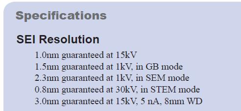
 Name Field Emission Electron Scanning Microscopy (FESEM) Make: JEOL India Pvt Ltd. Model : JEOL JSM 7610f Specification Electron gun : Schottky type field emission (T-FE) gun Electron Beam resolution (secondary
April 10th-12th, 2017
 Thomas LaGrange, Ph.D. Faculty Lecturer and Senior Staff Scientist Introduction: Basics of Transmission Electron Microscopy (TEM) TEM Doctoral Course MS-637 April 10th-12th, 2017 Outline 1. What is microcopy?
PHI 5000 Versaprobe-II Focus X-ray Photo-electron Spectroscopy
 PHI 5000 Versaprobe-II Focus X-ray Photo-electron Spectroscopy The very basic theory of XPS XPS theroy Surface Analysis Ultra High Vacuum (UHV) XPS Theory XPS = X-ray Photo-electron Spectroscopy X-ray
SCANNING ELECTRON MICROSCOPE
 21.05.2010 Hacettepe University SCANNING ELECTRON MICROSCOPE Berrak BOYBEK Tuğba ÖZTÜRK Vicdan PINARBAŞI Cahit YAYAN OUTLINE Definition of scanning electron microscope History Applications of SEM Components
Energy-Filtering. Transmission. Electron Microscopy
 Part 3 Energy-Filtering Transmission Electron Microscopy 92 Energy-Filtering TEM Principle of EFTEM expose specimen to mono-energetic electron radiation inelastic scattering in the specimen poly-energetic