Lab #3 Transparent Conductors
|
|
|
- Nathaniel Sutton
- 5 years ago
- Views:
Transcription
1 Lab #3 Transparent Conductors R.J. Ellingson and M.J. Heben Sept. 23, 2014 PHYS 4580, 6/7280

2 Today at 4:30 pm, R1 Room 1010


Se 2")

3 Impact of Optical Loss in Window Layer in PV Cells O Quantum Efficiency, aka Spectral Response After Cu(InGa)Se 2 Solar Cells, by Shafarman and Stolt, and PVEducation.org
 PV cells R SH = 10,000 Volts (V) Diode equation with R S and")
4 Current density (ma/cm 2 ) Impact of Electrical Loss Due to High Series Resistance (R S ) PV cells R SH = 10,000 Volts (V) Diode equation with R S and R SH :


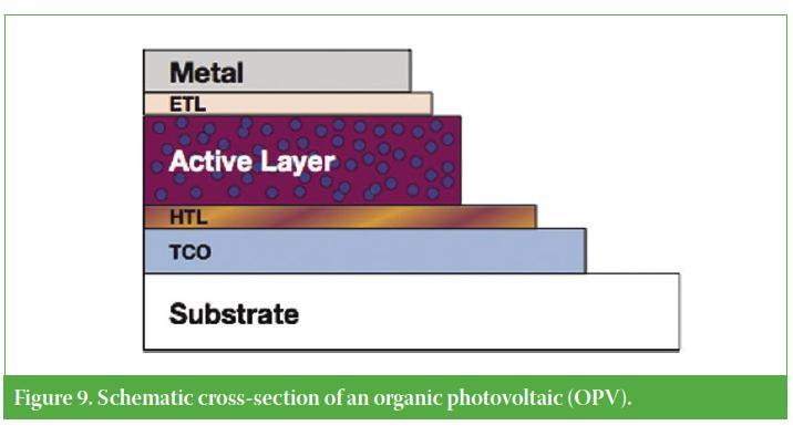
5 TCOs are Used in All PV devices HIT Cell Organic From:
6 Long History of TCO R&D It is an object of this invention to provide on glass or other electrically non-conductive surfaces thin transparent coatings or films possessing the property of electrical conductivity, which coatings are clear, hard and tenacious and of uniform thickness; which are in intimate contact with the glass or other surface; and which will retain these properties under adverse conditions Harold McMaster


7 Monolithically Integrated TF Module The balance between electrical conductivity and optical transparency becomes even more important when current and photons are to be collected over large areas, as is the case in a module. * * Manufacturability is also a big concern!!
8 Typical Reflection, Transmission, and Absorption Data From: Perkins and Ginley
")
+ R(λ)")

9 Total Incident (λ) = A(λ) + T(λ)+ R(λ) Conservation of Energy for each wavelength

10 Defect Equilibria and Doping in TCOs TCO materials are typically wide band gap oxides that are degeneratively doped via defect or substitutional chemistry. The trade off between electrical conductivity and transparency is due to the interplay between the electronic structure of the material and the doping. From: Perkins and Ginley
11 Phase Space for Engineering the Properties of TCOs Additional Parameters for control: Compositional alloys (e.g. Cd 2 SnO 4) Dopants on the anion sublattice (i.e. FTO) Dopants on the cation sublattice (e.g., IT0) Defect equilibria on oxygen subattice New materials Nanomaterials (non-oxides, e.g. singlewall carbon nanotubes, metal nano wires, composites, etc. Conventional compositional space From: Perkins and Ginley


12 ITO Tin doped Indium Oxide UT ITO R Sheet ~ 9 Ω/ Courtesy of A. Phillips In 2 O 3
13 Snell s Law and the Index of Refraction n, the Index of Refraction, aka Refractive Index Describes how light propagates in a medium. Is a dimensionless number. The speed of Iight in a medium is reduced: Where λ 0 is the wavelength in vacuum Although named after Dutch astronomer Willebrord Snellius ( ), the law was first accurately described by the scientist Ibn Sahl at Baghdad court, when in 984 he used the law to derive lens shapes that focus light with no geometric aberrations in the manuscript On Burning Mirrors and Lenses
14 Absorption Up to now, we have considered only the Index of Refraction, n. This is enough when there is no absorption (e.g., wide band gap oxides interacting with sub-band gap light). In general, we must consider refraction, reflection and and absorption, and a complex index: Here, n is still the Index of Refraction, and reflects the phase speed of the light in the medium, but κ now refers to the amount of absorption loss.

15 Typical Reflection, Transmission, and Absorption Data From: Perkins and Ginley

16 Conventional Dual Beam Spectrophotometer In this Lab, we are building a Single Beam Spectrophotometer


17 TCO Coatings on Glass Facilitate High Efficiency window technology Reflection of long wavelength light at night is a big deal! Reduction in Solar Passive Heat gain during the day Consumer s guide to buying energy-efficient windows and doors by Canada s Office of Energy Efficiency Learn about how a Float Line Works at:
 Thin SnO 2 layer (~300 Å) SiO 2 layer (~200 Å) SnO 2 :F layer (~3000 Å) Thick HRT (~850 Å)")
18 TEC Coatings are Complex The TEC-15 glass: Thick soda-lime float glass (3.2 mm) Thin SnO 2 layer (~300 Å) SiO 2 layer (~200 Å) SnO 2 :F layer (~3000 Å) Thick HRT (~850 Å) Courtesy of Prakash Koirala
19 Different kinds of TEC products

20 Thin metal films can also be transparent The sheet resistance values corresponding to the 2, 3.1, 4.5 and 8 nm thick films are 5x10 3, 1.6x10 3, 4x10 2 and 1x10 2 Ω/, respectively.
 image of ~15 nm thick Au deposited by thermal")
21 Sheet Resistance importance of film morphology Scanning Electron Microscope (SEM) image of ~15 nm thick Au deposited by thermal evaporation.
Lab #5 Current/Voltage Curves, Efficiency Measurements and Quantum Efficiency
 Lab #5 Current/Voltage Curves, Efficiency Measurements and Quantum Efficiency R.J. Ellingson and M.J. Heben November 4, 2014 PHYS 4580, 6280, and 7280 Simple solar cell structure The Diode Equation Ideal
Transparent Electrode Applications
 Transparent Electrode Applications LCD Solar Cells Touch Screen Indium Tin Oxide (ITO) Zinc Oxide (ZnO) - High conductivity - High transparency - Resistant to environmental effects - Rare material (Indium)
PHOTOVOLTAICS Fundamentals
 PHOTOVOLTAICS Fundamentals PV FUNDAMENTALS Semiconductor basics pn junction Solar cell operation Design of silicon solar cell SEMICONDUCTOR BASICS Allowed energy bands Valence and conduction band Fermi
Spectroscopic Ellipsometry (SE) in Photovoltaic Applications
 in Photovoltaic Applications") Spectroscopic Ellipsometry (SE) in Photovoltaic Applications Jianing Sun, James Hilfiker, Greg Pribil, and John Woollam c-si PVMC Metrology Workshop July 2012, San Francisco PV key issues Material selection
Spectroscopic Ellipsometry (SE) in Photovoltaic Applications Jianing Sun, James Hilfiker, Greg Pribil, and John Woollam c-si PVMC Metrology Workshop July 2012, San Francisco PV key issues Material selection
Lecture 5 Junction characterisation
 Lecture 5 Junction characterisation Jon Major October 2018 The PV research cycle Make cells Measure cells Despair Repeat 40 1.1% 4.9% Data Current density (ma/cm 2 ) 20 0-20 -1.0-0.5 0.0 0.5 1.0 Voltage
Atmospheric pressure Plasma Enhanced CVD for large area deposition of TiO 2-x electron transport layers for PV. Heather M. Yates
 Atmospheric pressure Plasma Enhanced CVD for large area deposition of TiO 2-x electron transport layers for PV Heather M. Yates Why the interest? Perovskite solar cells have shown considerable promise
Plasmonics. The long wavelength of light ( μm) creates a problem for extending optoelectronics into the nanometer regime.
 creates a problem for extending optoelectronics into the nanometer regime.") Plasmonics The long wavelength of light ( μm) creates a problem for extending optoelectronics into the nanometer regime. A possible way out is the conversion of light into plasmons. They have much shorter
Plasmonics The long wavelength of light ( μm) creates a problem for extending optoelectronics into the nanometer regime. A possible way out is the conversion of light into plasmons. They have much shorter
Optical optimization of perovskite solar cell structure for maximum current collection
 Loughborough University Institutional Repository Optical optimization of perovskite solar cell structure for maximum current collection This item was submitted to Loughborough University's Institutional
THIN FILMS FOR PHOTOVOLTAICS AND OTHER APPLICATIONS. BY Dr.A.K.SAXENA PHOTONICS DIVISION INDIAN INSTITUTE OF ASTROPHYSICS
 THIN FILMS FOR PHOTOVOLTAICS AND OTHER APPLICATIONS BY Dr.A.K.SAXENA PHOTONICS DIVISION INDIAN INSTITUTE OF ASTROPHYSICS BACKGROUND 2.8 meter coating plant at VBO, Kavalur 1.5 meter coating plant at VBO,
NANO TECHNOLOGY IN POLYMER SOLAR CELLS. Mayur Padharia, Hardik Panchal, Keval Shah, *Neha Patni, Shibu.G.Pillai
 NANO TECHNOLOGY IN POLYMER SOLAR CELLS Mayur Padharia, Hardik Panchal, Keval Shah, *Neha Patni, Shibu.G.Pillai Department of Chemical Engineering, Institute of Technology, Nirma University, S. G. Highway,
Electrical Characterisation of TCO thin films (method of four coefficients).
.") Electrical Characterisation of TCO thin films (method of four coefficients). Eric Don, SemiMetrics Ltd. Functional Thin Films 4 th Vacuum Symposium Thursday 17 th October 2013 Agenda TCO Basics TCO Applications
Electrical Characterisation of TCO thin films (method of four coefficients). Eric Don, SemiMetrics Ltd. Functional Thin Films 4 th Vacuum Symposium Thursday 17 th October 2013 Agenda TCO Basics TCO Applications
The Dielectric Function of a Metal ( Jellium )
") The Dielectric Function of a Metal ( Jellium ) Total reflection Plasma frequency p (10 15 Hz range) Why are Metals Shiny? An electric field cannot exist inside a metal, because metal electrons follow the
The Dielectric Function of a Metal ( Jellium ) Total reflection Plasma frequency p (10 15 Hz range) Why are Metals Shiny? An electric field cannot exist inside a metal, because metal electrons follow the
Electrons are shared in covalent bonds between atoms of Si. A bound electron has the lowest energy state.
 Photovoltaics Basic Steps the generation of light-generated carriers; the collection of the light-generated carriers to generate a current; the generation of a large voltage across the solar cell; and
Quantum Dot Technology for Low-Cost Space Power Generation for Smallsats
 SSC06-VI- Quantum Dot Technology for Low-Cost Space Power Generation for Smallsats Theodore G. DR Technologies, Inc. 7740 Kenamar Court, San Diego, CA 92020 (858)677-230 tstern@drtechnologies.com The provision
Chapter 12. Nanometrology. Oxford University Press All rights reserved.
 Chapter 12 Nanometrology Introduction Nanometrology is the science of measurement at the nanoscale level. Figure illustrates where nanoscale stands in relation to a meter and sub divisions of meter. Nanometrology
Chapter 10. Nanometrology. Oxford University Press All rights reserved.
 Chapter 10 Nanometrology Oxford University Press 2013. All rights reserved. 1 Introduction Nanometrology is the science of measurement at the nanoscale level. Figure illustrates where nanoscale stands
Photovoltaic cell and module physics and technology. Vitezslav Benda, Prof Czech Technical University in Prague
 Photovoltaic cell and module physics and technology Vitezslav Benda, Prof Czech Technical University in Prague benda@fel.cvut.cz www.fel.cvut.cz 1 Outlines Photovoltaic Effect Photovoltaic cell structure
Spectroscopic Study of FTO/CdSe (MPA)/ZnO Artificial Atoms Emitting White Color
/ZnO Artificial Atoms Emitting White Color") Spectroscopic Study of FTO/CdSe (MPA)/ZnO Artificial Atoms Emitting White Color Batal MA *, and Alyamani K Department of Physics, College of Science, Aleppo, Syria * Corresponding author: Batal MA, Department
Spectroscopic Study of FTO/CdSe (MPA)/ZnO Artificial Atoms Emitting White Color Batal MA *, and Alyamani K Department of Physics, College of Science, Aleppo, Syria * Corresponding author: Batal MA, Department
2008,, Jan 7 All-Paid US-Japan Winter School on New Functionalities in Glass. Controlling Light with Nonlinear Optical Glasses and Plasmonic Glasses
 2008,, Jan 7 All-Paid US-Japan Winter School on New Functionalities in Glass Photonic Glass Controlling Light with Nonlinear Optical Glasses and Plasmonic Glasses Takumi FUJIWARA Tohoku University Department
Design strategy for Low e windows with effective insulation
 Design strategy for Low e windows with effective insulation Michael P.C. Watts, Impattern Solutions, www.impattern.com Keywords; insulating windows. low emission glass, ABSTRACT Optimal window glass assemblies
Solliance. Perovskite based PV (PSC) Program. TKI Urban Energy Days l e d b y i m e c, E C N a n d T N O
 Program. TKI Urban Energy Days l e d b y i m e c, E C N a n d T N O") Solliance Perovskite based PV (PSC) Program TKI Urban Energy Days - 2017-06-21 l e d b y i m e c, E C N a n d T N O 2 Bringing together research and industry Providing insight and know-how to all partners
Solliance Perovskite based PV (PSC) Program TKI Urban Energy Days - 2017-06-21 l e d b y i m e c, E C N a n d T N O 2 Bringing together research and industry Providing insight and know-how to all partners
Nanocomposite photonic crystal devices
 Nanocomposite photonic crystal devices Xiaoyong Hu, Cuicui Lu, Yulan Fu, Yu Zhu, Yingbo Zhang, Hong Yang, Qihuang Gong Department of Physics, Peking University, Beijing, P. R. China Contents Motivation
Photovoltaic cell and module physics and technology
 Photovoltaic cell and module physics and technology Vitezslav Benda, Prof Czech Technical University in Prague benda@fel.cvut.cz www.fel.cvut.cz 6/21/2012 1 Outlines Photovoltaic Effect Photovoltaic cell
Supporting information for: Semitransparent Polymer-Based Solar Cells with. Aluminum-Doped Zinc Oxide Electrodes
 Supporting information for: Semitransparent Polymer-Based Solar Cells with Aluminum-Doped Zinc Oxide Electrodes Sebastian Wilken,, Verena Wilkens, Dorothea Scheunemann, Regina-Elisabeth Nowak, Karsten
(Co-PIs-Mark Brongersma, Yi Cui, Shanhui Fan) Stanford University. GCEP Research Symposium 2013 Stanford, CA October 9, 2013
 Stanford University. GCEP Research Symposium 2013 Stanford, CA October 9, 2013") High-efficiency thin film nano-structured multi-junction solar James S. cells Harris (PI) (Co-PIs-Mark Brongersma, Yi Cui, Shanhui Fan) Stanford University GCEP Research Symposium 2013 Stanford, CA October
High-efficiency thin film nano-structured multi-junction solar James S. cells Harris (PI) (Co-PIs-Mark Brongersma, Yi Cui, Shanhui Fan) Stanford University GCEP Research Symposium 2013 Stanford, CA October
Cho Fai Jonathan Lau, Xiaofan Deng, Qingshan Ma, Jianghui Zheng, Jae S. Yun, Martin A.
 Supporting Information CsPbIBr 2 Perovskite Solar Cell by Spray Assisted Deposition Cho Fai Jonathan Lau, Xiaofan Deng, Qingshan Ma, Jianghui Zheng, Jae S. Yun, Martin A. Green, Shujuan Huang, Anita W.
Optical Losses of Thin Solar Cells on the Basis of n-zns / p-cdte and n-cds / p-cdte Heterojunctions
 PROCEEDINGS OF THE INTERNATIONAL CONFERENCE NANOMATERIALS: APPLICATIONS AND PROPERTIES Vol. 3 No 4, 04NEA6(5pp) (03) Optical Losses of Thin Solar Cells on the Basis of n-zns / p-cdte and n-cds / p-cdte
X-Ray Interaction with Matter: Absorption, Scattering and Refraction
 X-Ray Interaction with Matter: Absorption, Scattering and Refraction David Attwood University of California, Berkeley 1 The short wavelength region of the electromagnetic spectrum n = 1 δ + iβ δ, β
MEMS Metrology. Prof. Tianhong Cui ME 8254
 MEMS Metrology Prof. Tianhong Cui ME 8254 What is metrology? Metrology It is the science of weights and measures Refers primarily to the measurements of length, weight, time, etc. Mensuration- A branch
DEVICE CHARACTERIZATION OF (AgCu)(InGa)Se 2 SOLAR CELLS
(InGa)Se 2 SOLAR CELLS") DEVICE CHARACTERIZATION OF (AgCu)(InGa)Se 2 SOLAR CELLS William Shafarman 1, Christopher Thompson 1, Jonathan Boyle 1, Gregory Hanket 1, Peter Erslev 2, J. David Cohen 2 1 Institute of Energy Conversion,
DEVICE CHARACTERIZATION OF (AgCu)(InGa)Se 2 SOLAR CELLS William Shafarman 1, Christopher Thompson 1, Jonathan Boyle 1, Gregory Hanket 1, Peter Erslev 2, J. David Cohen 2 1 Institute of Energy Conversion,
Quantum Dots for Advanced Research and Devices
 Quantum Dots for Advanced Research and Devices spectral region from 450 to 630 nm Zero-D Perovskite Emit light at 520 nm ABOUT QUANTUM SOLUTIONS QUANTUM SOLUTIONS company is an expert in the synthesis
PHYSICS nd TERM Outline Notes (continued)
") PHYSICS 2800 2 nd TERM Outline Notes (continued) Section 6. Optical Properties (see also textbook, chapter 15) This section will be concerned with how electromagnetic radiation (visible light, in particular)
PHYSICS 2800 2 nd TERM Outline Notes (continued) Section 6. Optical Properties (see also textbook, chapter 15) This section will be concerned with how electromagnetic radiation (visible light, in particular)
AP5301/ Name the major parts of an optical microscope and state their functions.
 Review Problems on Optical Microscopy AP5301/8301-2015 1. Name the major parts of an optical microscope and state their functions. 2. Compare the focal lengths of two glass converging lenses, one with
Aluminum for nonlinear plasmonics: Methods Section
 Aluminum for nonlinear plasmonics: Methods Section Marta Castro-Lopez, Daan Brinks, Riccardo Sapienza, and Niek F. van Hulst, ICFO - Institut de Ciencies Fotoniques, and ICREA - Institució Catalana de
Charge Extraction. Lecture 9 10/06/2011 MIT Fundamentals of Photovoltaics 2.626/2.627 Fall 2011 Prof. Tonio Buonassisi
 Charge Extraction Lecture 9 10/06/2011 MIT Fundamentals of Photovoltaics 2.626/2.627 Fall 2011 Prof. Tonio Buonassisi 2.626/2.627 Roadmap You Are Here 2.626/2.627: Fundamentals Every photovoltaic device
Direct measurements of exciton diffusion length limitations on organic solar cell performance
 This journal is The Royal Society of Chemistry 212 Supplementary information for Direct measurements of exciton diffusion length limitations on organic solar cell performance Derek R. Kozub, Kiarash Vakhshouri,
UNIT I: Electronic Materials.
 SIDDHARTH INSTITUTE OF ENGINEERING & TECHNOLOGY :: PUTTUR Siddharth Nagar, Narayanavanam Road 517583 QUESTION BANK (DESCRIPTIVE) Subject with Code: SEMICONDUCTOR PHYSICS (18HS0851) Course & Branch: B.Tech
OPTICAL ANALYSIS OF ZnO THIN FILMS USING SPECTROSCOPIC ELLIPSOMETRY AND REFLECTOMETRY.
 OPTICAL ANALYSIS OF ZnO THIN FILMS USING SPECTROSCOPIC ELLIPSOMETRY AND REFLECTOMETRY Katarína Bombarová 1, Juraj Chlpík 1,2, Soňa Flickyngerová 3, Ivan Novotný 3, Július Cirák 1 1 Institute of Nuclear
Plasmonic Hot Hole Generation by Interband Transition in Gold-Polyaniline
 Supplementary Information Plasmonic Hot Hole Generation by Interband Transition in Gold-Polyaniline Tapan Barman, Amreen A. Hussain, Bikash Sharma, Arup R. Pal* Plasma Nanotech Lab, Physical Sciences Division,
Goal for next generation solar cells: Efficiencies greater than Si with low cost (low temperature) processing
 processing") Multi-junction cells MBE growth > 40% efficient Expensive Single crystal Si >20% efficient expensive Thin film cells >10% efficient Less expensive Toxic materials Polymers
Multi-junction cells MBE growth > 40% efficient Expensive Single crystal Si >20% efficient expensive Thin film cells >10% efficient Less expensive Toxic materials Polymers
Low-temperature-processed inorganic perovskite solar cells via solvent engineering with enhanced mass transport
 Electronic Supplementary Material (ESI) for Journal of Materials Chemistry A. This journal is The Royal Society of Chemistry 1 Low-temperature-processed inorganic perovskite solar cells via solvent engineering
26% PK/silicon tandem solar cell with 1 cm 2 area H2020-LCE
 H2020-LCE-205- CHEOPS Production Technology to Achieve Low Cost and Highly Efficient Photovoltaic Perovskite Solar Cells Deliverable WP4 PK/c-Si SHJ tandem device development Author: Arnaud Walter (CSEM)
Plastic Electronics. Joaquim Puigdollers.
 Plastic Electronics Joaquim Puigdollers Joaquim.puigdollers@upc.edu Nobel Prize Chemistry 2000 Origins Technological Interest First products.. MONOCROMATIC PHILIPS Today Future Technological interest Low
Chapter 7. Solar Cell
 Chapter 7 Solar Cell 7.0 Introduction Solar cells are useful for both space and terrestrial application. Solar cells furnish the long duration power supply for satellites. It converts sunlight directly
Real-time and in-line Optical monitoring of Functional Nano-Layer Deposition on Flexible Polymeric Substrates
 Real-time and in-line Optical monitoring of Functional Nano-Layer Deposition on Flexible Polymeric Substrates S. Logothetidis Lab for Thin Films, Nanosystems & Nanometrology, Aristotle University of Thessaloniki,
Astronomy. Optics and Telescopes
 Astronomy A. Dayle Hancock adhancock@wm.edu Small 239 Office hours: MTWR 10-11am Optics and Telescopes - Refraction, lenses and refracting telescopes - Mirrors and reflecting telescopes - Diffraction limit,
SnO2 thin films prepared by APCVD for organic solar cells application
 SnO thin films prepared by APCVD for organic solar cells application D.Hatem, M.S Belkaid, M.Pasquenelli LATAGE Laboratory of Advanced Technologies of Genie Electrics Faculty of Electrical and Computer
The Effects of Hydrazine Monohydrate Surface Doping on Graphene
 Macalester Journal of Physics and Astronomy Volume 4 Issue 1 Spring 2016 Article 8 May 2016 The Effects of Hydrazine Monohydrate Surface Doping on Graphene Christian M. Stewart Macalester College, cstewart@macalester.edu
OPTI510R: Photonics. Khanh Kieu College of Optical Sciences, University of Arizona Meinel building R.626
 OPTI510R: Photonics Khanh Kieu College of Optical Sciences, University of Arizona kkieu@optics.arizona.edu Meinel building R.626 Announcements HW#3 is assigned due Feb. 20 st Mid-term exam Feb 27, 2PM
Uwe Rau Institut für Energieforschung 5 Photovoltaik- Forschungszentrum Jülich GmbH
 Mitglied der Helmholtz-Gemeinschaft Materialforschung für f r DünnschichtphotovoltaikD nnschichtphotovoltaik- Status und neue Entwicklungen Uwe Rau Institut für Energieforschung 5 Photovoltaik- Forschungszentrum
High resolution THz scanning for optimization of dielectric layer opening process on doped Si surfaces
 High resolution THz scanning for optimization of dielectric layer opening process on doped Si surfaces P. Spinelli 1, F.J.K. Danzl 1, D. Deligiannis 1,2, N. Guillevin 1, A.R. Burgers 1, S. Sawallich 3,
Graphene Canada Montreal Oct. 16, 2015 (International Year of Light)
") Luminescence Properties of Graphene A. Beltaos 1,2,3, A. Bergren 1, K. Bosnick 1, N. Pekas 1, A. Matković 4, A. Meldrum 2 1 National Institute for Nanotechnology (NINT), 11421 Saskatchewan Drive, Edmonton,
Luminescence Properties of Graphene A. Beltaos 1,2,3, A. Bergren 1, K. Bosnick 1, N. Pekas 1, A. Matković 4, A. Meldrum 2 1 National Institute for Nanotechnology (NINT), 11421 Saskatchewan Drive, Edmonton,
Optical Systems Program of Studies Version 1.0 April 2012
 Optical Systems Program of Studies Version 1.0 April 2012 Standard1 Essential Understand Optical experimental methodology, data analysis, interpretation, and presentation strategies Essential Understandings:
Nanophysics: Main trends
 Nano-opto-electronics Nanophysics: Main trends Nanomechanics Main issues Light interaction with small structures Molecules Nanoparticles (semiconductor and metallic) Microparticles Photonic crystals Nanoplasmonics
EE 5611 Introduction to Microelectronic Technologies Fall Tuesday, September 23, 2014 Lecture 07
 EE 5611 Introduction to Microelectronic Technologies Fall 2014 Tuesday, September 23, 2014 Lecture 07 1 Introduction to Solar Cells Topics to be covered: Solar cells and sun light Review on semiconductor
Fundamentals of Photovoltaics: C1 Problems. R.Treharne, K. Durose, J. Major, T. Veal, V.
 Fundamentals of Photovoltaics: C1 Problems R.Treharne, K. Durose, J. Major, T. Veal, V. Dhanak @cdtpv November 3, 2015 These problems will be highly relevant to the exam that you will sit very shortly.
Negative Index of Refraction in Optical Metamaterials
 1 Negative Index of Refraction in Optical Metamaterials V. M. Shalaev, W. Cai, U. Chettiar, H.-K. Yuan, A. K. Sarychev, V. P. Drachev, and A. V. Kildishev School of Electrical and Computer Engineering,
Supporting Information
 Electronic Supplementary Material (ESI) for Journal of Materials Chemistry A. This journal is The Royal Society of Chemistry 2018 Supporting Information A minimal non-radiative recombination loss for efficient
Metal nanoparticle-doped coloured films on glass and polycarbonate substrates
 PRAMANA c Indian Academy of Sciences Vol. 65, No. 5 journal of November 2005 physics pp. 931 936 Metal nanoparticle-doped coloured films on glass and polycarbonate substrates S K MEDDA, M MITRA, S DE,
MICROSCOPY COURSE 2012
 MICROSCOPY COURSE 2012 INTRODUCTION TO BASIC LIGHT MICROSCOPY AIM OF THE COURSE Teach basic principles of light microscopy Theoretical background Practical aspects Faced towards applications of light microscopy
Transparent TiO 2 nanotube/nanowire arrays on TCO coated glass substrates: Synthesis and application to solar energy conversion
 Transparent TiO 2 nanotube/nanowire arrays on TCO coated glass substrates: Synthesis and application to solar energy conversion Craig A. Grimes Department of Electrical Engineering Center for Solar Nanomaterials
Chiroptical Spectroscopy
 Chiroptical Spectroscopy Theory and Applications in Organic Chemistry Lecture 2: Polarized light Masters Level Class (181 041) Mondays, 8.15-9.45 am, NC 02/99 Wednesdays, 10.15-11.45 am, NC 02/99 28 Electromagnetic
Physics 208 Final Exam
 Physics 208 Final Exam Name You are graded on your work, with partial credit. See the last pages of the exam for formula sheets. Please be clear and well-organized, so that we can easily follow each step
Calculating Thin Film Stack Properties. Polarization Properties of Thin Films
 Lecture 6: Thin Films Outline 1 Thin Films 2 Calculating Thin Film Stack Properties 3 Polarization Properties of Thin Films 4 Anti-Reflection Coatings 5 Interference Filters Christoph U. Keller, Utrecht
Molecular and Condensed Matter Physics Laboratory (PHYS 4580) Photovoltaic Materials and Device Physics Laboratory (PHYS 6/7280)
 Photovoltaic Materials and Device Physics Laboratory (PHYS 6/7280)") Molecular and Condensed Matter Phsics Laborator (PHYS 4580) Photovoltaic Materials and Device Phsics Laborator (PHYS 6/780) Instructors: Prof. Rand Ellingson, Prof. Mike Heben Teaching Assistant: TBD Course
Molecular and Condensed Matter Phsics Laborator (PHYS 4580) Photovoltaic Materials and Device Phsics Laborator (PHYS 6/780) Instructors: Prof. Rand Ellingson, Prof. Mike Heben Teaching Assistant: TBD Course
Organic Solar Cell: Optics in Smooth and Pyramidal Rough Surface
 IOSR Journal of Electrical and Electronics Engineering (IOSR-JEEE) e-issn: 2278-1676,p-ISSN: 2320-3331, Volume 10, Issue 4 Ver. III (July Aug. 2015), PP 67-72 www.iosrjournals.org Organic Solar Cell: Optics
Superconductivity Induced Transparency
 Superconductivity Induced Transparency Coskun Kocabas In this paper I will discuss the effect of the superconducting phase transition on the optical properties of the superconductors. Firstly I will give
Prentice Hall. Physics: Principles with Applications, Updated 6th Edition (Giancoli) High School
 High School") Prentice Hall Physics: Principles with Applications, Updated 6th Edition (Giancoli) 2009 High School C O R R E L A T E D T O Physics I Students should understand that scientific knowledge is gained from
Prentice Hall Physics: Principles with Applications, Updated 6th Edition (Giancoli) 2009 High School C O R R E L A T E D T O Physics I Students should understand that scientific knowledge is gained from
Nanophotonics: solar and thermal applications
 Nanophotonics: solar and thermal applications Shanhui Fan Ginzton Laboratory and Department of Electrical Engineering Stanford University http://www.stanford.edu/~shanhui Nanophotonic Structures Photonic
Organic LEDs part 6. Exciton Recombination Region in Organic LEDs. Handout: Bulovic, et al., Chem. Phys. Lett. 287, 455 (1998); 308, 317 (1999).
; 308, 317 (1999).") Organic LEDs part 6 Exciton Recombination Region in Organic LEDs White OLED Flexible OLEDs Solvation Effect Solid State Solvation Handout: Bulovic, et al., Chem. Phys. Lett. 287, 455 (1998); 308, 317 (1999).
Organic LEDs part 6 Exciton Recombination Region in Organic LEDs White OLED Flexible OLEDs Solvation Effect Solid State Solvation Handout: Bulovic, et al., Chem. Phys. Lett. 287, 455 (1998); 308, 317 (1999).
SURFACE PLASMONS AND THEIR APPLICATIONS IN ELECTRO-OPTICAL DEVICES
 SURFACE PLASMONS AND THEIR APPLICATIONS IN ELECTRO-OPTICAL DEVICES Igor Zozouleno Solid State Electronics Department of Science and Technology Linöping University Sweden igozo@itn.liu.se http://www.itn.liu.se/meso-phot
Supporting Information. Monolithic perovskite-homojunction silicon tandem solar cell with over 22% efficiency
 Electronic Supplementary Material (ESI) for Energy & Environmental Science. This journal is The Royal Society of Chemistry 2017 Electronic Supplementary Information (ESI) for Energy & Environmental Science
e - Galvanic Cell 1. Voltage Sources 1.1 Polymer Electrolyte Membrane (PEM) Fuel Cell
 Fuel Cell") Galvanic cells convert different forms of energy (chemical fuel, sunlight, mechanical pressure, etc.) into electrical energy and heat. In this lecture, we are interested in some examples of galvanic cells.
Galvanic cells convert different forms of energy (chemical fuel, sunlight, mechanical pressure, etc.) into electrical energy and heat. In this lecture, we are interested in some examples of galvanic cells.
CIGS und Perowskit Solarzellenforschung an der Empa
 CIGS und Perowskit Solarzellenforschung an der Empa Dr. Stephan Buecheler Contact: stephan.buecheler@empa.ch Direct: +4158 765 61 07 Laboratory for Thin Films and Photovoltaics, Empa - Swiss Federal Laboratories
University of South Florida Development of a Smart Window for Green Buildings in Florida
 University of South Florida Development of a Smart Window for Green Buildings in Florida PI: Dr. Sarath Witanachchi Students: Marak Merlak, Ph.D Description: This proposal is aimed at developing a smart
Ultra-Slow Light Propagation in Room Temperature Solids. Robert W. Boyd
 Ultra-Slow Light Propagation in Room Temperature Solids Robert W. Boyd The Institute of Optics and Department of Physics and Astronomy University of Rochester, Rochester, NY USA http://www.optics.rochester.edu
Cathodolumiescence Studies of the Density of States of Disordered Silicon Dioxide
 Utah State University DigitalCommons@USU Presentations Materials Physics Fall 2014 Cathodolumiescence Studies of the Density of States of Disordered Silicon Dioxide JR Dennison Utah State Univesity Amberly
-I (PH 6151) UNIT-V PHOTONICS AND FIBRE OPTICS
 UNIT-V PHOTONICS AND FIBRE OPTICS") Engineering Physics -I (PH 6151) UNIT-V PHOTONICS AND FIBRE OPTICS Syllabus: Lasers Spontaneous and stimulated emission Population Inversion -Einstein s co-efficient (Derivation)- types of lasers-nd-yag,co
Engineering Physics -I (PH 6151) UNIT-V PHOTONICS AND FIBRE OPTICS Syllabus: Lasers Spontaneous and stimulated emission Population Inversion -Einstein s co-efficient (Derivation)- types of lasers-nd-yag,co
Spiro-Configured Bifluorenes: Highly Efficient Emitter for UV Organic Light-Emitting Device and Host Material for Red Electrophosphorescence
 Spiro-Configured Bifluorenes: Highly Efficient Emitter for UV Organic Light-Emitting Device and Host Material for Red Electrophosphorescence Ken-Tsung Wong,* a Yuan-Li Liao, a Yu-Ting Lin, b Hai-Ching
COMSOL Multiphysics Software and Photovoltaics: A Unified Platform for Numerical Simulation of Solar Cells and Modules
 COMSOL Multiphysics Software and Photovoltaics: A Unified Platform for Numerical Simulation of Solar Cells and Modules Marco Nardone, Ph.D. Bowling Green State University Bowling Green, Ohio 1 Photovoltaics
TEACHERS OF SCIENCE: Physics 9-12 FORM I-D GRID
 8710.4750 TEACHERS OF SCIENCE: sics 9-12 FORM I-D GRID Professional Education Program Evaluation Report (PEPER II) 8710.4750 Teachers of Science: sics 9-12 Subp. 7. Subject matter standards for teachers
A) n 1 > n 2 > n 3 B) n 1 > n 3 > n 2 C) n 2 > n 1 > n 3 D) n 2 > n 3 > n 1 E) n 3 > n 1 > n 2
 n 1 > n 2 > n 3 B) n 1 > n 3 > n 2 C) n 2 > n 1 > n 3 D) n 2 > n 3 > n 1 E) n 3 > n 1 > n 2") 55) The diagram shows the path of a light ray in three different materials. The index of refraction for each material is shown in the upper right portion of the material. What is the correct order for
55) The diagram shows the path of a light ray in three different materials. The index of refraction for each material is shown in the upper right portion of the material. What is the correct order for
Question 1. (Marks 16)
") 5 Question 1. (Marks 16) Consider the circuit shown in the figure, where C 1 = 6.00µF, C 2 = 3.00µF, and V = 20.0V. Capacitor C 1 is first charged by closing switch S 1. Switch S 1 is then opened, and
5 Question 1. (Marks 16) Consider the circuit shown in the figure, where C 1 = 6.00µF, C 2 = 3.00µF, and V = 20.0V. Capacitor C 1 is first charged by closing switch S 1. Switch S 1 is then opened, and
Imaging Methods: Scanning Force Microscopy (SFM / AFM)
") Imaging Methods: Scanning Force Microscopy (SFM / AFM) The atomic force microscope (AFM) probes the surface of a sample with a sharp tip, a couple of microns long and often less than 100 Å in diameter.
Imaging Methods: Scanning Force Microscopy (SFM / AFM) The atomic force microscope (AFM) probes the surface of a sample with a sharp tip, a couple of microns long and often less than 100 Å in diameter.
Graded S i N x /S i O x N y Layers as Antireflective Coatings for Solar Cells Based on GaAs and Silicon Crystalline
 Science Research 2016; 4(1): 21-25 Published online February 25, 2016 (http://www.sciencepublishinggroup.com/j/sr) doi: 10.11648/j.sr.20160401.14 ISSN: 2329-0935 (Print); ISSN: 2329-0927 (Online) Graded
LC circuit: Energy stored. This lecture reviews some but not all of the material that will be on the final exam that covers in Chapters
 Disclaimer: Chapter 29 Alternating-Current Circuits (1) This lecture reviews some but not all of the material that will be on the final exam that covers in Chapters 29-33. LC circuit: Energy stored LC
Calculating Thin Film Stack Properties
 Lecture 5: Thin Films Outline 1 Thin Films 2 Calculating Thin Film Stack Properties 3 Fabry-Perot Tunable Filter 4 Anti-Reflection Coatings 5 Interference Filters Christoph U. Keller, Leiden University,
Whisker growth on Sn thin film accelerated under gamma-ray induced electric field
 Whisker growth on Sn thin film accelerated under gamma-ray induced electric field Diana Shvydka, 1 Morgan Killefer, 2 Vamsi Borra, 3 Daniel G. Georgiev, 3 Victor G. Karpov, 2 E. Ishmael Parsai 1 1 Dept.
YOUR NAME Sample Final Physics 1404 (Dr. Huang)), Correct answers are underlined.
), Correct answers are underlined.") YOUR NAME Sample Final Physics 1404 (Dr. Huang)), Correct answers are underlined. Useful constants: e=1.6 10-19 C, m e =9.1 10-31 kg, m p =1.67 10-27 kg, ε 0 =8.85 10-12 C 2 /N m 2, c=3 10 8 m/s k e =8.99
YOUR NAME Sample Final Physics 1404 (Dr. Huang)), Correct answers are underlined. Useful constants: e=1.6 10-19 C, m e =9.1 10-31 kg, m p =1.67 10-27 kg, ε 0 =8.85 10-12 C 2 /N m 2, c=3 10 8 m/s k e =8.99
LECTURE 11 ELECTROMAGNETIC WAVES & POLARIZATION. Instructor: Kazumi Tolich
 LECTURE 11 ELECTROMAGNETIC WAVES & POLARIZATION Instructor: Kazumi Tolich Lecture 11 2 25.5 Electromagnetic waves Induced fields Properties of electromagnetic waves Polarization Energy of electromagnetic
Supplementary information
 Supplementary information Neutral Colour Semitransparent Microstructured Perovskite Solar Cells Giles E. Eperon, Victor M. Burlakov, Alain Goriely and Henry J. Snaith 1. Controlling dewetting to achieve
PHYS 4400, Principles and Varieties of Solar Energy Instructor: Randy J. Ellingson The University of Toledo
 Light and Photons PHYS 4400, Principles and Varieties of Solar Energy Instructor: Randy J. Ellingson The University of Toledo January 16, 2014 Light What is light? Electromagnetic wave direction of the
LECTURE 11 ELECTROMAGNETIC WAVES & POLARIZATION. Instructor: Kazumi Tolich
 LECTURE 11 ELECTROMAGNETIC WAVES & POLARIZATION Instructor: Kazumi Tolich Lecture 11 2 25.5 Electromagnetic waves Induced fields Properties of electromagnetic waves Polarization Energy of electromagnetic
FACULTY OF ENGINEERING ALEXANDRIA UNVERSITY. Solid State lab. Instructors Dr. M. Ismail El-Banna Dr. Mohamed A. El-Shimy TA Noha Hanafy
 FACULTY OF ENGINEERING ALEXANDRIA UNVERSITY Solid State lab Instructors Dr. M. Ismail El-Banna Dr. Mohamed A. El-Shimy TA Noha Hanafy 2017-2018 first term A. Experiments 1- Relationship between the intensity
MSE 321 Structural Characterization
 Optical Microscope Plan Lenses In an "ideal" single-element lens system all planar wave fronts are focused to a point at distance f from the lens; therefore: Image near the optical axis will be in perfect
Session V: Graphene. Matteo Bruna CAMBRIDGE UNIVERSITY DEPARTMENT OF ENGINEERING
 Session V: Graphene Matteo Bruna Graphene: Material in the Flatland Graphite Graphene Properties: Thinnest imaginable material Good(and tunable) electrical conductor Strongest ever measured Stiffest known
Atomic Layer Deposition of Chalcogenide Thin Films
 Atomic Layer Deposition of Chalcogenide Thin Films PUBLICATION REVIEW ON ULTRATECH ALD SYSTEMS 09.10.2015 1 Highlights Benefits of ALD for nano-manufacturing of chalcogenides Atomic level thickness control
Chapter Ray Optics and Optical Instrument
 Chapter Ray Optics and Optical Instrument Q1. Focal length of a convex lens of refractive index 1.5 is 2 cm. Focal length of the lens when immersed in a liquid of refractive index of 1.25 will be [1988]
February 1, 2011 The University of Toledo, Department of Physics and Astronomy SSARE, PVIC
 FUNDAMENTAL PROPERTIES OF SOLAR CELLS February 1, 2011 The University of Toledo, Department of Physics and Astronomy SSARE, PVIC Principles and Varieties of Solar Energy (PHYS 4400) and Fundamentals of
Patterning of ITO Layer on Glass with High Repetition Rate Picosecond Lasers
 JLMN-Journal of Laser Micro/Nanoengineering Vol., No., 7 Patterning of ITO Layer on Glass with High Repetition Rate Picosecond Lasers Gediminas RAČIUKAITIS, Marijus BRIKAS, Mindaugas GEDVILAS and Gediminas