Polarization Control of Electron Tunneling into Ferroelectric Surfaces
|
|
|
- Marcus Jackson
- 5 years ago
- Views:
Transcription
1 Submitted: Science Date: 01/20/2009 Revised: 05/07/2009 Polarization Control of Electron Tunneling into Ferroelectric Surfaces Peter Maksymovych* 1, Stephen Jesse 1, Pu Yu 2, Ramamoorthy Ramesh 2, Arthur P. Baddorf 1, and Sergei V. Kalinin 1 1 Center for Nanophase Materials Science, Oak Ridge National Laboratory, Oak Ridge, TN, Department of Materials Science and Engineering and Department of Physics, University of California, Berkeley, CA *corresponding author: maksymovychp@ornl.gov 1
2 Description Switchable polarization of a thin film perovskite oxide controls the tunneling conductance of a nanoscale metal-ferroelectric junction by several orders of magnitude, enabling new approaches to high density non-volatile memory. Abstract We demonstrate a highly reproducible control of local electron transport through a ferroelectric oxide via its spontaneous polarization. Electrons are injected from the tip of an atomic force microscope into a thin film of lead-zirconate titanate, (Pb(Zr 0.2 Ti 0.8 )O 3, in the regime of electron tunneling assisted by a high electric field (Fowler-Nordheim tunneling). The tunneling current exhibits a pronounced hysteresis with abrupt switching events that coincide, within experimental resolution, with the local switching of ferroelectric polarization. The large spontaneous polarization of the PZT film results in 100-fold amplification of the tunneling current upon ferroelectric switching. The magnitude of the effect is subject to electrostatic control via ferroelectric switching, suggesting possible applications in ultra-high density data storage and spintronics. In quantum mechanics, a particle can tunnel through a potential barrier that exceeds the particle s energy. Tunneling underlies the operation of the resonant tunneling diode (1) and flashmemory (2), enables atomically resolved imaging in scanning tunneling microscopy (3) and holds promise for quantum computing based on SQUID magnetometers and quantum dots (4, 5). Replacing a conventional insulator in the tunnel junction with electronically correlated materials can 2
3 modify existing devices and yield new types of electronic functionality. In one of the earliest such concepts proposed by Esaki (6), dubbed a polar switch, the tunneling barrier was composed of a ferroelectric oxide, which would have spontaneous, non-volatile polarization that could be switched in direction with an applied electric field. In a number of recent theoretical papers (7-9), including first-principles studies, the spontaneous polarization was predicted to modulate the height of the tunneling barrier, which would yield distinct nonvolatile conductance states that could subsequently be used to encode information. The density of the recorded information can potentially approach near-atomic limit, since the width of polarization domains in nanoscale ferroelectric oxides can be as small as several nanometers (10, 11). It has proven difficult to find a material system that would simultaneously satisfy the dimensional constraints for tunneling and ferroelectricity. Ferroelectricity vanishes below a critical thickness, varying from 1 to 10 nanometers (12, 13), whereas direct tunneling is only feasible across a wide band-gap oxide thinner than ~2 nm. Although the polar distortion in perovskite oxides leading to ferroelectricity was recently reported even in three unit-cell (~1.2 nm) films (11), the presence of switchable polarization at this ultrathin limit has not yet been confirmed. Switching could be hindered by the formation of lamellar domain structures and a strong preference of the polarization to remain in the as-grown state (14). Gajek et al. (15) have recently demonstrated hysteresis of tunneling conductance through a 2-nm multiferroic film, albeit with a very small magnitude of <15%, as expected for the diminishing spontaneous polarization in such thin films (12). In addition to these fundamental physical constraints, the defect-rich nature of transition metal oxides often favors filamentary and defect-mediated conduction mechanisms over intrinsic tunneling (16, 17). 3
4 To demonstrate the polarization control of electron transport through a ferroelectric oxide, we used the tunneling barrier electronically defined at the junction between a sharp metal tip and the ferroelectric surface. We could thus avoid the necessity to reduce the oxide width, and work with relatively thick ferroelectric films (30 nm) with large spontaneous polarization. The electrons were injected into the oxide from the metal tip in the regime of Fowler-Nordheim (FN) tunneling (18) across an effectively triangular-shaped barrier. The FN-conductance was found to be strongly dependent on the polarization direction, which resulted in abrupt enhancement of current (up to 500- fold) at ferroelectric switching events. We have studied the local transport properties of the (100)-oriented 30-nm ferroelectric film of tetragonal Pb(Zr 0.2 Ti 0.8 )O 3 (PZT) using atomic force microscopy (AFM) in ultrahigh vacuum (UHV). The surface of the film was flat and had well-defined unit-cell steps (Fig. 1A). The preferred direction of spontaneous polarization is toward the bottom metallic La 0.7 Sr 0.3 MnO 3 (LSMO) electrode. The polarization could be readily switched in UHV, Fig. 1B, by biasing the AFM tip relative to the bottom electrode. The switching bias, determined from the piezoresponse hysteresis loops (19), varied across the surface because of the inherent disorder in the film with the averages of 1.3±0.6 V and -3.7±0.8 V for the positive and negative nucleation bias, respectively (Fig. 1C). The hysteresis loops also revealed a significant built-in potential across the film (~ 1.2 V). Local current-voltage (I-V) characteristics (Fig. 1D) were highly rectifying with no current above the noise-floor (~ 40 pa) observed at positive tip bias. The shape of the I-V curve, however, depended strongly on the probed range of the tip bias. The onset of current was smooth, and the I-V curve exhibited little or no hysteresis between forward (increasing negative tip bias) and backward bias ramps if the positive bias was limited to < 0 V. In contrast, increasing the upper limit to >2 V yielded an abrupt current jump in the forward direction, followed by a continuous region and a 4
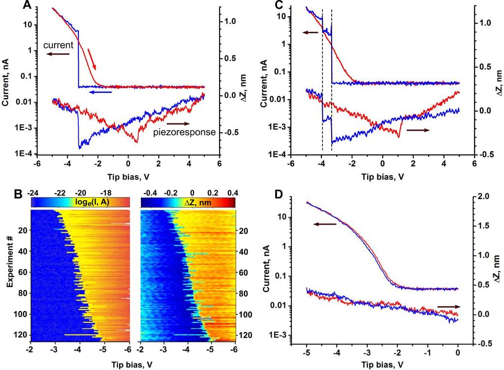
5 smooth reverse curve, Fig. 1E. The tip bias at the current discontinuity varied across the surface with an average value of -3.3±1.1 V. Because this voltage variation is well within the range of ferroelectric switching, (Fig. 1C), the observed current hysteresis may be related to the ferroelectric polarization of the surface. However, a rigorous correlation can be established only in a simultaneous measurement of the ferroelectric and conducting properties, because transition metal oxides can exhibit defect-mediated resistive switching (16, 20, 21) and charge injection from the AFM tip was previously shown to induce local conducting states in lead-zirconate films (22). To acquire the local piezoresponse hysteresis loops (Fig. 1B), we applied an AC-bias to the AFM tip after subsequent DC-poling cycles (19). A typical AC-bias amplitude of > 0.5 V tended to smooth the observed ferroelectric switching event, and also interfered with the conductance measurements. Thus, we acquired local strain loops via a static displacement of the AFM tip during the DC-bias ramp (23). As seen in Fig. 2A, the strain loop in a symmetric bias window (+5 V to - 5V) had a clear butterfly shape. The surface locally expanded (contracted) upon increasing bias until a ferroelectric switching event changed the deformation direction to compression (expansion). The statistical distributions of the switching bias from the strain and AC-piezoresponse measurements were similar, Fig. 3A, although the former yielded slightly smaller average values. This difference was likely caused by a relaxation effect, in that the occurrence of a stable reverse-polarity domain was detected at zero tip bias in the AC-technique and a non-zero value in the strain-loop measurements. The discontinuities in the strain loop and the simultaneously acquired current hysteresis coincide at negative tip bias (Fig. 2A). This behavior was reproduced in all of ~ 600 hysteretic I-V curves acquired in different places on the PZT surface, a subset of which is shown in Fig. 2B. In about 10% of the hysteretic I-V curves, several discontinuities were observed that also displayed a 5
6 similar pattern of piezoelectric displacements (Fig. 2C). This response may be indicative of defectmediated pinning of the reversed-polarization domain growth. At the same time, smooth I-V curves correlated only with continuous strain loops, where no ferroelectric switching occurs (Fig. 2D). Finally, the transition between smooth (Fig. 2D) and hysteretic I-V characteristics (Fig. 2A) occurs at the minimal positive bias required to open the butterfly-shaped strain loop (Fig. S1). These measurements rigorously establish the correlation between switching of ferroelectric polarization and electronic conductance. To rule out a possible involvement of residual adsorbates in the observed effects, we carried out a control experiment on a similarly grown 50 nm PZT/LSMO film, finding that annealing the film in 20 mtorr oxygen atmosphere at T = 600 K for 20 minutes had no observable effect on the polarization-dependent electron transport through the film (Fig. S2). We would like to add that the reproducibility of I-V curves across the surface distinguishes our results from those of filamentary conduction, because the spatial distribution of conducting filaments was shown to be very non-uniform (17). Also, highly rectifying I-V characteristics (Fig. 2A,C) are distinct from a previous study of a macroscopic ferroelectric capacitor, where the I-V curves became Ohmic after polarization switching (24). Smooth I-V curves can be linearized in the coordinates log(i/v 2 ) = f(v -1 ), which is a signature of Fowler-Nordheim tunneling through a triangular potential barrier. The FN-tunneling current (18), I A eff 3 e mpt E 8 hm PZT B 2 8 2m exp( 3he PZT 3 / 2 B, (1) ) E is a function of the barrier height, electric field, E, effective tunneling area, A B eff, and the effective electron mass in the tip (m Pt, assumed ~ m e ) and PZT (m PZT, assumed here ~3m e ). The observed current hysteresis implies that the FN-tunneling conductance is drastically reduced when the 6
7 polarization vector is anti-parallel to the applied electric field. Polarization switching is accompanied by changes in the local strain and electrostatics in the material, both of which can be the source of hysteresis. We can rule out the nanomechanical origins, such as the local expansion of the material and the change of the tip-surface contact area A eff. Indeed, this piezoelectric effect would increase the width of the tunneling barrier upon switching (7), leading to a drop in the tunneling conductance, opposite to the observed trend (Fig. 2A-C). The changes in the tip-surface contact area were ascertained to be insignificant by measuring the bias-dependence of the contact resonance of the cantilever (Fig. 3B). The frequency varied by only ~300 Hz across the whole bias range, corresponding to at most a twofold change in the contact area (25).The current, however, increased by several orders of magnitude upon switching. Furthermore, the resonance frequency decreased at negative tip bias indicating that the contact area slightly decreases too. The FN-current hysteresis must therefore arise from electrostatic effects, originating from the screening of the bound polarization charge on ferroelectric surfaces (7, 9). The barrier height in Eq. 1 corresponds to the height of the Schottky barrier at the metalferroelectric interface. The interfacial band alignment is influenced by the presence of bound dipoles (26). These dipoles may originate from dangling bonds or polar terminations in conventional semiconductors, whereas in ferroelectrics there is an additional strong component caused by the bound polarization charge. In the simplest one dimensional model, the metal and ferroelectric are separated by an ultrathin insulating layer that could arise from a non-epitaxial contact (between the tip and the surface in our case), the reacted surface layer, or the formation of an intrinsic dielectric dead-layer (27). The potential drop across the insulating layer rigidly shifts the electronic bands of the ferroelectric relative to the Fermi level of the tip (Fig. 3C). The change of the barrier height can 7
8 be estimated as e I B S I (26), where I is the width of the dielectric gap, I its dielectric constant and s is the surface charge density. The magnitude of s is determined by the competition between internal and external screening of the polarization charge, as well as a possible suppression of the polarization charge in the vicinity of the interface (27). B is ~0.7 ev for an estimated I = 0.06 nm, I = 0 and s = 0.1 C/m 2. This difference is large enough to fully suppress FN electron tunneling into an oppositely polarized film, as observed experimentally. Because the accumulation of positive surface charge on an upward polarized surface will shift the ferroelectric bands down in energy (Fig. 3C), the Schottky barrier for electron tunneling into the conduction band of the ferroelectric (n-type band alignment) will decrease in height. The n-type band alignment in the tip-surface junction is consistent with the observation of current at negative tip polarity. Therefore the external screening model predicts the right sign of the effect irrespectively of the detailed mechanisms. Our estimate also agrees with recent ab-initio calculations of an epitaxial SrRuO 3 /BaTiO 3 /SrRuO 3 capacitor, where the barrier height decreases by ~0.4 ev for upward polarization due to combined effects of electrostatics and local chemical bonding (9). Fitting of Eq. 1 to the experimental I-V curves with the assumption of a 300 nm 2 contact area (20 nm tip diameter) reveals that the electric field has to exceed 5 MV/cm to allow tunneling across a realistic potential barrier of ev between Pt and PZT (28). This value is at least five times higher than what would be achieved if the potential drop were uniform across the PZT film. The required non-uniformity can be produced by the sharpness of the metal tip producing a localized electric field in the vicinity of the surface, or by a relatively large total density of deep and shallow levels in the band-gap of the ferroelectric that yield narrow Schottky barriers via effective screening. 8
9 To assess the strength of a localized field, we have modeled the tip-surface junction as a disk in contact with a dielectric surface (29). Although the model fits the data very well (Fig. 3D), sufficiently localized fields in a dielectric substrate (or a fully depleted film) are produced if the tipdiameter is less than 5 nm (25), while the effective tunneling area is ~ 4 nm 2. These values are less than the expected tip diameter of >20 nm in contact-mode AFM. Thus, the localized field enhancement can take place if there is a sharp asperity on the tip surface that dominates the tunneling transport. Notably, although the potential drop across the film is non-uniform, it is almost identically linear several nanometers under the tip (Fig. S4), creating a narrow triangular potential barrier where the FN-tunneling equation applies. The second possibility of thin Schottky barriers was previously invoked to rationalize the occurrence of Fowler-Nordheim tunneling in capacitor experiments with macroscopic electrodes (30, 31). Several works (30, 32) have reported a relatively high total density of rechargeable levels in Pb(Zr 0.2 Ti 0.8 )O 3 films, up to cm -3. The ferroelectric film can then be treated as a doped semiconductor, where the polarization charge is screened by charged and ionized defects (33). The depletion width and the corresponding maximum electric field (E m ) at the interface become polarization dependent. E m can exceed 4 MV/cm already at a tip-bias of 2 V (25). Substituting the bias dependent E m into the Eq. (1) also yields a good fit to the measured I-V curves (Fig. 3D), with an average barrier height of 1.1±0.1 ev, a realistic tunneling area of 300±6 nm 2 (tip diameter ~ 20 nm) and a spontaneous polarization of 0.4±0.1 C/cm 2. The depletion width in this model is polarization dependent, which will introduce strong current hysteresis in addition to that from the change of the barrier height. Although we cannot determine which of the above models is dominant, we have observed similar local transport through 50 nm PZT films (Fig. S2) and 5 nm BiFeO 3 films (Fig. S3). The 9
10 barrier narrowing thus appears to be an intrinsic property of high-field transport in perovskite ferroelectrics, in agreement with a number of capacitor measurements (30). The polarizationdependence of the Schottky barrier height will have an equally pronounced effect on local conductance independently of the model, and it will also produce strong conductance hysteresis in the Schottky emission (34), another interface-limited conduction mechanism that exhibits exponential dependence on the barrier height. The pronounced coupling between ferroelectricity and FN tunneling results in high-to-low conductance ratios up to 500:1 in the region of the current hysteresis, Fig. 4A. The conductance ratio grows exponentially with decreasing ferroelectric switching voltage, because the downwardpolarized surface shows no conductance up to the switching voltage (Fig. 1C,D). The hysteresis observed in our measurements was already sufficient to demonstrate a prototype resistive memory action. Fig. 4B shows a series of consecutive write (+/- 5V) and read (- 2V) bias pulses, where the read voltage was chosen to yield measurable current on the upward-polarized surface. The memory effect is manifested in the ability to read-out the high (30-50 pa) and low (noise-limited to ~1 pa) conductance states, and to do so non-destructively (Fig. 4B) because the read bias was at least 1 V below the onset of ferroelectric switching. Theoretically, FN-conductance ratio can exceed five orders of magnitude, depending on the polarization-induced change of the barrier height, tip bias, size and material properties (Fig. S6). The hysteresis window can be optimized through the built-in field across the ferroelectric film, by varying its dimensions, doping and the choice of the bottom electrode and tip materials. This is exemplified in Fig. 4C,D for 50 nm PZT films grown on SrRuO 3 (SRO) and La 0.7 Sr 0.3 MnO 3 electrodes. The I-V curve on the PZT/SRO film revealed negligible hysteresis, because ferroelectric switching occurred in the bias-range where the film was insulating, Fig. 4C. Substituting SRO with LSMO produced strong built-in field, overlapping the bias range of 10
11 conductance and polarization switching events and creating a very pronounced conductance hysteresis, Fig. 4D. The large magnitude of the conductance hysteresis, its tunability via ferroelectric switching and the ability to implement non-destructive resistive (rather than capacitive) read-out of polarization direction indicate the promise of ferroelectric Fowler-Nordheim tunneling in the development of ultra-high density information storage. According to a recent theoretical study, the minimum recordable domain size decreases with thickness, but passes through a minimum, increasing again for the thinnest films (35). A relatively weak thickness dependence of FN-tunneling will thus be critical in achieving the highest density of resistively readable information on a ferroelectric surface. The compatibility of FN tunneling with multiferroic oxides (such as BiFeO 3 ) also poses a possibility of implementing multiferroic control of this transport regime for spintronic applications. Finally, polarization-dependent transport can be used to study the ferroelectric property itself, in an attempt to reveal the switching mechanisms in nanoscale systems and explore the role of defects. References 1. R. Tsu, L. Esaki, Appl. Phys. Lett. 22, 562 (1973). 2. R. Bez, E. Camerlenghi, A. Modelli, A. Visconti, Proceedings of the IEEE 91, 489 (2003). 3. G. Binnig, H. Rohrer, IBM J. Res. Develop. 30, 4 (1986). 4. J. Majer et al., Nature 449, 443 (2007). 5. J. M. Elzerman et al., Nature 430, 431 (2004). 6. L. Esaki, R. B. Laibowitz, P. J. Stiles, IBM Tech. Discl. Bull. 13, 2161 (1971). 7. H. Kohlstedt, N. A. Pertsev, J. R. Contreras, R. Waser, Phys. Rev. B 72, (2005). 8. E. Y. Tsymbal, H. Kohlstedt, Science 313, 181 (2006). 9. J. P. Velev et al., Nano Lett. 9, 427 (2009). 10. P. Aguado-Puente, J. Junquera, Phys. Rev. Lett. 100, (2008). 11. D. D. Fong et al., Science 304, 1650 (2004). 12. J. Junquera, P. Ghosez, Nature 422, 506 (2003). 11
12 13. C. H. Ahn, K. M. Rabe, J.-M. Triscone, Science 303, 488 (2004). 14. V. Nagarajan et al., J. Appl. Phys. 100, (2006). 15. M. Gajek et al., Nat. Mat. 6, 296 (2007). 16. H. Kohlstedt et al., Appl. Phys. Lett. 92, (2008). 17. K. Szot, W. Speier, G. Bihlmayer, R. Waser, Nat. Mat. 5, 312 (2006). 18. R. H. Fowler, L. W. Nordheim, Proc. Roy. Soc. A 119, 173 (1928). 19. S. Jesse et al., Nat. Mat. 7, 209 (2008). 20. R. Waser, M. Aono, Nat. Mat. 6, 833 (2007). 21. Y. Watanabe, Ferroelectrics 349, 190 (2007). 22. C. Yoshida, A. Yoshida, H. Tamura, Appl. Phys. Lett. 75, 1449 (1999). 23. S. Wicks, V. Anbusathiah, V. Nagarajan, Nanotechnology 18, (2007). 24. P. W. M. Blom, R. M. Wolf, J. F. M. Cillessen, M. P. C. M. Krijn, Phys. Rev. Lett. 73, 2107 (1994). 25. Supporting material available on Science Online. 26. R. T. Tung, Phys. Rev. B 64, (2001). 27. A. K. Taganstev, G. Gerra, J. Appl. Phys. 100, (2006). 28. I. Stolichnov, A. Tagantsev, N. Setter, J. S. Cross, M. Tsukada, Appl. Phys. Lett. 75, 1790 (1999). 29. A. N. Morozovska, S. V. Kalinin, E. A. Eliseev, S. V. Svechnikov, Ferroelectrics 354, 198 (2007). 30. J. F. Scott, Ferroelectric Memories (Springer, 2000). 31. I. Stolichnov, A. K. Taganstev, E. L. Colla, N. Setter, Appl. Phys. Lett. 73, 1361 (1998). 32. L. Pintilie et al., J. Appl. Phys. 98, (2005). 33. L. Pintilie, M. Alexe, J. App. Phys. 98, (2005). 34. S. M. Sze, Semiconductor Devices: Physics and Technology, 2nd Ed. (Wiley, 2001). 35. A. N. Morozovska, E. A. Eliseev, Phys. B - Cond. Mat. 373, 54 (2006). 36. S. Jesse, A. P. Baddorf, S. V. Kalinin, Nanotechnology 17, 1615 (2006). 37. Experiments were done at the Center for Nanophase Materials Sciences, Office of Basic Energy Sciences, U.S. Department of Energy. PM: Research performed as a Eugene P. Wigner Fellow and staff member at the Oak Ridge National Laboratory. The work at Berkeley is partially supported by the SRC-NRI-WINS program as well as by the Director, Office of Science, Office of Basic Energy Sciences, Materials Sciences Division of the U. S. Department of Energy under contract No. DE-AC02-05CH
13 Figure captions Figure 1. (A) Top-to-bottom: the surface topography of the PZT film imaged in the contact-mode; simultaneously acquired piezoresponse amplitude, revealing domains of upward ( ) and downward ( ) polarization (locally recorded by scanning a biased AFM tip) separated by a domain wall (black line); topographic profile along the red dashed line. (B) Fourty piezoresponse hysteresis loops taken at random locations on the surface of the PZT sample. Schematics show domain structures forming under the tip on the positive and negative branches of the hysteresis curves. (C) Distribution of the positive (red) and negative (blue) switching biases, measured at 3% of the total piezoresponse in the hysteresis loop. (D, E) I-V curves from three different locations on the surface acquired using a triangular ramp of tip bias from 0 V to -5 V (D) and from 5V to -5V in (E). The blue (red) curves are acquired during the forward (reverse) branch of the bias ramp from positive (negative) to negative (positive) values. Figure 2. Simultaneous measurements of local conductance and piezoresponse on the surface of a 30 nm PZT film. The bias ranged from 5 V to 5 V for I-V curves in A, B and C, and from 0 V to 5 V for that in D. (B) Correlation between current and strain curves based on 126 measurements acquired on a 6400 nm 2 grid with a lateral resolution of 20 nm. Each horizontal line in the images corresponds to one forward I-V (left) and its matching strain (right) curve. Both I-V and strain curves in the data set were sorted according to the negative tip bias at current discontinuity. The discontinuities lie along the boundary of the blue and yellow regions. The boundaries are identical in the current and strain measurements, revealing the coincidence of the respective switching events. Streaks in the images correspond to the I-V/strain curves with double jumps as in (C). 13
14 Figure 3. (A) Distribution of the switching bias was determined from strain loops (blue) and ACpiezoresponse loops (red). (B) The measurement of the first contact resonance of the cantilever as a function of DC-bias. The amplitude of the oscillation varies due to non-local electrostatic effects (36). (C) Schematic polarization domain structure and interfacial band alignment for the low and high conducting states of the PZT film. Only the conduction band profile of the ferroelectric is shown. The dashed line corresponds to a uniform potential in the film, while the solid line is the schematic non-uniform distribution in the disk and thin Schottky barrier models. (D) Fitting of a smooth I-V curves (blue) to the modified Fowler-Nordheim equation in the framework of the diskpotential and thin Schottky barrier models (blue curve data, red curve fit, a - disk radius). Figure 4. (A) High-to-low ratio of conductance as a function of the tip bias corresponding to ferroelectric switching from the analysis of 400 hysteretic I-V curves. (B) Prototypical memory action based on the ferroelectric control of Fowler-Nordheim tunneling. The blue curve is a pulse sequence which records (w) and reads-out (r) the high (logical 1) and low (logical 0) conductance states. The red curve is a current read-out. (C,D) Local I-V (top) and strain (bottom) curves on 50 nm PZT films with SrRuO 3 (C) and La 0.7 Sr 0.3 MnO 3 (D) bottom electrodes. 14
15 15
16 16
17 17
18 18
Colossal electroresistance in metal/ferroelectric/semiconductor. tunnel diodes for resistive switching memories
 Colossal electroresistance in metal/ferroelectric/semiconductor tunnel diodes for resistive switching memories Zheng Wen, Chen Li, Di Wu*, Aidong Li and Naiben Ming National Laboratory of Solid State Microstructures
From 180º stripe domains to more exotic patterns of polarization in ferroelectric nanostructures. A first principles view
 From 180º stripe domains to more exotic patterns of polarization in ferroelectric nanostructures. A first principles view Pablo Aguado-Puente Javier Junquera Ferroelectricity: Basic definitions Existence
SUPPLEMENTARY INFORMATION
 Ferroelectric-field-effect-enhanced electroresistance in metal/ferroelectric/semiconductor tunnel junctions Zheng Wen, Chen Li, Di Wu*, Aidong Li and Naiben Ming National Laboratory of Solid State Microstructures,
Mechanism of Polarization Fatigue in BiFeO 3 : the Role of Schottky Barrier
 Mechanism of Polarization Fatigue in BiFeO 3 : the Role of Schottky Barrier Yang Zhou, 1 Xi Zou, 1 Lu You, 1 Rui Guo, 1 Zhi Shiuh Lim, 1 Lang Chen, 1 Guoliang Yuan, 2,a) and Junling Wang 1,b) 1 School
2 Title: "Ultrathin flexible electronic device based on tunneling effect: a flexible ferroelectric tunnel
 Electronic Supplementary Material (ESI) for Journal of Materials Chemistry C. This journal is The Royal Society of Chemistry 208 Supplementary information 2 Title: "Ultrathin flexible electronic device
Ferroelectric polarization-leakage current relation in high quality epitaxial Pb Zr,Ti O 3 films
 Ferroelectric polarization-leakage current relation in high quality epitaxial Pb Zr,Ti O 3 films L. Pintilie NIMP, P.O. Box MG-7, 077125 Bucharest-Magurele, Romania and Max Planck Institute of Microstructure
(a) (b) Supplementary Figure 1. (a) (b) (a) Supplementary Figure 2. (a) (b) (c) (d) (e)
 (b) Supplementary Figure 1. (a) (b) (a) Supplementary Figure 2. (a) (b) (c) (d) (e)") (a) (b) Supplementary Figure 1. (a) An AFM image of the device after the formation of the contact electrodes and the top gate dielectric Al 2 O 3. (b) A line scan performed along the white dashed line
(a) (b) Supplementary Figure 1. (a) An AFM image of the device after the formation of the contact electrodes and the top gate dielectric Al 2 O 3. (b) A line scan performed along the white dashed line
Supplementary Figures
 Supplementary Figures Supplementary Figure 1 Thickness calibration of PVDF layers using atomic force microscopy. (a-d) Tapping AFM images of 1 L, 2 Ls, 4 Ls and 20 Ls PVDF films, respectively on Au-coated
Metal Semiconductor Contacts
 Metal Semiconductor Contacts The investigation of rectification in metal-semiconductor contacts was first described by Braun [33-35], who discovered in 1874 the asymmetric nature of electrical conduction
Tunneling electroresistance effect in ferroelectric tunnel junctions at the
 Tunneling electroresistance effect in ferroelectric tunnel junctions at the nanoscale A. Gruverman, 1 D. Wu, 2 H. Lu, 1 Y. Wang, 1 H. W. Jang, 3 C.M. Folkman 3, M. Ye. Zhuravlev, 1,4 D. Felker, 3 M. Rzchowski,
SUPPLEMENTARY INFORMATION
 SUPPLEMENTARY INFORMATION Insulating Interlocked Ferroelectric and Structural Antiphase Domain Walls in Multiferroic YMnO 3 T. Choi 1, Y. Horibe 1, H. T. Yi 1,2, Y. J. Choi 1, Weida. Wu 1, and S.-W. Cheong
Hermann Kohlstedt. Technical Faculty Nanoelectronics
 Forschungszentrum Jülich Institut für Festkörperforschung Jülich, Germany Complex Oxide Tunnel Junctions Hermann Kohlstedt Christian-Albrechts-University Kiel Technical Faculty Nanoelectronics Germany
Review Energy Bands Carrier Density & Mobility Carrier Transport Generation and Recombination
 Review Energy Bands Carrier Density & Mobility Carrier Transport Generation and Recombination The Metal-Semiconductor Junction: Review Energy band diagram of the metal and the semiconductor before (a)
Ferroelectric Tunnel Junctions: A Theoretical Approach
 Forschungszentrum Jülich Ferroelectric Tunnel Junctions: A Theoretical Approach H. Kohlstedt, A. Petraru, R. Waser Forschungszentrum Jülich GmbH, Institut für Festkörperforschung and CNI, the Center of
Transformation dependence of lead zirconate titanate (PZT) as shown by PiezoAFM surface mapping of Sol-gel produced PZT on various substrates.
 as shown by PiezoAFM surface mapping of Sol-gel produced PZT on various substrates.") Transformation dependence of lead zirconate titanate (PZT) as shown by PiezoAFM surface mapping of Sol-gel produced PZT on various substrates. Abstract S. Dunn and R. W. Whatmore Building 70, Nanotechnology,
Transformation dependence of lead zirconate titanate (PZT) as shown by PiezoAFM surface mapping of Sol-gel produced PZT on various substrates. Abstract S. Dunn and R. W. Whatmore Building 70, Nanotechnology,
High-quality all-oxide Schottky junctions fabricated on heavily Nb-doped SrTiO 3 substrates
 High-quality all-oxide Schottky junctions fabricated on heavily Nb-doped SrTiO 3 substrates A. Ruotolo *, C.Y. Lam, W.F. Cheng, K.H. Wong and C.W. Leung Department of Applied Physics and Materials Research
SUPPLEMENTARY INFORMATION
 SUPPLEMENTARY INFORMATION Reversible Electric Control of Exchange Bias in a Multiferroic Field Effect Device S. M. Wu 1, 2, Shane A. Cybart 1, 2, P. Yu 1, 2, M. D. Abrodos 1, J. Zhang 1, R. Ramesh 1, 2
Combining Ferroelectricity, Magnetism, and
 Forschungszentrum Jülich Combining Ferroelectricity, Magnetism, and Superconductivity ty in Tunnel Junctions H. Kohlstedt 1, N. A. Pertsev 2,A. Petraru 1, U. Poppe 1, and R. Waser 1 1 CNI Center of Nanoelectronic
Supplementary Figures:
 Supplementary Figures: Supplementary Figure 1 Cross-sectional morphology and Chemical composition. (a) A low-magnification dark-field TEM image shows the cross-sectional morphology of the BWO thin film
Structural dynamics of PZT thin films at the nanoscale
 Mater. Res. Soc. Symp. Proc. Vol. 902E 2006 Materials Research Society 0902-T06-09.1 Structural dynamics of PZT thin films at the nanoscale Alexei Grigoriev 1, Dal-Hyun Do 1, Dong Min Kim 1, Chang-Beom
A Nanoscale Shape Memory Oxide
 A Nanoscale Shape Memory Oxide Jinxing Zhang 1,2*, Xiaoxing Ke 3*, Gaoyang Gou 4, Jan Seidel 2,5, Bin Xiang 6,9, Pu Yu 2,7, Wen-I Liang 8, Andrew M. Minor 9,10, Ying-hao Chu 8, Gustaaf Van Tendeloo 3,
Research proposal #### Title of the project Ferroelectric tunnel junction. Applicant information: FOM research group. Institute:
 Research proposal Title of the project Ferroelectric tunnel junction Applicant information: Name: Reza Last name: Saberi Moghaddam Date of birth: 13-07-1981 Natinality: Iranian FOM research group ####
Dielectric response of fully and partially depleted ferroelectric thin films and inversion of the thickness effect
 Dielectric response of fully and partially depleted ferroelectric thin films and inversion of the thickness ect I. B. Misirlioglu, M. Yildiz Faculty of Engineering and Natural Sciences, Sabancı University,
Scanning capacitance spectroscopy of an Al x Ga 1Àx NÕGaN heterostructure field-effect transistor structure: Analysis of probe tip effects
 Scanning capacitance spectroscopy of an Al x Ga 1Àx NÕGaN heterostructure field-effect transistor structure: Analysis of probe tip effects D. M. Schaadt and E. T. Yu a) Department of Electrical and Computer
Electrostatic charging and redox effects in oxide heterostructures
 Electrostatic charging and redox effects in oxide heterostructures Peter Littlewood 1,2,3 Nick Bristowe 3 & Emilio Artacho 3,6 Miguel Pruneda 4 and Massimiliano Stengel 5 1 Argonne National Laboratory
Scanning Tunneling Microscopy
 Scanning Tunneling Microscopy Scanning Direction References: Classical Tunneling Quantum Mechanics Tunneling current Tunneling current I t I t (V/d)exp(-Aφ 1/2 d) A = 1.025 (ev) -1/2 Å -1 I t = 10 pa~10na
Nanoxide electronics
 Nanoxide electronics Alexey Kalabukhov Quantum Device Physics Laboratory MC2, room D515 Alexei.kalaboukhov@chalmers.se Playing Lego with oxide materials: G. Rijnders, D.H.A. Blank, Nature 433, 369 (2005)
Continuous Control of Charge Transport in Bi-Deficient BiFeO 3 Films Through Local Ferroelectric Switching
 Continuous Control of Charge Transport in Bi-Deficient BiFeO 3 Films Through Local Ferroelectric Switching Tae Heon Kim, Byung Chul Jeon, Taeyoon Min, Sang Mo Yang, Daesu Lee, Yong Su Kim, Seung-Hyub Baek,
SUPPLEMENTARY MATERIAL
 SUPPLEMENTARY MATERIAL Multiphase Nanodomains in a Strained BaTiO3 Film on a GdScO3 Substrate Shunsuke Kobayashi 1*, Kazutoshi Inoue 2, Takeharu Kato 1, Yuichi Ikuhara 1,2,3 and Takahisa Yamamoto 1, 4
Tunneling transport. Courtesy Prof. S. Sawyer, RPI Also Davies Ch. 5
 unneling transport Courtesy Prof. S. Sawyer, RPI Also Davies Ch. 5 Electron transport properties l e : electronic mean free path l φ : phase coherence length λ F : Fermi wavelength ecture Outline Important
Semiconductor Physics and Devices
 The pn Junction 1) Charge carriers crossing the junction. 3) Barrier potential Semiconductor Physics and Devices Chapter 8. The pn Junction Diode 2) Formation of positive and negative ions. 4) Formation
Sm doping:
 Supplementary Figures a J (A cm - ) 1-1 1-1 -3 1-4 1-5 1-6 1-7 Sm doping:.1. -18-1 -6 6 1 18 P (µc cm - ) 8 4 5k Hz -4.1-8. -18-1 -6 6 1 18 Supplementary Figure 1 Electric properties of nm Sm x Bi 1-x
Dopant Concentration Measurements by Scanning Force Microscopy
 73.40L Scanning Microsc. Microanal. Microstruct. 551 Classification Physics Abstracts - - 61.16P 73.00 Dopant Concentration Measurements by Scanning Force Microscopy via p-n Junctions Stray Fields Jacopo
Surface Studies by Scanning Tunneling Microscopy
 Surface Studies by Scanning Tunneling Microscopy G. Binnig, H. Rohrer, Ch. Gerber, and E. Weibel IBM Zurich Research Laboratory, 8803 Ruschlikon-ZH, Switzerland (Received by Phys. Rev. Lett. on 30th April,
Surfaces, Interfaces, and Layered Devices
 Surfaces, Interfaces, and Layered Devices Building blocks for nanodevices! W. Pauli: God made solids, but surfaces were the work of Devil. Surfaces and Interfaces 1 Interface between a crystal and vacuum
Leakage Mechanisms. Thin films, fully depleted. Thicker films of interest for higher voltage applications. NC State
 Leakage Mechanisms Thin films, fully depleted Leakage controlled by combined thermionic / field emission across the Schottky barrier at the film-electrode interfaces. Film quality effects barrier height,
REPORT ON SCANNING TUNNELING MICROSCOPE. Course ME-228 Materials and Structural Property Correlations Course Instructor Prof. M. S.
 REPORT ON SCANNING TUNNELING MICROSCOPE Course ME-228 Materials and Structural Property Correlations Course Instructor Prof. M. S. Bobji Submitted by Ankush Kumar Jaiswal (09371) Abhay Nandan (09301) Sunil
Newcastle University eprints
 Newcastle University eprints Ponon NK, Appleby DJR, Arac E, Kwa KSK, Goss JP, Hannemann U, Petrov PK, Alford NM, O'Neill A. Impact of Crystalline Orientation on the Switching Field in Barium Titanate Using
Electric displacement as the fundamental variable in electronic-structure calculations
 Electric displacement as the fundamental variable in electronic-structure calculations CECAM - Centre Européen de Calcul Atomique et Moléculaire EPF Lausanne, Switzerland Conference UC Davis, 6/23/2009
Nanoxide electronics
 Nanoxide electronics Alexey Kalabukhov Quantum Device Physics Laboratory MC2, room D515 Alexei.kalaboukhov@chalmers.se Playing Lego with oxide materials: G. Rijnders, D.H.A. Blank, Nature 433, 369 (2005)
Electrical Characterization with SPM Application Modules
 Electrical Characterization with SPM Application Modules Metrology, Characterization, Failure Analysis: Data Storage Magnetoresistive (MR) read-write heads Semiconductor Transistors Interconnect Ferroelectric
SUPPLEMENTARY NOTES Supplementary Note 1: Fabrication of Scanning Thermal Microscopy Probes
 SUPPLEMENTARY NOTES Supplementary Note 1: Fabrication of Scanning Thermal Microscopy Probes Fabrication of the scanning thermal microscopy (SThM) probes is summarized in Supplementary Fig. 1 and proceeds
Depolarization of a piezoelectric film under an alternating current field
 JOURNAL OF APPLIED PHYSICS 101, 054108 2007 Depolarization of a piezoelectric film under an alternating current field K. W. Kwok, a M. K. Cheung, H. L. W. Chan, and C. L. Choy Department of Applied Physics
Universal valence-band picture of. the ferromagnetic semiconductor GaMnAs
 Universal valence-band picture of the ferromagnetic semiconductor GaMnAs Shinobu Ohya *, Kenta Takata, and Masaaki Tanaka Department of Electrical Engineering and Information Systems, The University of
Ferroelectric Field Effect Transistor Based on Modulation Doped CdTe/CdMgTe Quantum Wells
 Vol. 114 (2008) ACTA PHYSICA POLONICA A No. 5 Proc. XXXVII International School of Semiconducting Compounds, Jaszowiec 2008 Ferroelectric Field Effect Transistor Based on Modulation Doped CdTe/CdMgTe Quantum
Effective masses in semiconductors
 Effective masses in semiconductors The effective mass is defined as: In a solid, the electron (hole) effective mass represents how electrons move in an applied field. The effective mass reflects the inverse
Measurement of hardness, surface potential, and charge distribution with dynamic contact mode electrostatic force microscope
 REVIEW OF SCIENTIFIC INSTRUMENTS VOLUME 70, NUMBER 3 MARCH 1999 Measurement of hardness, surface potential, and charge distribution with dynamic contact mode electrostatic force microscope J. W. Hong,
Experimental and theoretical study of ultra-thin oxides
 Semicond. Sci. Technol. 13 (1998) A155 A159. Printed in the UK PII: S0268-1242(98)91837-5 Experimental and theoretical study of ultra-thin oxides E S Daniel, D Z-Y Ting and T C McGill T J Watson Sr Laboratory
Diamond-like carbon film deposition on PZT ferroelectrics and YBCO superconducting films using KrF excimer laser deposition
 Composites: Part B 30 (1999) 685 689 www.elsevier.com/locate/compositesb Diamond-like carbon film deposition on PZT ferroelectrics and YBCO superconducting films using KrF excimer laser deposition K. Ebihara*,
Spatially resolving density-dependent screening around a single charged atom in graphene
 Supplementary Information for Spatially resolving density-dependent screening around a single charged atom in graphene Dillon Wong, Fabiano Corsetti, Yang Wang, Victor W. Brar, Hsin-Zon Tsai, Qiong Wu,
Towards reversible control of domain wall conduction in Pb(Zr0.2Ti0.8)O3 thin films
O3 thin films") Towards reversible control of domain wall conduction in Pb(Zr0.2Ti0.8)O3 thin films I. Gaponenko, P. Tückmantel, J. Karthik, L. W. Martin, and P. Paruch Citation: Applied Physics Letters 106, 162902 (2015);
Towards reversible control of domain wall conduction in Pb(Zr0.2Ti0.8)O3 thin films I. Gaponenko, P. Tückmantel, J. Karthik, L. W. Martin, and P. Paruch Citation: Applied Physics Letters 106, 162902 (2015);
Tunable and temporally stable ferroelectric imprint through polarization coupling.
 Tunable and temporally stable ferroelectric imprint through polarization coupling. Anirban Ghosh, Gertjan Koster* and Guus Rijnders MESA+ Institute for Nanotechnology, University of Twente, P.O. Box 217,
Energy position of the active near-interface traps in metal oxide semiconductor field-effect transistors on 4H SiC
 Energy position of the active near-interface traps in metal oxide semiconductor field-effect transistors on 4H SiC Author Haasmann, Daniel, Dimitrijev, Sima Published 2013 Journal Title Applied Physics
Optimization of the Dielectric Constant of a Blocking Dielectric in the Nonvolatile Memory Based on Silicon Nitride
 ISSN 8756-699, Optoelectronics, Instrumentation and Data Processing, 9, Vol. 45, No. 4, pp. 48 5. c Allerton Press, Inc., 9. Original Russian Text c Y. N. Novikov, V. A. Gritsenko, K. A. Nasyrov, 9, published
MOS CAPACITOR AND MOSFET
 EE336 Semiconductor Devices 1 MOS CAPACITOR AND MOSFET Dr. Mohammed M. Farag Ideal MOS Capacitor Semiconductor Devices Physics and Technology Chapter 5 EE336 Semiconductor Devices 2 MOS Capacitor Structure
Electrostatics of Nanowire Transistors
 Electrostatics of Nanowire Transistors Jing Guo, Jing Wang, Eric Polizzi, Supriyo Datta and Mark Lundstrom School of Electrical and Computer Engineering Purdue University, West Lafayette, IN, 47907 ABSTRACTS
Application of single crystalline tungsten for fabrication of high resolution STM probes with controlled structure 1
 Application of single crystalline tungsten for fabrication of high resolution STM probes with controlled structure 1 A. N. Chaika a, S. S. Nazin a, V. N. Semenov a, V. G. Glebovskiy a, S. I. Bozhko a,b,
Low Frequency Noise in MoS 2 Negative Capacitance Field-effect Transistor
 Low Frequency Noise in MoS Negative Capacitance Field-effect Transistor Sami Alghamdi, Mengwei Si, Lingming Yang, and Peide D. Ye* School of Electrical and Computer Engineering Purdue University West Lafayette,
5. Building Blocks I: Ferroelectric inorganic micro- and nano(shell) tubes
 tubes") 5. Building Blocks I: Ferroelectric inorganic micro- and nano(shell) tubes 5.1 New candidates for nanoelectronics: ferroelectric nanotubes In this chapter, one of the core elements for a complex building
5. Building Blocks I: Ferroelectric inorganic micro- and nano(shell) tubes 5.1 New candidates for nanoelectronics: ferroelectric nanotubes In this chapter, one of the core elements for a complex building
From nanophysics research labs to cell phones. Dr. András Halbritter Department of Physics associate professor
 From nanophysics research labs to cell phones Dr. András Halbritter Department of Physics associate professor Curriculum Vitae Birth: 1976. High-school graduation: 1994. Master degree: 1999. PhD: 2003.
Stretching the Barriers An analysis of MOSFET Scaling. Presenters (in order) Zeinab Mousavi Stephanie Teich-McGoldrick Aseem Jain Jaspreet Wadhwa
 Zeinab Mousavi Stephanie Teich-McGoldrick Aseem Jain Jaspreet Wadhwa") Stretching the Barriers An analysis of MOSFET Scaling Presenters (in order) Zeinab Mousavi Stephanie Teich-McGoldrick Aseem Jain Jaspreet Wadhwa Why Small? Higher Current Lower Gate Capacitance Higher
Stretching the Barriers An analysis of MOSFET Scaling Presenters (in order) Zeinab Mousavi Stephanie Teich-McGoldrick Aseem Jain Jaspreet Wadhwa Why Small? Higher Current Lower Gate Capacitance Higher
Switching Current Study: Hysteresis Measurement of Ferroelectric Capacitors using Current-Voltage Measurement Method
 Chapter 7 Switching Current Study: Hysteresis Measurement of Ferroelectric Capacitors using Current-Voltage Measurement Method 7-1. Introduction Over the past few decades, various methods for obtaining
Supplementary Information
 Supplementary Information Ambient effects on electrical characteristics of CVD-grown monolayer MoS 2 field-effect transistors Jae-Hyuk Ahn, 1,2 William M. Parkin, 1 Carl H. Naylor, 1 A. T. Charlie Johnson,
Scanning Tunneling Microscopy Studies of the Ge(111) Surface
 Surface") VC Scanning Tunneling Microscopy Studies of the Ge(111) Surface Anna Rosen University of California, Berkeley Advisor: Dr. Shirley Chiang University of California, Davis August 24, 2007 Abstract: This
VC Scanning Tunneling Microscopy Studies of the Ge(111) Surface Anna Rosen University of California, Berkeley Advisor: Dr. Shirley Chiang University of California, Davis August 24, 2007 Abstract: This
Nanosecond Structural Visualization of the Reproducibility of Polarization Switching in Ferroelectrics
 Integrated Ferroelectrics, 85: 165 173, 2006 Copyright Taylor & Francis Group, LLC ISSN 1058-4587 print / 1607-8489 online DOI: 10.1080/10584580601085842 Nanosecond Structural Visualization of the Reproducibility
Polarity control of carrier injection at ferroelectric/metal interfaces. for electrically switchable diode and photovoltaic effects
 Polarity control of carrier injection at ferroelectric/metal interfaces for electrically switchable diode and photovoltaic effects D. Lee, 1 S. H. Baek, 2 T. H. Kim, 1 J.-G. Yoon, 3 C. M. Folkman, 2 C.
Experimental methods in physics. Local probe microscopies I
 Experimental methods in physics Local probe microscopies I Scanning tunnelling microscopy (STM) Jean-Marc Bonard Academic year 09-10 1. Scanning Tunneling Microscopy 1.1. Introduction Image of surface
2) Atom manipulation. Xe / Ni(110) Model: Experiment:
 Atom manipulation. Xe / Ni(110) Model: Experiment:") 2) Atom manipulation D. Eigler & E. Schweizer, Nature 344, 524 (1990) Xe / Ni(110) Model: Experiment: G.Meyer, et al. Applied Physics A 68, 125 (1999) First the tip is approached close to the adsorbate
2) Atom manipulation D. Eigler & E. Schweizer, Nature 344, 524 (1990) Xe / Ni(110) Model: Experiment: G.Meyer, et al. Applied Physics A 68, 125 (1999) First the tip is approached close to the adsorbate
Lecture 4 Scanning Probe Microscopy (SPM)
") Lecture 4 Scanning Probe Microscopy (SPM) General components of SPM; Tip --- the probe; Cantilever --- the indicator of the tip; Tip-sample interaction --- the feedback system; Scanner --- piezoelectric
Lecture 4 Scanning Probe Microscopy (SPM) General components of SPM; Tip --- the probe; Cantilever --- the indicator of the tip; Tip-sample interaction --- the feedback system; Scanner --- piezoelectric
Micron 43 (2012) Contents lists available at SciVerse ScienceDirect. Micron. j our na l ho me p age:
 Contents lists available at SciVerse ScienceDirect. Micron. j our na l ho me p age:") Micron 43 (2012) 1121 1126 Contents lists available at SciVerse ScienceDirect Micron j our na l ho me p age: www.elsevier.com/locate/micron Direct observation of ferroelectric domain switching in varying
Micron 43 (2012) 1121 1126 Contents lists available at SciVerse ScienceDirect Micron j our na l ho me p age: www.elsevier.com/locate/micron Direct observation of ferroelectric domain switching in varying
Electrically induced resistive switching has been observed in. Ferroelectric Tunnel Memristor
 pubs.acs.org/nanolett Ferroelectric Tunnel Memristor D. J. Kim, H. Lu, S. Ryu, C.-W. Bark, C.-B. Eom, E. Y. Tsymbal, and A. Gruverman*, Department of Physics and Astronomy & Nebraska Center for Materials
Origin of Metallic States at Heterointerface between Band Insulators LaAlO 3 and SrTiO 3
 Origin of Metallic States at Heterointerface between Band Insulators LaAlO 3 and SrTiO 3 K. Yoshimatsu 1, R. Yasuhara 1, H. Kumigashira 1, 2, *, and M. Oshima 1, 2 1 Department of Applied Chemistry, University
MICRO-SCALE SHEET RESISTANCE MEASUREMENTS ON ULTRA SHALLOW JUNCTIONS
 MICRO-SCALE SHEET RESISTANCE MEASUREMENTS ON ULTRA SHALLOW JUNCTIONS Christian L. Petersen, Rong Lin, Dirch H. Petersen, Peter F. Nielsen CAPRES A/S, Burnaby, BC, Canada CAPRES A/S, Lyngby, Denmark We
Semiconductor Physics fall 2012 problems
 Semiconductor Physics fall 2012 problems 1. An n-type sample of silicon has a uniform density N D = 10 16 atoms cm -3 of arsenic, and a p-type silicon sample has N A = 10 15 atoms cm -3 of boron. For each
Challenges for Materials to Support Emerging Research Devices
 Challenges for Materials to Support Emerging Research Devices C. Michael Garner*, James Hutchby +, George Bourianoff*, and Victor Zhirnov + *Intel Corporation Santa Clara, CA + Semiconductor Research Corporation
(Scanning Probe Microscopy)
") (Scanning Probe Microscopy) Ing-Shouh Hwang (ishwang@phys.sinica.edu.tw) Institute of Physics, Academia Sinica, Taipei, Taiwan References 1. G. Binnig, H. Rohrer, C. Gerber, and Weibel, Phys. Rev. Lett.
(Scanning Probe Microscopy) Ing-Shouh Hwang (ishwang@phys.sinica.edu.tw) Institute of Physics, Academia Sinica, Taipei, Taiwan References 1. G. Binnig, H. Rohrer, C. Gerber, and Weibel, Phys. Rev. Lett.
Supplementary Figure 1. Supplementary Figure 1 Characterization of another locally gated PN junction based on boron
 Supplementary Figure 1 Supplementary Figure 1 Characterization of another locally gated PN junction based on boron nitride and few-layer black phosphorus (device S1). (a) Optical micrograph of device S1.
Current mechanisms Exam January 27, 2012
 Current mechanisms Exam January 27, 2012 There are four mechanisms that typically cause currents to flow: thermionic emission, diffusion, drift, and tunneling. Explain briefly which kind of current mechanisms
David Jiménez, Enrique Miranda, Atsushi Tsurumaki-Fukuchi, Hiroyuki Yamada, Jordi Suñé, and Akihito Sawa
 Multilevel recording in Bi-deficient Pt/BFO/SRO heterostructures based on ferroelectric resistive switching targeting high-density information storage in nonvolatile memories David Jiménez, Enrique Miranda,
Structural and electrical characterization of epitaxial, large area ferroelectric films of Ba 2 Bi 4 Ti 5 O 18 grown by pulsed excimer laser ablation
 JOURNAL OF APPLIED PHYSICS VOLUME 87, NUMBER 6 15 MARCH 2000 Structural and electrical characterization of epitaxial, large area ferroelectric films of Ba 2 Bi 4 Ti 5 O 18 grown by pulsed excimer laser
3.1 Electron tunneling theory
 Scanning Tunneling Microscope (STM) was invented in the 80s by two physicists: G. Binnig and H. Rorher. They got the Nobel Prize a few years later. This invention paved the way for new possibilities in
3. Two-dimensional systems
 3. Two-dimensional systems Image from IBM-Almaden 1 Introduction Type I: natural layered structures, e.g., graphite (with C nanostructures) Type II: artificial structures, heterojunctions Great technological
A New High Voltage 4H-SiC Lateral Dual Sidewall Schottky (LDSS) Rectifier: Theoretical Investigation and Analysis
 Rectifier: Theoretical Investigation and Analysis") M. Jagadesh Kumar and C. Linga Reddy, "A New High Voltage 4H-SiC Lateral Dual Sidewall Schottky (LDSS) Rectifier: Theoretical Investigation and Analysis", IEEE Trans. on Electron Devices, Vol.50, pp.1690-1693,
M. Jagadesh Kumar and C. Linga Reddy, "A New High Voltage 4H-SiC Lateral Dual Sidewall Schottky (LDSS) Rectifier: Theoretical Investigation and Analysis", IEEE Trans. on Electron Devices, Vol.50, pp.1690-1693,
Supplementary Figure 1 Routine ferroelectric characterizations of a 4-μm-thick CIPS flake. a,
 Supplementary Figure 1 Routine ferroelectric characterizations of a 4-μm-thick CIPS flake. a, Standard ferroelectric polarization-electric field (P-E) hysteresis loops of a 4-μm-thick CIPS flake at 100
MSE 310/ECE 340: Electrical Properties of Materials Fall 2014 Department of Materials Science and Engineering Boise State University
 MSE 310/ECE 340: Electrical Properties of Materials Fall 2014 Department of Materials Science and Engineering Boise State University Practice Final Exam 1 Read the questions carefully Label all figures
Ferroelectric tunnel junctions for information storage and processing
 Received 9 Nov 203 Accepted 9 Mar 204 ublished 24 Jul 204 Ferroelectric tunnel junctions for information storage and processing Vincent Garcia & Manuel Bibes DOI: 0.038/ncomms5289 Computer memory that
junctions produce nonlinear current voltage characteristics which can be exploited
 Chapter 6 P-N DODES Junctions between n-and p-type semiconductors are extremely important foravariety of devices. Diodes based on p-n junctions produce nonlinear current voltage characteristics which can
SUPPLEMENTARY INFORMATION
 Supplementary Information: Photocurrent generation in semiconducting and metallic carbon nanotubes Maria Barkelid 1*, Val Zwiller 1 1 Kavli Institute of Nanoscience, Delft University of Technology, Delft,
Bipolar resistive switching in amorphous titanium oxide thin films
 Bipolar resistive switching in amorphous titanium oxide thin films Hu Young Jeong and Jeong Yong Lee Department of Materials Science and Engineering, KAIST, Daejeon 305-701, Korea Min-Ki Ryu and Sung-Yool
Enhancement of Ferroelectric Polarization Stability by Interface Engineering
 www.materialsviews.com Enhancement of Ferroelectric Polarization Stability by Interface Engineering H. Lu, X. Liu, J. D. Burton, C.-W. Bark, Y. Wang, Y. Zhang, D. J. Kim, A. Stamm, P. Lukashev, D. A. Felker,
Leakage Current-Voltage Characteristics of Ferroelectric Thin Film Capacitors
 Journal of the Korean Physical Society, Vol. 38, No. 6, June 2001, pp. 723 728 Leakage Current-Voltage Characteristics of Ferroelectric Thin Film Capacitors Kwangbae Lee and Byung Roh Rhee Department of
Supplementary Materials to Addressable Photo-Charging of Single Quantum Dots Assisted with Atomic Force Microscopy Probe
 Supplementary Materials to Addressable Photo-Charging of Single Quantum Dots Assisted with Atomic Force Microscopy Probe M. Dokukin 1, R. Olac-Vaw 2, N. Guz 1, V. Mitin 2, and I. Sokolov 1,* 1 Dept. of
Room-temperature tunable microwave properties of strained SrTiO 3 films
 JOURNAL OF APPLIED PHYSICS VOLUME 96, NUMBER 11 1 DECEMBER 2004 Room-temperature tunable microwave properties of ed SrTiO 3 films Wontae Chang, a) Steven W. Kirchoefer, Jeffrey M. Pond, Jeffrey A. Bellotti,
NANOSCALE PHENOMENA IN FERROELECTRIC THIN FILMS
 NANOSCALE PHENOMENA IN FERROELECTRIC THIN FILMS NANOSCALEPHENOMENAIN FERROELECTRIC THIN FILMS edited by Seungbum Hong Samsung Advanced Institute oftechnology, Korea SPRINGER-SCIENCE+BUSINESS MEDIA, LLC
The discussion about p-n junctions in the semiconductor device is fundamental both
 CHAPTER II MATERIALS JUNCTIONS 2.1 p-n Junctions 2.1.1 Homojunction The discussion about p-n junctions in the semiconductor device is fundamental both in modern electronic applications and in understanding
Supplementary Figure 1 Experimental setup for crystal growth. Schematic drawing of the experimental setup for C 8 -BTBT crystal growth.
 Supplementary Figure 1 Experimental setup for crystal growth. Schematic drawing of the experimental setup for C 8 -BTBT crystal growth. Supplementary Figure 2 AFM study of the C 8 -BTBT crystal growth
Photovoltaic Enhancement Due to Surface-Plasmon Assisted Visible-Light. Absorption at the Inartificial Surface of Lead Zirconate-Titanate Film
 Photovoltaic Enhancement Due to Surface-Plasmon Assisted Visible-Light Absorption at the Inartificial Surface of Lead Zirconate-Titanate Film Fengang Zheng, a,b, * Peng Zhang, a Xiaofeng Wang, a Wen Huang,
Scanning Probe Microscopy (SPM)
") CHEM53200: Lecture 9 Scanning Probe Microscopy (SPM) Major reference: 1. Scanning Probe Microscopy and Spectroscopy Edited by D. Bonnell (2001). 2. A practical guide to scanning probe microscopy by Park
CHEM53200: Lecture 9 Scanning Probe Microscopy (SPM) Major reference: 1. Scanning Probe Microscopy and Spectroscopy Edited by D. Bonnell (2001). 2. A practical guide to scanning probe microscopy by Park
Room-temperature relaxor ferroelectricity and photovoltaic. effects in tin titanate directly deposited on Si substrate
 Supplemental Material for: Room-temperature relaxor ferroelectricity and photovoltaic effects in tin titanate directly deposited on Si substrate Radhe Agarwal 1, Yogesh Sharma 2,3*, Siliang Chang 4, Krishna
Direct Observation of Capacitor Switching Using Planar Electrodes
 www.materialsviews.com Direct Observation of Capacitor Switching Using Planar Electrodes www.afm-journal.de By Nina Balke, * Martin Gajek, Alexander K. Tagantsev, Lane W. Martin, Ying-Hao Chu, Ramamoorthy