Tunneling electroresistance effect in ferroelectric tunnel junctions at the
|
|
|
- Shona Cobb
- 6 years ago
- Views:
Transcription
1 Tunneling electroresistance effect in ferroelectric tunnel junctions at the nanoscale A. Gruverman, 1 D. Wu, 2 H. Lu, 1 Y. Wang, 1 H. W. Jang, 3 C.M. Folkman 3, M. Ye. Zhuravlev, 1,4 D. Felker, 3 M. Rzchowski, 3 C.-B. Eom 3 and E. Y. Tsymbal 1 1 University of Nebraska, Lincoln, NE North Carolina State University, Raleigh, NC University of Wisconsin-Madison, WI Kurnakov Institute for General and Inorganic Chemistry, RAS, Moscow, Russia Abstract Stable and switchable polarization of ferroelectric materials opens a possibility to electrically control their functional behavior. A particularly promising approach is to employ ferroelectric tunnel junctions where the polarization reversal in a ferroelectric barrier changes the tunneling current across the junction. Here, we demonstrate the reproducible tunneling electroresistance effect using a combination of Piezoresponse Force Microscopy (PFM) and Conducting Atomic Force Microscopy (C-AFM) techniques on nanometer-thick epitaxial BaTiO 3 single crystal thin films on SrRuO 3 bottom electrodes. Correlation between ferroelectric and electronic transport properties is established by the direct nanoscale visualization and control of polarization and tunneling current in BaTiO 3 films. The obtained results show a change in resistance by about two orders of magnitude upon polarization reversal on a lateral scale of 20 nm at room temperature. These results are promising for employing ferroelectric tunnel junctions in non-volatile memory and logic devices, not involving charge as a state variable. 1
2 Ferroelectrics comprise a class of polar materials where a spontaneous electric polarization can be switched by an applied electric field, which opens a possibility of electrical control of their functional properties. One of the particularly promising aspects is a switching of resistance in ferroelectric tunnel junctions (FTJ) upon polarization reversal [1]. A mechanism of electrically-induced resistance switching of FTJs, known as the tunneling electroresistance (TER) effect, is fundamentally different from those observed in a number of metal oxides, including titanates, manganites and zirconates. In these materials, depending on the specific system, the underlying mechanisms are quite diverse [2] and can include, among others, electromigration, crystalline defects [3], Schottky barrier variations [4] and electrically-induced filament formation [5]. A common feature of these mechanisms is that they are related to nanoor atomic scale inhomogeneities and do not involve ferroelectric polarization reversal [6, 7]. In the FTJs, where a ferroelectric film serves as a barrier between two metal electrodes, the resistance switching is realized via a pure electronic mechanism. If the ferroelectric film is sufficiently thin (of the order of a few nanometers), conduction electrons can quantummechanically tunnel through the ferroelectric barrier. By flipping the polarization of the ferroelectric barrier it is possible to change an internal electronic potential profile and, hence, alter the transmission probability and produce the TER effect [8,9,10]. Previous studies have observed signatures of phenomena similar to TER, however, no correlation between the polarization orientation and the tunneling conductance was established [11,12]. Realization of ferroelectric tunnel junctions relies on thermodynamic stability and switching in ultra-thin ferroelectric films. The problem of stability has been studied both theoretically and experimentally [ 13,14]. The equilibrium polarization state strongly depends on extrinsic factors such as film-substrate stress and screening conditions. Compressive strain due to 2
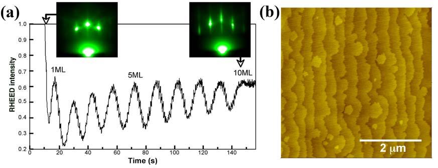
3 the lattice mismatch was shown to lead to a significant increase of the spontaneous polarization and phase transition temperature in BaTiO 3 films [15]. Stabilization of the polar phase by reducing the depolarizing field energy has been achieved via formation of nanometer-period antiparallel 180º stripe domains [16] or by effective control of chemical environment that allows efficient screening of the polarization charges [17]. These results open a way for experimental implementation of the FTJ structures. Structurally and electrically perfect epitaxial ferroelectric heterostructures with a thickness of just several unit cells are a prerequisite for implementation of FTJs. To achieve the atomically abrupt and well-defined interfaces, epitaxial BaTiO 3 films have been fabricated by atomic layer controlled growth with in-situ monitoring using high pressure reflection high energy electron diffraction (RHEED) [ 15, 18]. To probe the nanoscale switching behavior and transport we used epitaxial ferroelectric films of BaTiO 3 with a thickness in the range from 2.4 nm to 9.6 nm grown on atomically smooth TiO 2 -terminated (001) SrTiO 3 substrates with single crystalline SrRuO 3 electrodes. Figure 1a shows RHEED intensity oscillation and RHEED patterns indicating a layer-by-layer growth and epitaxial structure of the BaTiO 3 films. The AFM image of completed BaTiO 3 /SrRuO 3 heterostructure in Fig. 1b clearly indicates atomically-flat terraces with single unit-cell high (~4 Å) steps. Cross-sectional TEM images (not shown) demonstrate that the BaTiO 3 and SrRuO 3 layers are fully commensurate with the SrTiO 3 substrates. We investigate the polarization-dependent TER effect by monitoring and controlling the electric polarization and correlating local ferroelectric switching with the local conductivity. Our approach is to employ a combination of scanning probe microscopy techniques for nanoscale polarization detection (Piezoresponse Force Microscopy, or PFM) [ 19, 20] and spatiallyresolved local conductance measurements (Conducting Atomic Force Microscopy, or C-AFM) 3
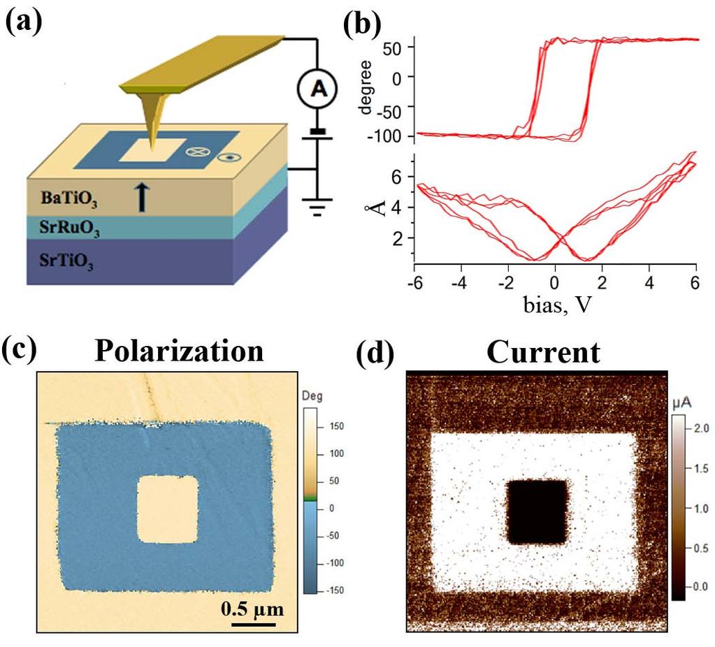
4 [21, 22]. The experimental geometry shown in Fig. 2a involves a conductive probing tip in contact with a bare BaTiO 3 surface (in the area of about 20 nm in diameter) connected to a power supply for local piezoresponse and current measurements. The measurements have been performed using a commercial atomic force microscope AFM (Asylum MFP-3D). Resonant-enhanced PFM mode was used to obtain images of polarization patterns in BaTiO 3 films. Typical frequency range for an ac voltage was khz with an amplitude of 0.5 V (peak-to-peak). Conductive Pt-Ti-coated silicon cantilevers (NSC14, Mikromasch) were used for PFM imaging and polarization switching studies. Local piezoelectric hysteresis loops were measured in fixed locations on the film surface as a function of a dc switching bias superimposed on ac modulation bias. Nanoscale electrical transport measurements have been performed in the C-AFM mode using a voltage source measure unit (Keithley 237) allowing reliable current detection in the range from to 10-3 A. Local current-voltage characteristics were measured by positioning a conductive diamond tip (CDT-NCHR, Nanoworld AG) at a selected point on the film surface and by sweeping a dc voltage. Current maps were obtained simultaneously with the topographic data by scanning the surface with the tip held under a constant dc bias (not higher than 30% of the coercive voltage) and measuring current at each pixel point of the scanned area. Typical imaging scan rate was 0.8 Hz. Figure 2b shows a local PFM response of a 4.8nm-thick BaTiO 3 film that reveals a hysteretic behavior typical for polarization switching. Note that the hysteresis loop is characterized by a shift toward a positive voltage indicating a built-in electric field of about 10 6 V/cm. The direction of the field is upward (i.e. from the substrate to the tip) which is consistent 4
5 with a single-domain state of as-grown BaTiO 3 films exhibiting the upward polarization orientation. To demonstrate the TER effect, first, we change the upward-polarized single-domain state of the as-grown BaTiO 3 film to a bidomain-patterned state. For this purpose, polarization in a 2.5x2.5 µm 2 square region of the film is switched downward by scanning the film surface with a tip biased with a voltage V tip = +3.0V that exceeds the coercive voltage for the film. Then, polarization within an area of 0.5x0.5 µm 2 square area in the center is switched back upward by applying a bias V tip = 3.0V to the tip. Figure 2c shows the resulting polarization pattern as measured by PFM. Antiparallel domains written this way demonstrate almost no relaxation 3 days after the switching, which suggests a highly stable and robust polarization. The resistive switching behavior of the BaTiO 3 films is examined using a C-AFM technique. A current map is acquired by scanning the polarization-patterned area with a dc bias of 0.3 V. Figure 2d shows the resulting current pattern within the poled area where variations in contrast correspond to different conductivity. The striking feature evident from the comparison of Figs. 2c and 2d is a perfect correspondence of the spatial variations in local conductivity measured by C-AFM to the polarization domain pattern measured by PFM. The area with downward polarization shows significantly higher conductivity than the area with upward polarization with the resistance ratio between the two polarization states of about 7 and 83 for the 2.4 nm and 4.8 nm thick BaTiO 3 films, respectively. By performing several sequential PFM/current imaging series we find that a small dc bias used for conductance measurements does not perturb the ferroelectric state thus allowing multiple nondestructive polarization readouts. To distinguish the ferroelectric-induced mechanism of resistive switching from other 5
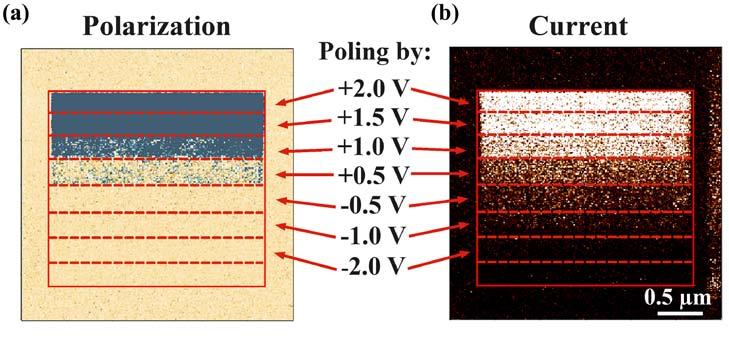
6 mechanisms [2], we have examined correlation between the onset of polarization reversal and a change in electrical conductance in the same locations. The BaTiO 3 surface was scanned with the tip under an incrementally increasing dc bias with simultaneous PFM detection of polarization. The gradual change in the contrast under a tip bias close to the coercive voltage seen in Fig. 3a is an indication of polarization reversal. Subsequently, the current map was acquired in the same area by C-AFM. As seen from Fig. 3b, the transition from high to low resistance states occurred exactly at the same bias where polarization undergoes reversal from the upward to downward direction. Resistance stays constant in the fully switched regions irrespective of what voltage is used for poling. This result is an unambiguous demonstration of the ferroelectric nature of the resistive switching. Spatially-resolved imaging of polarization and tunneling current are complemented by local spectroscopic measurements which provide a quantitative insight into resistive switching [23]. I-V characteristics recorded for oppositely poled regions (Fig. 4) show a non-linear behavior typical for tunneling conductance in tunnel junctions and a drastic change in resistance. In the case of the 4.8-nm thick BaTiO 3 film the resistance changes by almost two orders of magnitude upon polarization reversal. These remarkable results clearly illustrate the giant TER effect in FTJs predicted earlier [ 8]. It has been demonstrated theoretically [8, 10] that a change in electric polarization direction, and hence a change in the relative Ti displacements in the BaTiO 3 cell, can affect the density of states at the electrode-barrier interfaces, as well as the interface dipoles and complex band structure of the barrier, primarily due to changing interfacial atomic positions and electronic structure. In the case that the interfaces differ, the changes on polarization reversal are also likely to differ, leading to a dependence of tunneling current on polarization direction. To 6
7 interpret out results, we assume direct tunneling through the barrier, with interfacial effects and their change with polarization reversal by potential steps at the interfaces that depend on the polarization direction. To model the observed TER effect we employ a simple model, involving a tunneling current through a trapezoidal potential barrier [24] whose profile depends on polarization orientation. The barrier has width d and potential steps at the interfaces of φ 1 and 2 φ, so that the potential energy across the barrier in the presence of bias voltage V varies as φ( x, V ) = φ + ev /2 + x( φ ev φ )/ d. Using the WKB approximation and assuming that the applied voltage is not too large, so that ev /2< φ1,2 and the barrier width is not too small, so that d 2m 2 φ 1,2 >>1, we obtain an analytic expression for the current density: 3/2 3/2 ev ev exp α( V ) φ2 φ1+ 1/2 1/ ev ev ev J C sinh α( V) φ 2 2 φ1+ (1) 1/2 1/ ev ev α ( V ) φ2 φ em where C = 2 3 9π α( V ) 4d 2m and 3 ( φ + ev φ ) 1 2. Figure 4 shows a fit of the experimental I-V characteristics for the 4.8nm thick BaTiO 3 film, using Eq. (1) and the following parameters: φ 1 = 0.24eV and φ 2 = 1.52eV for polarization pointing up, φ 1 = 0.48eV and φ 2 = 0.96eV for polarization pointing down, d = 4.8 nm and m = m 0. The respective change in the potential energy profile is shown schematically in the inset of Fig. 4. According to these results, the reversal of polarization changes the potential energy difference φ 1 φ 2 across the BaTiO 3 barrier from 1.28 ev to 0.48 ev. This change of 0.8 ev is 7
8 due to the change in the electrostatic potential associated with ferroelectric polarization reversal and associated reorientation of the depolarizing field. We note that φ 2 φ 1 is higher for polarization pointing up than for polarization pointing down indicating that holes dominate in the tunneling conductance. This behavior is expected if the decay constant of the evanescent state in the tunneling barrier is increasing with energy, which is the case for the Δ 1 band in BaTiO 3 [25]. The fitting predicts a potential drop of 1.28V acting in the initial polarization state of the as-grown sample. We interpret this result as a consequence of the screening charge accumulation on the film surface, which is shown to have a profound effect in stabilizing the polarization in ultrathin films [ 17]. The screening charge most likely is a bound charge accumulated within a thin (a few Angstroms) surface dielectric layer formed after the ferroelectric film has been exposed to air. This dielectric layer is expected to have a higher band gap and consequently it produces a higher potential barrier than BaTiO 3 which within our trapezoidal barrier model leads to the potential slope in the as-grown state. Assuming that the bound screening charges create an internal electric field that almost fully compensates the depolarizing field in the barrier in the asgrown state, we conclude from our fitting that the intrinsic electric field produces an electrostatic potential drop of 0.8V/2=0.4V across the BaTiO 3 layer. The presence of this field is consistent with our experimental results which indicate a shift in the hysteresis curve by about the same value in Fig. 2b. In the Ohmic transport regime typical for a small bias voltage, Eq. (1) is reduced to J e 1 2 m 4 2 ( 2 1 ) exp m φ φ φ + φ 2h 2πd 3 φ2 φ1 2 3/2 3/2 1/2 1/2 2 1 d V. (2) 8
9 If the difference between potential steps φ φ2 φ1 is not too large compared to the average potential φ ( φ φ ) +, so that φ /2< φ, this formula can be approximated by 2 1 /2 J 2 e h 1 2π d 2mφ 2mφ exp 2 d V, (3) which is consistent with Simmons s formula at low bias voltage [26]. According to Eq. (3), the transport properties are entirely determined by the average potential barrier height and we can discuss the TER effect in terms of the change of φ with polarization reversal. We assume that the barrier height changes by δφ from φ δφ /2 (high conductance state, current density J > ) to φ + δφ /2 (low conductance state, current density J < ) and define the TER ratio by ( ) / TER J J J. Assuming that δφ is small and J > >> J < we arrive at > < < J> J 2m δφ < TER exp d. (4) J< φ In case of the 4.8 nm thick BaTiO 3 film, we find that φ = 0.80eV and δφ = 0.16 ev resulting in TER 80 consistent with our fit and experiment. It is noteworthy that Eq. (4) predicts a dramatic increase in TER with increasing barrier thickness d. This increase is expected to be stronger than exponential due to the dependence of φ and δφ on d (through the polarization-induced potential variation across the barrier), resulting in the increasing δφ / φ with film thickness. This tendency is indeed observed experimentally. If we assume that both φ and δφ are constants, according to Eq. (4), an increase in film thickness by a factor of two is expected to produce a TER that is a square of the value at the 9
10 smaller thickness. In our case, an increase from d = 2.4 nm to d = 4.8 nm enhances TER from 7 to 83, i.e. by a factor of two larger than what is expected from a simple exponential dependence. In summary, we have demonstrated polarization-dependent resistive switching behavior of ultrathin films of BaTiO 3 at room temperature, manifesting the tunneling electroresistance effect predicted earlier. Upon polarization reversal, tunneling resistance changes by almost two orders of magnitude on a lateral scale of about 20 nm. Polarization retention is not affected by conductance measurements thus allowing multiple nondestructive polarization readouts and opening a possibility for application as non-charge based logical switches in nonvolatile memory devices. This work was supported by the National Science Foundation (Grant No. MRSEC DMR ), the Nanoelectronics Research Initiative of Semiconductor Research Corporation, ECCS and the Office of Naval Research through grants N
11 Fig. 1 11
12 Fig. 2 12
13 Fig. 3 13
14 Fig. 4 14
15 Figure Captions Figure 1. (a) RHEED intensity oscillation during the growth of BaTiO 3 ferroelectric layer on SrRuO 3 bottom electrode and RHEED patterns before and after deposition of the BaTiO 3 layer; (b) AFM image of the BaTiO 3 film on the SrRuO 3 /SrTiO 3 substrate. Figure 2. (a) Sketch illustrating the geometry of experiment for PFM/C-AFM studies of tunneling electroresistance effect in ultra-thin BaTiO 3 films. (b) Local PFM hysteresis loops measured in the 4.8-nm thick BaTiO 3 film (top - phase signal, bottom - amplitude signal). (c) PFM image of a polarization pattern produced by scanning with the tip under 3.0 V (blue region corresponds to polarization switched downward; yellow region represents upward polarization in the as-grown film). (d) Tunneling current map acquired in the same region as in (c). Bright contrast indicating higher current is observed in the regions with polarization oriented downward. Figure 3. Spatially resolved correlation between the onset of polarization reversal (a) and a change in electrical conductance (b). A change in the polarization contrast in the red block from yellow to blue illustrates polarization reversal under an incrementally changing tip bias. Dashed red lines indicate where the bias is changing. The change in PFM contrast correlates with the transition from low current (dark contrast) to high current (bright contrast). Figure 4. I-V curves for two opposite polarization directions in the 4.8-nm thick BaTiO 3 film measured by C-AFM. Solid lines - fitting of the experimental data by the WKB model. The inset shows schematically the potential energy profiles for two polarization orientations. 15
16 References 1 E. Y. Tsymbal and H. Kohlstedt, Tunneling Across a Ferroelectric, Science 313, (2006). 2 R. Waser and M. Aono, Nanoionics-Based Resistive Switching Memories, Nat. Mater. 6, (2007). 3 C. Rossel, G.I. Meijer, D. Bremaud, and D. Widmer, Electrical current distribution across a metal-insulator-metal structure during bistable switching, J. Appl. Phys. 90, (2001). 4 A. Sawa, T. Fujii, M. Kawasaki, and Y. Tokura, Hysteretic current-voltage characteristics and resistance switching at a rectifying Ti/Pr 0.7 Ca 0.3 MnO 3 interface, Appl. Phys. 85, (2004). 5 F. A. Chudnovskii, L. L. Odynets, A. L. Pergament, G. B. Stefanovich, Electroforming and switching in oxides of transition metals: the role of metal-insulator transition in the switching mechanism, J. Solid State Chem. 122, (1996). 6 K. Szot, R. Dittmann, W. Speier, and R. Waser, Nanoscale resistive switching in SrTiO 3 thin films, Phys. Stat. Sol. 1, No. 2, R86 R88 (2007). 7 K. Szot, W. Speier, G. Bihlmayer, and R. Waser, Switching the electrical resistance of individual dislocations in single-crystalline SrTiO 3, Nat. Mat. 5, (2006). 8 M. Y. Zhuravlev, R. F. Sabirianov, S. S. Jaswal, and E. Y. Tsymbal, Giant electroresistance in ferroelectric tunnel junctions, Phys. Rev. Lett. 94, (2005). 9 H. Kohlstedt, N. A. Pertsev, J. Rodríguez Contreras, and R. Waser, Theoretical currentvoltage characteristics of ferroelectric tunnel junctions, Phys. Rev. B 72, (2005). 16
17 10 J. P. Velev, C.-G. Duan, K. D. Belashchenko, S. S. Jaswal, and E. Y. Tsymbal, Effect of ferroelectricity on electron transport in Pt/BaTiO 3 /Pt tunnel junctions, Phys. Rev. Lett. 98, (2007). 11 J. Rodriguez-Contreras, H. Kohlstedt, U. Poppe, R. Waser, C. Buchal, and N. A. Pertsev, Resistive switching in metal ferroelectric metal junctions, Appl. Phys. Lett. 83, 4595 (2003). 12 M. Gajek, M. Bibes, S. Fusil, K. Bouzehouane, J. Fontcuberta, A. Barthélémy, and A. Fert, Multiferroic tunnel junctions, Nat. Mater. 6, (2007). 13 C. Lichtensteiger, J.-M. Triscone, J. Junquera, and P. Ghosez, "Ferroelectricity and tetragonality in ultra-thin PbTiO3 films", Phys. Rev. Lett. 94, (2005). 14 C. L. Jia, V. Nagarajan, J. Q. He, L. Houben, T. Zhao, R. Ramesh, K. Urban, and R. Waser, "Unit-cell scale mapping of ferroelectricity and tetragonality in epitaxial ultra-thin ferroelectric films", Nat. Mater. 6, (2007). 15 K. J. Choi, M. Biegalski, Y. L. Li, A. Sharan, J. Schubert, R. Uecker, P. Reiche, Y. B. Chen, X. Q. Pan, V. Gopalan, L.-Q. Chen, D. G. Schlom, and C. B. Eom, Enhancement of ferroelectricity in strained BaTiO 3 thin films, Science 306, (2004). 16 C. Thompson, D. D. Fong, R. V. Wang, F. Jiang, S. K. Streiffer, K. Latifi, J. A. Eastman, P. H. Fuoss, and G. B. Stephenson, Imaging and alignment of nanoscale 180 stripe domains in ferroelectric thin films, Appl. Phys. Lett. 93, (2008). 17 D. D. Fong, A. M. Kolpak, J. A. Eastman, S. K. Streiffer, P. H. Fuoss, G. B. Stephenson, C. Thompson, D. M. Kim, K. J. Choi, C. B. Eom, I. Grinberg, and A. M. Rappe, Stabilization of Monodomain Polarization in Ultra-thin PbTiO 3 Films, Phys. Rev. Lett. 96, (2006). 17
18 18 C. B. Eom, R. J. Cava, R. M. Fleming, Julia M. Phillips, R. B. van Dover, J. H. Marshall, J. W. P. Hsu, J. J. Krajewski, and W. F. Peck Jr. Single-Crystal Epitaxial Thin Films of the Isotropic Metallic Oxides Sr 1-x Ca x RuO 3 Science 258, 1766 (1992). 19 A. Gruverman and A. Kholkin, Nanoscale Ferroelectrics: Processing, Characterization and Future Trends, Rep. Prog. Phys. 69, 2443 (2006), 20 B. J. Rodriguez, S. Jesse, M. Alexe, and S. V. Kalinin, Spatially Resolved Mapping of Polarization Switching Behavior in Nanoscale Ferroelectrics, Adv. Mat. 20, (2008). 21 K. Szot, W. Speier, G. Bihlmayer, And R. Waser, Switching the electrical resistance of individual dislocations in single-crystalline SrTiO 3, Nat. Mat. 5, (2006). 22 J. Seidel, L. W. Martin, Q. He, Q. Zhan, Y.-H. Chu, A. Rother, M. E. Hawkridge, P. Maksymovych, P. Yu, M. Gajek, N. Balke, S. V. Kalinin, S. Gemming, F. Wang, G. Catalan, J. F. Scott, N. A. Spaldin, J. Orenstein, and R. Ramesh, Conduction at domain walls in oxide multiferroics, Nat. Mater. 8, (2009). 23 H. Kohlstedt, A. Petraru, K. Szot, A. Ruediger, P. Meuffels, H. Haselier, R. Waser, and V. Nagarajan, Method to distinguish ferroelectric from nonferroelectric origin in case of resistive switching in ferroelectric capacitors, Appl. Phys. Lett 92, (2008). 24 W. F. Brinkman, R. C. Dynes, and J. M. Rowell, Tunneling Conductance of Asymmetric Barriers, J. Appl. Phys. 41, (1970). 25 J. P. Velev, C.-G. Duan, J. D. Burton, A. Smogunov, M.K. Niranjan, E. Tosatti, S. S. Jaswal, and E. Y. Tsymbal, Magnetic tunnel junctions with ferroelectric barriers: Prediction of four resistance states from first-principles, Nano Letters 9, (2009). 26 J. G. Simmons, Generalized Formula for the Electric Tunnel Effect between Similar Electrodes Separated by a Thin Insulating Film, J. Appl. Phys. 34, (1963). 18
Electrically induced resistive switching has been observed in. Ferroelectric Tunnel Memristor
 pubs.acs.org/nanolett Ferroelectric Tunnel Memristor D. J. Kim, H. Lu, S. Ryu, C.-W. Bark, C.-B. Eom, E. Y. Tsymbal, and A. Gruverman*, Department of Physics and Astronomy & Nebraska Center for Materials
Colossal electroresistance in metal/ferroelectric/semiconductor. tunnel diodes for resistive switching memories
 Colossal electroresistance in metal/ferroelectric/semiconductor tunnel diodes for resistive switching memories Zheng Wen, Chen Li, Di Wu*, Aidong Li and Naiben Ming National Laboratory of Solid State Microstructures
Polarization Control of Electron Tunneling into Ferroelectric Surfaces
 Submitted: Science Date: 01/20/2009 Revised: 05/07/2009 Polarization Control of Electron Tunneling into Ferroelectric Surfaces Peter Maksymovych* 1, Stephen Jesse 1, Pu Yu 2, Ramamoorthy Ramesh 2, Arthur
Enhancement of Ferroelectric Polarization Stability by Interface Engineering
 www.materialsviews.com Enhancement of Ferroelectric Polarization Stability by Interface Engineering H. Lu, X. Liu, J. D. Burton, C.-W. Bark, Y. Wang, Y. Zhang, D. J. Kim, A. Stamm, P. Lukashev, D. A. Felker,
SUPPLEMENTARY INFORMATION
 Ferroelectric-field-effect-enhanced electroresistance in metal/ferroelectric/semiconductor tunnel junctions Zheng Wen, Chen Li, Di Wu*, Aidong Li and Naiben Ming National Laboratory of Solid State Microstructures,
Supplementary Figures
 Supplementary Figures Supplementary Figure 1 Thickness calibration of PVDF layers using atomic force microscopy. (a-d) Tapping AFM images of 1 L, 2 Ls, 4 Ls and 20 Ls PVDF films, respectively on Au-coated
Polarity control of carrier injection at ferroelectric/metal interfaces. for electrically switchable diode and photovoltaic effects
 Polarity control of carrier injection at ferroelectric/metal interfaces for electrically switchable diode and photovoltaic effects D. Lee, 1 S. H. Baek, 2 T. H. Kim, 1 J.-G. Yoon, 3 C. M. Folkman, 2 C.
2 Title: "Ultrathin flexible electronic device based on tunneling effect: a flexible ferroelectric tunnel
 Electronic Supplementary Material (ESI) for Journal of Materials Chemistry C. This journal is The Royal Society of Chemistry 208 Supplementary information 2 Title: "Ultrathin flexible electronic device
From 180º stripe domains to more exotic patterns of polarization in ferroelectric nanostructures. A first principles view
 From 180º stripe domains to more exotic patterns of polarization in ferroelectric nanostructures. A first principles view Pablo Aguado-Puente Javier Junquera Ferroelectricity: Basic definitions Existence
Combining Ferroelectricity, Magnetism, and
 Forschungszentrum Jülich Combining Ferroelectricity, Magnetism, and Superconductivity ty in Tunnel Junctions H. Kohlstedt 1, N. A. Pertsev 2,A. Petraru 1, U. Poppe 1, and R. Waser 1 1 CNI Center of Nanoelectronic
SUPPLEMENTARY INFORMATION
 SUPPLEMENTARY INFORMATION Reversible Electric Control of Exchange Bias in a Multiferroic Field Effect Device S. M. Wu 1, 2, Shane A. Cybart 1, 2, P. Yu 1, 2, M. D. Abrodos 1, J. Zhang 1, R. Ramesh 1, 2
Nanosecond Structural Visualization of the Reproducibility of Polarization Switching in Ferroelectrics
 Integrated Ferroelectrics, 85: 165 173, 2006 Copyright Taylor & Francis Group, LLC ISSN 1058-4587 print / 1607-8489 online DOI: 10.1080/10584580601085842 Nanosecond Structural Visualization of the Reproducibility
Newcastle University eprints
 Newcastle University eprints Ponon NK, Appleby DJR, Arac E, Kwa KSK, Goss JP, Hannemann U, Petrov PK, Alford NM, O'Neill A. Impact of Crystalline Orientation on the Switching Field in Barium Titanate Using
Supplementary Figures:
 Supplementary Figures: Supplementary Figure 1 Cross-sectional morphology and Chemical composition. (a) A low-magnification dark-field TEM image shows the cross-sectional morphology of the BWO thin film
Hermann Kohlstedt. Technical Faculty Nanoelectronics
 Forschungszentrum Jülich Institut für Festkörperforschung Jülich, Germany Complex Oxide Tunnel Junctions Hermann Kohlstedt Christian-Albrechts-University Kiel Technical Faculty Nanoelectronics Germany
Ferroelectricity in Strain-Free SrTiO 3 Thin Films
 Ferroelectricity in Strain-Free SrTiO 3 Thin Films H. W. Jang, 1 A. Kumar, 2 S. Denev, 2 M. D. Biegalski, 3 P. Maksymovych, 3 C.W. Bark, 1 C. T. Nelson, 4 C. M. Folkman, 1 S. H. Baek, 1 N. Balke, 3 C.
Magnetic tunnel junctions based on ferroelectric Hf 0.5Zr 0.5O 2 tunnel barriers
 Magnetic tunnel junctions based on ferroelectric Hf 0.5Zr 0.5O 2 tunnel barriers Yingfen Wei 1, Sylvia Matzen 2, *, Guillaume Agnus 2, Mart Salverda 1, Pavan Nukala 1, Thomas Maroutian 2, Qihong Chen 1,
SUPPLEMENTARY MATERIAL
 SUPPLEMENTARY MATERIAL Multiphase Nanodomains in a Strained BaTiO3 Film on a GdScO3 Substrate Shunsuke Kobayashi 1*, Kazutoshi Inoue 2, Takeharu Kato 1, Yuichi Ikuhara 1,2,3 and Takahisa Yamamoto 1, 4
Mechanism of Polarization Fatigue in BiFeO 3 : the Role of Schottky Barrier
 Mechanism of Polarization Fatigue in BiFeO 3 : the Role of Schottky Barrier Yang Zhou, 1 Xi Zou, 1 Lu You, 1 Rui Guo, 1 Zhi Shiuh Lim, 1 Lang Chen, 1 Guoliang Yuan, 2,a) and Junling Wang 1,b) 1 School
Micron 43 (2012) Contents lists available at SciVerse ScienceDirect. Micron. j our na l ho me p age:
 Contents lists available at SciVerse ScienceDirect. Micron. j our na l ho me p age:") Micron 43 (2012) 1121 1126 Contents lists available at SciVerse ScienceDirect Micron j our na l ho me p age: www.elsevier.com/locate/micron Direct observation of ferroelectric domain switching in varying
Micron 43 (2012) 1121 1126 Contents lists available at SciVerse ScienceDirect Micron j our na l ho me p age: www.elsevier.com/locate/micron Direct observation of ferroelectric domain switching in varying
David Jiménez, Enrique Miranda, Atsushi Tsurumaki-Fukuchi, Hiroyuki Yamada, Jordi Suñé, and Akihito Sawa
 Multilevel recording in Bi-deficient Pt/BFO/SRO heterostructures based on ferroelectric resistive switching targeting high-density information storage in nonvolatile memories David Jiménez, Enrique Miranda,
Ferroelectric Tunnel Junctions: A Theoretical Approach
 Forschungszentrum Jülich Ferroelectric Tunnel Junctions: A Theoretical Approach H. Kohlstedt, A. Petraru, R. Waser Forschungszentrum Jülich GmbH, Institut für Festkörperforschung and CNI, the Center of
Towards ferroelectrically-controlled magnetism: Magnetoelectric effect in Fe/BaTiO 3 multilayers
 Towards ferroelectrically-controlled magnetism: Magnetoelectric effect in Fe/BaTiO 3 multilayers Chun-Gang Duan, Sitaram S. Jaswal, and Evgeny Y. Tsymbal Department of Physics and Astronomy, Center for
Electrostatic charging and redox effects in oxide heterostructures
 Electrostatic charging and redox effects in oxide heterostructures Peter Littlewood 1,2,3 Nick Bristowe 3 & Emilio Artacho 3,6 Miguel Pruneda 4 and Massimiliano Stengel 5 1 Argonne National Laboratory
Continuous Control of Charge Transport in Bi-Deficient BiFeO 3 Films Through Local Ferroelectric Switching
 Continuous Control of Charge Transport in Bi-Deficient BiFeO 3 Films Through Local Ferroelectric Switching Tae Heon Kim, Byung Chul Jeon, Taeyoon Min, Sang Mo Yang, Daesu Lee, Yong Su Kim, Seung-Hyub Baek,
Towards reversible control of domain wall conduction in Pb(Zr0.2Ti0.8)O3 thin films
O3 thin films") Towards reversible control of domain wall conduction in Pb(Zr0.2Ti0.8)O3 thin films I. Gaponenko, P. Tückmantel, J. Karthik, L. W. Martin, and P. Paruch Citation: Applied Physics Letters 106, 162902 (2015);
Towards reversible control of domain wall conduction in Pb(Zr0.2Ti0.8)O3 thin films I. Gaponenko, P. Tückmantel, J. Karthik, L. W. Martin, and P. Paruch Citation: Applied Physics Letters 106, 162902 (2015);
Transformation dependence of lead zirconate titanate (PZT) as shown by PiezoAFM surface mapping of Sol-gel produced PZT on various substrates.
 as shown by PiezoAFM surface mapping of Sol-gel produced PZT on various substrates.") Transformation dependence of lead zirconate titanate (PZT) as shown by PiezoAFM surface mapping of Sol-gel produced PZT on various substrates. Abstract S. Dunn and R. W. Whatmore Building 70, Nanotechnology,
Transformation dependence of lead zirconate titanate (PZT) as shown by PiezoAFM surface mapping of Sol-gel produced PZT on various substrates. Abstract S. Dunn and R. W. Whatmore Building 70, Nanotechnology,
Research proposal #### Title of the project Ferroelectric tunnel junction. Applicant information: FOM research group. Institute:
 Research proposal Title of the project Ferroelectric tunnel junction Applicant information: Name: Reza Last name: Saberi Moghaddam Date of birth: 13-07-1981 Natinality: Iranian FOM research group ####
Domain Nucleation And Relaxation Kinetics In Ferroelectric Thin Films. Ramesh
 Domain Nucleation And Relaxation Kinetics In Ferroelectric Thin Films C. S. Ganpule a), V. Nagarajan, S. B. Ogale, A. L. Roytburd, E. D. Williams and R. Ramesh Materials Research Science and Engineering
Structural dynamics of PZT thin films at the nanoscale
 Mater. Res. Soc. Symp. Proc. Vol. 902E 2006 Materials Research Society 0902-T06-09.1 Structural dynamics of PZT thin films at the nanoscale Alexei Grigoriev 1, Dal-Hyun Do 1, Dong Min Kim 1, Chang-Beom
Ferroelectric domain scaling and switching in ultrathin BiFeO 3. films deposited on vicinal. substrates
 Home Search Collections Journals About Contact us My IOPscience Ferroelectric domain scaling and switching in ultrathin BiFeO 3 films deposited on vicinal substrates This content has been downloaded from
Magnetic tunnel junctions with ferroelectric barriers: Prediction of four resistance states from first-principles
 Magnetic tunnel junctions with ferroelectric barriers: Prediction of four resistance states from first-principles Julian P. Velev,, * Chun-Gang Duan, 3 J. D. Burton, Alexander Smogunov, 4,5 Manish K. Niranjan,
SUPPLEMENTARY INFORMATION
 SUPPLEMENTARY INFORMATION Insulating Interlocked Ferroelectric and Structural Antiphase Domain Walls in Multiferroic YMnO 3 T. Choi 1, Y. Horibe 1, H. T. Yi 1,2, Y. J. Choi 1, Weida. Wu 1, and S.-W. Cheong
Ferroelectric (FE) thin films and nanostructures continue
 thin films and nanostructures continue") Finite Curvature-Mediated Ferroelectricity Stephen S. Nonnenmann, Oren D. Leaffer, Eric M. Gallo, Michael T. Coster, and Jonathan E. Spanier* pubs.acs.org/nanolett Department of Materials Science and Engineering,
Finite Curvature-Mediated Ferroelectricity Stephen S. Nonnenmann, Oren D. Leaffer, Eric M. Gallo, Michael T. Coster, and Jonathan E. Spanier* pubs.acs.org/nanolett Department of Materials Science and Engineering,
Effect of substrate-induced strains on the spontaneous polarization of epitaxial BiFeO 3 thin films
 JOURNAL OF APPLIED PHYSICS 11, 11415 27 Effect of substrate-induced strains on the spontaneous polarization of epitaxial 3 thin films J. X. Zhang, a Y. L. Li, Y. Wang, Z. K. Liu, and L. Q. Chen Department
Recent Progress in Ferroelectric Diodes: Explorations in Switchable Diode Effect
 www.nmletters.org Recent Progress in Ferroelectric Diodes: Explorations in Switchable Diode Effect Chen Ge, Can Wang, Kui-juan Jin, Hui-bin Lu, Guo-zhen Yang (Received 11 March 2013; accepted 17 April
A Nanoscale Shape Memory Oxide
 A Nanoscale Shape Memory Oxide Jinxing Zhang 1,2*, Xiaoxing Ke 3*, Gaoyang Gou 4, Jan Seidel 2,5, Bin Xiang 6,9, Pu Yu 2,7, Wen-I Liang 8, Andrew M. Minor 9,10, Ying-hao Chu 8, Gustaaf Van Tendeloo 3,
Supplementary Material for
 www.sciencemag.org/content/349/6254/1314/suppl/dc1 Supplementary Material for Emergence of room-temperature ferroelectricity at reduced dimensions D. Lee, H. Lu, Y. Gu, S.-Y. Choi, S.-D. Li, S. Ryu, T.
Supplementary Information for. Effect of Ag nanoparticle concentration on the electrical and
 Supplementary Information for Effect of Ag nanoparticle concentration on the electrical and ferroelectric properties of Ag/P(VDF-TrFE) composite films Haemin Paik 1,2, Yoon-Young Choi 3, Seungbum Hong
Active Control of Ferroelectric Switching Using Defect-Dipole Engineering
 Active Control of Ferroelectric Switching Using Defect-Dipole Engineering www.materialsviews.com Daesu Lee, Byung Chul Jeon, Seung Hyub Baek, Sang Mo Yang, Yeong Jae Shin, Tae Heon Kim, Yong Su Kim, Jong-Gul
Since the discovery of a conducting two-dimensional. Switchable Induced Polarization in LaAlO 3 /SrTiO 3 Heterostructures
 pubs.acs.org/nanolett Switchable Induced Polarization in LaAlO 3 /SrTiO 3 Heterostructures C. W. Bark, P. Sharma, Y. Wang, S. H. Baek, S. Lee, S. Ryu, C. M. Folkman, T. R. Paudel, A. Kumar, S. V. Kalinin,
Giant Resistive Switching via Control of Ferroelectric Charged Domain Walls
 Giant Resistive Switching via Control of Ferroelectric Charged Domain Walls Linze Li, Jason Britson, Jacob R. Jokisaari, Yi Zhang, Carolina Adamo, Alexander Melville, Darrell G. Schlom, Long-Qing Chen,
(a) (b) Supplementary Figure 1. (a) (b) (a) Supplementary Figure 2. (a) (b) (c) (d) (e)
 (b) Supplementary Figure 1. (a) (b) (a) Supplementary Figure 2. (a) (b) (c) (d) (e)") (a) (b) Supplementary Figure 1. (a) An AFM image of the device after the formation of the contact electrodes and the top gate dielectric Al 2 O 3. (b) A line scan performed along the white dashed line
(a) (b) Supplementary Figure 1. (a) An AFM image of the device after the formation of the contact electrodes and the top gate dielectric Al 2 O 3. (b) A line scan performed along the white dashed line
Bipolar resistive switching in amorphous titanium oxide thin films
 Bipolar resistive switching in amorphous titanium oxide thin films Hu Young Jeong and Jeong Yong Lee Department of Materials Science and Engineering, KAIST, Daejeon 305-701, Korea Min-Ki Ryu and Sung-Yool
CMOS compatible integrated ferroelectric tunnel junctions (FTJ)
") CMOS compatible integrated ferroelectric tunnel junctions (FTJ) Mohammad Abuwasib 1*, Hyungwoo Lee 2, Chang-Beom Eom 2, Alexei Gruverman 3, Jonathan Bird 1 and Uttam Singisetti 1 1 Electrical Engineering,
CMOS compatible integrated ferroelectric tunnel junctions (FTJ) Mohammad Abuwasib 1*, Hyungwoo Lee 2, Chang-Beom Eom 2, Alexei Gruverman 3, Jonathan Bird 1 and Uttam Singisetti 1 1 Electrical Engineering,
Domain Engineering for Enhanced Ferroelectric Properties of Epitaxial (001) BiFeO Thin Films
 BiFeO Thin Films") Domain Engineering for Enhanced Ferroelectric Properties of Epitaxial (001) BiFeO Thin Films By Ho Won Jang, Daniel Ortiz, Seung-Hyub Baek, Chad M. Folkman, Rasmi R. Das, Padraic Shafer, Yanbin Chen, Christofer
Domain Engineering for Enhanced Ferroelectric Properties of Epitaxial (001) BiFeO Thin Films By Ho Won Jang, Daniel Ortiz, Seung-Hyub Baek, Chad M. Folkman, Rasmi R. Das, Padraic Shafer, Yanbin Chen, Christofer
Interfacial Coherency and Ferroelectricity of BaTiO 3 /SrTiO 3 Superlattice Films
 Boise State University ScholarWorks Physics Faculty Publications and Presentations Department of Physics 12-18-2007 Interfacial Coherency and Ferroelectricity of BaTiO 3 /SrTiO 3 Superlattice Films Y.
"Oxygen-vacancy effect on structural, magnetic, and ferroelectric properties in multiferroic YMnO3 single crystals"
 University of Wollongong Research Online Faculty of Engineering - Papers (Archive) Faculty of Engineering and Information Sciences 2012 "Oxygen-vacancy effect on structural, magnetic, and ferroelectric
SUPPLEMENTARY NOTES Supplementary Note 1: Fabrication of Scanning Thermal Microscopy Probes
 SUPPLEMENTARY NOTES Supplementary Note 1: Fabrication of Scanning Thermal Microscopy Probes Fabrication of the scanning thermal microscopy (SThM) probes is summarized in Supplementary Fig. 1 and proceeds
High-quality all-oxide Schottky junctions fabricated on heavily Nb-doped SrTiO 3 substrates
 High-quality all-oxide Schottky junctions fabricated on heavily Nb-doped SrTiO 3 substrates A. Ruotolo *, C.Y. Lam, W.F. Cheng, K.H. Wong and C.W. Leung Department of Applied Physics and Materials Research
Metal-Insulator-Metal Junctions
 Forschungszentrum Jülich Resistive Switching in Metal-Insulator-Metal Junctions H. Kohlstedt* Forschungszentrum Jülich GmbH, Institut für Festkörperforschung and CNI, the Center of Nanoelectronic Systems
Fabrication and Characteristic Investigation of Multifunctional Oxide p-n Heterojunctions
 Advances in Science and Technology Vol. 45 (2006) pp. 2582-2587 online at http://www.scientific.net (2006) Trans Tech Publications, Switzerland Fabrication and Characteristic Investigation of Multifunctional
Spontaneous Vortex Nanodomain Arrays at Ferroelectric Heterointerfaces
 pubs.acs.org/nanolett Spontaneous Vortex Nanodomain Arrays at Ferroelectric Heterointerfaces Christopher T. Nelson, Benjamin Winchester, Yi Zhang,,# Sung-Joo Kim, Alexander Melville, Carolina Adamo, Chad
Theoretical current-voltage characteristics of ferroelectric tunnel junctions
 Theoretical current-voltage characteristics of ferroelectric tunnel junctions H. Kohlstedt, 1,4, * N. A. Pertsev, 1,2 J. Rodríguez Contreras, 1 and R. Waser 1,3 1 Institut für Festkörperforschung and CNI,
Due to their switchable spontaneous
 Room-Temperature Ferroelectric Resistive Switching in Ultrathin Pb(Zr 0.2 Ti 0.8 )O 3 Films Daniel Pantel,* Silvana Goetze, Dietrich Hesse, and Marin Alexe Max Planck Institute of Microstructure Physics,
F erroelectric materials are promising candidates for ferroelectric random access memories (FeRAMs) using
 using") OPEN SUBJECT AREAS: INFORMATION STORAGE APPLIED PHYSICS Received 25 July 2014 Accepted 21 October 2014 Published 10 November 2014 Correspondence and requests for materials should be addressed to K.-J.J.
OPEN SUBJECT AREAS: INFORMATION STORAGE APPLIED PHYSICS Received 25 July 2014 Accepted 21 October 2014 Published 10 November 2014 Correspondence and requests for materials should be addressed to K.-J.J.
Strain-induced single-domain growth of epitaxial SrRuO 3 layers on SrTiO 3 : a high-temperature x-ray diffraction study
 Strain-induced single-domain growth of epitaxial SrRuO 3 layers on SrTiO 3 : a high-temperature x-ray diffraction study Arturas Vailionis 1, Wolter Siemons 1,2, Gertjan Koster 1 1 Geballe Laboratory for
Ferroelectric polarization-leakage current relation in high quality epitaxial Pb Zr,Ti O 3 films
 Ferroelectric polarization-leakage current relation in high quality epitaxial Pb Zr,Ti O 3 films L. Pintilie NIMP, P.O. Box MG-7, 077125 Bucharest-Magurele, Romania and Max Planck Institute of Microstructure
Stabilizing the forming process in unipolar resistance switching
 Stabilizing the forming process in unipolar resistance switching using an improved compliance current limiter S. B. Lee, 1 S. H. Chang, 1 H. K. Yoo, 1 and B. S. Kang 2,a) 1 ReCFI, Department of Physics
Recently particular multiferroic domains patterns and multiferroic domain wall (DW) properties
 properties") Stability of 71 stripe domains in epitaxial BiFeO 3 films upon repeated electrical switching By Florian Johann, Alessio Morelli, and Ionela Vrejoiu Florian Johann, Dr. Alessio Morelli Max Planck Institute
Stability of 71 stripe domains in epitaxial BiFeO 3 films upon repeated electrical switching By Florian Johann, Alessio Morelli, and Ionela Vrejoiu Florian Johann, Dr. Alessio Morelli Max Planck Institute
Ferroelectric Field Effect Transistor Based on Modulation Doped CdTe/CdMgTe Quantum Wells
 Vol. 114 (2008) ACTA PHYSICA POLONICA A No. 5 Proc. XXXVII International School of Semiconducting Compounds, Jaszowiec 2008 Ferroelectric Field Effect Transistor Based on Modulation Doped CdTe/CdMgTe Quantum
Lead Titanate films on Dysprosium Scandate with a Strontium Ruthenate Buffer Layer grown by Pulsed Laser Deposition
 Lead Titanate films on Dysprosium Scandate with a Strontium Ruthenate Buffer Layer grown by Pulsed Laser Deposition By: Brian Smith November 2009 Supervised by: Beatriz Noheda Abstract Ferroelectric materials
Bismuth ferrite is known as one of the few perovskite oxides
 pubs.acs.org/nanolett Local Mapping of Generation and Recombination Lifetime in BiFeO 3 Single Crystals by Scanning Probe Photoinduced Transient Spectroscopy Marin Alexe* Max Planck Institute of Microstructure
Aberration-corrected TEM studies on interface of multilayered-perovskite systems
 Aberration-corrected TEM studies on interface of multilayered-perovskite systems By Lina Gunawan (0326114) Supervisor: Dr. Gianluigi Botton November 1, 2006 MSE 702(1) Presentation Outline Literature Review
Multiferroic tunnel junctions
 1 Multiferroic tunnel junctions Martin Gajek 1,2, Manuel Bibes 3, Stéphane Fusil 1, Karim Bouzehouane 1, Josep Fontcuberta 2, Agnès Barthélémy 1 & Albert Fert 1 1 Unité Mixte de Physique CNRS-Thales, Route
Thermodynamics Study on the Decay Properties of Reversed Domains in LiNbO 3. Single Crystals
 DOI: 1.4172/221-6212.1178 Thermodynamics Study on the Decay Properties of Reversed Domains in LiNbO Single rystals Li LB 1,2*, Li GL 1, Kan Y 2, Lu XM 2 and Zhu JS 2 1 School of Physics and Engineering,
Oxide Nanoelectronics
 Oxide Nanoelectronics Chang Beom Eom Department of Materials Science and Engineering University of Wisconsin Madison Supported by National Science Foundation (NIRT, FRG) Office of Naval Research Army Research
Photovoltaic Enhancement Due to Surface-Plasmon Assisted Visible-Light. Absorption at the Inartificial Surface of Lead Zirconate-Titanate Film
 Photovoltaic Enhancement Due to Surface-Plasmon Assisted Visible-Light Absorption at the Inartificial Surface of Lead Zirconate-Titanate Film Fengang Zheng, a,b, * Peng Zhang, a Xiaofeng Wang, a Wen Huang,
Ferroelectric tunnel junctions for information storage and processing
 Received 9 Nov 203 Accepted 9 Mar 204 ublished 24 Jul 204 Ferroelectric tunnel junctions for information storage and processing Vincent Garcia & Manuel Bibes DOI: 0.038/ncomms5289 Computer memory that
Stability of a Ferroelectric Phase with Electrical Domains in Multilayers
 Stability of a Ferroelectric Phase with Electrical Domains in Multilayers I. B. Misirlioglu Faculty of Engineering and Natural Sciences, Sabanci University, Tuzla/Orhanli 34956 Istanbul, Turkey Multilayer
5. Building Blocks I: Ferroelectric inorganic micro- and nano(shell) tubes
 tubes") 5. Building Blocks I: Ferroelectric inorganic micro- and nano(shell) tubes 5.1 New candidates for nanoelectronics: ferroelectric nanotubes In this chapter, one of the core elements for a complex building
5. Building Blocks I: Ferroelectric inorganic micro- and nano(shell) tubes 5.1 New candidates for nanoelectronics: ferroelectric nanotubes In this chapter, one of the core elements for a complex building
Depth profile study of ferroelectric PbZr 0.2 Ti 0.8 O 3 films
 JOURNAL OF APPLIED PHYSICS VOLUME 92, NUMBER 11 1 DECEMBER 2002 Depth profile study of ferroelectric PbZr 0.2 Ti 0.8 O 3 films Y. Li, V. Nagarajan, S. Aggarwal, R. Ramesh, L. G. Salamanca-Riba, and L.
Chemical Substitution-Induced Ferroelectric Polarization Rotation in BiFeO 3
 Chemical Substitution-Induced Ferroelectric Polarization Rotation in BiFeO 3 Daisuke Kan, * Varatharajan Anbusathaiah, and Ichiro Takeuchi The direction of the ferroelectric polarization vector is a key
From nanophysics research labs to cell phones. Dr. András Halbritter Department of Physics associate professor
 From nanophysics research labs to cell phones Dr. András Halbritter Department of Physics associate professor Curriculum Vitae Birth: 1976. High-school graduation: 1994. Master degree: 1999. PhD: 2003.
Room-temperature tunable microwave properties of strained SrTiO 3 films
 JOURNAL OF APPLIED PHYSICS VOLUME 96, NUMBER 11 1 DECEMBER 2004 Room-temperature tunable microwave properties of ed SrTiO 3 films Wontae Chang, a) Steven W. Kirchoefer, Jeffrey M. Pond, Jeffrey A. Bellotti,
Control of periodic ferroelastic domains in ferroelectric Pb1-xSrxTiO3 thin films for nanoscaled
 University of Groningen Control of periodic ferroelastic domains in ferroelectric Pb1-xSrxTiO3 thin films for nanoscaled memory devices Nesterov, Oleksiy IMPORTANT NOTE: You are advised to consult the
Structural Consequences of Ferroelectric Nanolithography
 pubs.acs.org/nanolett Structural Consequences of Ferroelectric Nanolithography Ji Young Jo,,^ Pice Chen, Rebecca J. Sichel, Seung-Hyub Baek, Ryan T. Smith, Nina Balke, Sergei V. Kalinin, Martin V. Holt,
Vortex Ferroelectric Domains. Department of Physics and Astronomy, University of Nebraska-Lincoln, Lincoln, NE
 Vortex Ferroelectric Domains A. Gruverman, 1 D. Wu, 2 H.-J. Fan, 3 I. Vrejoiu, 4 M. Alexe, 4 R. J. Harrison, 3 and J. F. Scott 3 1 Department of Physics and Astronomy, University of Nebraska-Lincoln, Lincoln,
More ferroelectrics discovered by switching spectroscopy. piezoresponse force microscopy?
 More ferroelectrics discovered by switching spectroscopy piezoresponse force microscopy? Hongchen Miao 1, Chi Tan 1, Xilong Zhou 1, Xiaoyong Wei, Faxin Li 1,3,a) 1 LTCS and College of Engineering, Peking
Supplementary Figure 1 Experimental setup for crystal growth. Schematic drawing of the experimental setup for C 8 -BTBT crystal growth.
 Supplementary Figure 1 Experimental setup for crystal growth. Schematic drawing of the experimental setup for C 8 -BTBT crystal growth. Supplementary Figure 2 AFM study of the C 8 -BTBT crystal growth
Epitaxial integration of perovskite-based multifunctional oxides on silicon q
 Available online at www.sciencedirect.com Acta Materialia xxx (2012) xxx xxx www.elsevier.com/locate/actamat Epitaxial integration of perovskite-based multifunctional oxides on silicon q Seung-Hyub Baek,
CHAPTER 6 DIELECTRIC AND CONDUCTIVITY STUDIES OF ZIRCONIUM TIN TITANATE (ZST)
") 123 CHAPTER 6 DIELECTRIC AND CONDUCTIVITY STUDIES OF ZIRCONIUM TIN TITANATE (ZST) 6.1 INTRODUCTION We know that zirconium tin titanate ceramics are mostly used in microwave frequency applications. Previous
123 CHAPTER 6 DIELECTRIC AND CONDUCTIVITY STUDIES OF ZIRCONIUM TIN TITANATE (ZST) 6.1 INTRODUCTION We know that zirconium tin titanate ceramics are mostly used in microwave frequency applications. Previous
Chapter 2 Domain Walls in Ferroelectric Materials 2.1 General Properties of Ferroelectrics
 Chapter 2 Domain Walls in Ferroelectric Materials 2.1 General Properties of Ferroelectrics Ferroelectric materials are characterized by a finite electric polarization in absence of an external electric
Nanoscale magnetic imaging with single spins in diamond
 Nanoscale magnetic imaging with single spins in diamond Ania Bleszynski Jayich UC Santa Barbara Physics AFOSR Nanoelectronics Review Oct 24, 2016 Single spin scanning magnetometer Variable temperature
Scaling of structure and electrical properties in ultrathin epitaxial ferroelectric heterostructures
 JOURNAL OF APPLIED PHYSICS 100, 051609 2006 Scaling of structure and electrical properties in ultrathin epitaxial ferroelectric heterostructures V. Nagarajan a School of Materials Science and Engineering,
Nanoxide electronics
 Nanoxide electronics Alexey Kalabukhov Quantum Device Physics Laboratory MC2, room D515 Alexei.kalaboukhov@chalmers.se Playing Lego with oxide materials: G. Rijnders, D.H.A. Blank, Nature 433, 369 (2005)
Piezoresponse Force Microscopy in Its Applications
 Application Note 083 Piezoresponse Force Microscopy in Its Applications Ferrroelectric domains imaging Hysteresis loops measurements Local ferroelectric behavior investigation Sergei Magonov, NT-MDT Development
Structural and electrical characterization of epitaxial, large area ferroelectric films of Ba 2 Bi 4 Ti 5 O 18 grown by pulsed excimer laser ablation
 JOURNAL OF APPLIED PHYSICS VOLUME 87, NUMBER 6 15 MARCH 2000 Structural and electrical characterization of epitaxial, large area ferroelectric films of Ba 2 Bi 4 Ti 5 O 18 grown by pulsed excimer laser
Diamond-like carbon film deposition on PZT ferroelectrics and YBCO superconducting films using KrF excimer laser deposition
 Composites: Part B 30 (1999) 685 689 www.elsevier.com/locate/compositesb Diamond-like carbon film deposition on PZT ferroelectrics and YBCO superconducting films using KrF excimer laser deposition K. Ebihara*,
Piezoelectric materials for MEMS applications Hiroshi Funakubo Tokyo Institute of Technology
 Piezoelectric materials for MEMS applications Hiroshi Funakubo Tokyo Institute of Technology MEMS Engineer Forum 2016/5/11 11:50-12:15 Content 1. Introduction 2. Processing 3. Materials Matter Content
A multilevel nonvolatile magnetoelectric memory based on memtranstor
 A multilevel nonvolatile magnetoelectric memory based on memtranstor Jianxin Shen, Junzhuang Cong, Dashan Shang, Yisheng Chai, Shipeng Shen, Kun Zhai, and Young Sun Beijing National Laboratory for Condensed
Studies of resistance switching effects in metal/yba 2 Cu 3 O 7-x interface junctions
 Studies of resistance switching effects in metal/yba 2 Cu 3 O 7-x interface junctions A.Plecenik 1, M.Tomasek 1, T.Plecenik 1, M.Truchly 1, J.Noskovic 1, M.Zahoran 1, T.Roch 1, M.Belogolovskii 2, M.Spankova
Mapping Atomic Structure at Epitaxial Interfaces
 Mapping Atomic Structure at Epitaxial Interfaces Roy Clarke, University of Michigan, Ann Arbor, MI Opportunities for interface science at the ERL royc@umich.edu ERL X-ray Science Workshop: Almost Impossible
Holcomb Group Capabilities
 Holcomb Group Capabilities Synchrotron Radiation & Ultrafast Optics West Virginia University mikel.holcomb@mail.wvu.edu The Physicists New Playground The interface is the device. - Herbert Kroemer, beginning
Supplementary Information for. Non-volatile memory based on ferroelectric photovoltaic effect
 Supplementary Information for Non-volatile memory based on ferroelectric photovoltaic effect Rui Guo 1, Lu You 1, Yang Zhou 1, Zhi Shiuh Lim 1, Xi Zou 1, Lang Chen 1, R. Ramesh 2, Junling Wang 1* 1 School
Supplementary Figure 1 Routine ferroelectric characterizations of a 4-μm-thick CIPS flake. a,
 Supplementary Figure 1 Routine ferroelectric characterizations of a 4-μm-thick CIPS flake. a, Standard ferroelectric polarization-electric field (P-E) hysteresis loops of a 4-μm-thick CIPS flake at 100
Bent Electronic Band Structure Induced by Ferroelectric Polarization
 Bent Electronic Band Structure Induced by Ferroelectric Polarization Norihiro Oshime 1*, Jun Kano 1,2, Eiji Ikenaga 3, Shintaro Yasui 4, Yosuke Hamasaki 4, Sou Yasuhara 4, Satoshi Hinokuma 2,5, Naoshi
Buffer-Enhanced Electrical-Pulse-Induced-Resistive Memory Effect in
 Buffer-Enhanced Electrical-Pulse-Induced-Resistive Memory Effect in Thin Film Perovskites Xin CHEN,* Naijuan WU, Alex IGNATIEV Texas Center for Advanced Materials, University of Houston, Houston, TX 77204,
Current-driven Magnetization Reversal in a Ferromagnetic Semiconductor. (Ga,Mn)As/GaAs/(Ga,Mn)As Tunnel Junction
As/GaAs/(Ga,Mn)As Tunnel Junction") Current-driven Magnetization Reversal in a Ferromagnetic Semiconductor (Ga,Mn)As/GaAs/(Ga,Mn)As Tunnel Junction D. Chiba 1, 2*, Y. Sato 1, T. Kita 2, 1, F. Matsukura 1, 2, and H. Ohno 1, 2 1 Laboratory
Current-driven Magnetization Reversal in a Ferromagnetic Semiconductor (Ga,Mn)As/GaAs/(Ga,Mn)As Tunnel Junction D. Chiba 1, 2*, Y. Sato 1, T. Kita 2, 1, F. Matsukura 1, 2, and H. Ohno 1, 2 1 Laboratory
Electric displacement as the fundamental variable in electronic-structure calculations
 Electric displacement as the fundamental variable in electronic-structure calculations CECAM - Centre Européen de Calcul Atomique et Moléculaire EPF Lausanne, Switzerland Conference UC Davis, 6/23/2009