Spin-orbit torque magnetization switching of a three-terminal. perpendicular magnetic tunnel junction
|
|
|
- Marlene Roberts
- 6 years ago
- Views:
Transcription
1 Spin-orbit torque magnetization switching of a three-terminal perpendicular magnetic tunnel junction Murat Cubukcu 1, Olivier Boulle 1, Marc Drouard 1, Kevin Garello 2, Can Onur Avci 2, Ioan Mihai Miron 1, Juergen Langer 3, Berthold Ocker 3, Pietro Gambardella 2 and Gilles Gaudin 1 1 SPINTEC, UMR CEA/ CNRS, INAC, Grenoble, F-38054, France 2 Department of Materials, ETH Zurich, Schafmattstrasse 30, CH-8093 Zürich, Switzerland 3 Singulus Technologies, Hanauer Landstr, 103, 63796, Kahl am Main, Germany We report on the current-induced magnetization switching of a three-terminal perpendicular magnetic tunnel junction by spin-orbit torque and the read-out using the tunnelling magnetoresistance (TMR) effect. The device is composed of a perpendicular Ta/FeCoB/MgO/FeCoB stack on top of a Ta current line. The magnetization of the bottom FeCoB layer can be switched reproducibly by the injection of current pulses with density 5x10 11 A/m² in the Ta layer in the presence of an in-plane bias magnetic field, leading to the full-scale change of the TMR signal. Our work demonstrates the proof of concept of a perpendicular spin-orbit torque magnetic memory cell. 1
2 The microelectronics industry will face major challenges related to power dissipation and energy consumption in the next years. Both static and dynamic consumption (already dominated by the leakage power) of DRAM and SRAM cache memories will soon start to limit improvements in the performance of microprocessors [27]. A promising way to stop this trend is the integration of non-volatility in cache memories, which would minimize the static power consumption and pave the way towards normally-off/instant-on computing. The development of an electrically addressable non-volatile memory combining high speed and high endurance is essential to achieve these goals. Among emerging memory technologies, the Spin Transfer Torque Magnetic Random Access Memory (STT-MRAM) has been identified as one of the most promising candidates [1,28]. The STT-MRAM, however, suffers from serious reliability and endurance issues due to the rapid aging of the tunnel barrier induced by the high writing current densities as well as erroneous writing by the read current [23]. This is especially problematic in applications where speed is critical, such as cache memories, as larger writing current densities are required [4,19,23,24]. Scalability of the STT- MRAM beyond the 22 nm node is also under question, as the anticipated very low resistance area (R.A<1Ω.µm²) would lead to very challenging material optimizations to maintain a high tunneling magnetoresistance (TMR) [5]. These problems complicate the realization of STT- MRAM, particularly for applications where scalability and speed are keys. Recently, an alternative way to switch the magnetization of a thin ferromagnetic layer using an electric current has been demonstrated based on the concept of the spin-orbit torque (SOT) [6,7,8]. In this scheme, the magnetic free layer is in contact with a nonmagnetic heavy metal stripe, typically Pt or Ta. When injecting a current in the nonmagnetic layer, the spinorbit coupling leads to a perpendicular spin current which is transferred to the magnetization creating a spin torque and inducing magnetization reversal [6,8]. This spin current may arise 2
3 from the spin Hall effect and Rashba-like interface effects, their relative contributions being currently under debate [6,8,20-22]. A concept for a three-terminal magnetic memory device based on this discovery has been proposed, namely the SOT-MRAM, where the magnetic bit is written by a current pulse injected through the bottom metallic electrode and a MTJ is used to read the state of the magnetic bit [9]. The key advantage of the SOT-MRAM is that the write and read operations are decoupled due to the different current paths, which naturally solves the problems related to endurance and read disturbance of the STT-MRAM. Moreover, the TMR can be tuned independently of writing constraints, relaxing the highly demanding material requirement of combining very low R.A and high TMR. Recently, three-terminal devices with in-plane magnetized MTJ patterned onto Ta [8], Ir-doped Cu [10], and W [11] electrodes have been demonstrated. However, materials with high perpendicular magnetic anisotropy are more suitable for memory applications due to their ability to retain a stable magnetization state over long periods of time. In addition, in the presence of an in-plane bias magnetic field, their magnetization can be reversed by extremely short current pulses (<400 ps) in this geometry, since the SOT is perpendicular to the quiescent magnetization direction, leading to writing energies expected below 100 fj at 100 nm lateral dimensions [12]. In this letter, we demonstrate the proof of concept of a perpendicular SOT-MRAM cell composed of a FeCoB/MgO/FeCoB MTJ deposited on top of a 20 nm thick Ta current line. The basic write and read operations, i.e., the magnetization reversal by current injection in the Ta electrode and its detection using the TMR signal, are demonstrated. Our results open the way to develop three-terminal non-volatile magnetic memories with perpendicular magnetization, which can combine fast and low energy writing with high endurance. 3
4 The magnetic tunnel junction is composed of a Ta(20nm)/Fe 60 Co 20 B 20 (1nm)/MgO/Fe 60 Co 20 B 20 (1.5nm)/Ta(5nm)/Ru(7nm) stack that was deposited on a high resistivity Si substrate by magnetron sputtering using a Singulus Timaris deposition machine and annealed at 240 C for 1h. The three-terminal devices are composed of circular MTJ dots on top of the Ta track (Fig. 1 (a)). They were fabricated as follows. A Ru(5nm)/Ta(150nm) layer was first deposited on the MTJ stack using a magnetron sputtering tool. A Ta nanopillar was then patterned by e-beam lithography and anisotropic reactive ion etching (RIE). The MTJ dot was then defined by ion beam etching, the Ta pillar being used as a mask. The bottom Ta electrode was then fabricated by patterning a resist mask by e-beam lithography followed by an IBE step. Finally, a planarization resist was spin coated and etched by RIE until the top of the Ta nanopillar emerged. The top Cr/Al electrodes were then successively defined by optical lithography and evaporation. Figure 1 (b) shows a scanning electron microscopy image of a circular MTJ with 1µm diameter on top of a 1.3 µm wide Ta electrode patterned in a Hall cross shape. The Hall cross allows for the electrical detection of the orientation of the bottom layer magnetization using the anomalous Hall effect (AHE). The diameters of the dots studied here are 200 nm, 500 nm, and 1 µm. The resistance of the MTJ is measured by injecting a small DC current (I=2 µa). To prevent current injection in the MTJ when injecting a current in the bottom Ta layer, a 100 kω resistance was connected in series with the MTJ close to the sample. All measurements are performed at room temperature. Figure 2 (a) shows the TMR of a 1 µm diameter MTJ as a function of magnetic field H applied perpendicularly to the sample plane. The abrupt TMR change during the field sweep shows that both magnetic layers are perpendicularly magnetized. A simultaneous measurement of the AHE shows that the top electrode switches first when sweeping the magnetic field. From the shift of the minor hysteresis cycle of the top FeCoB layer (Fig. 2 4
5 (a), red curve), we estimate that the bottom layer exerts a dipolar field of about 75 Oe on the top layer. This sample exhibits a TMR signal of 55 % and an R.A product of 1.15 kω.µm², but TMR up to 90 % were measured in other samples patterned from the same stack. Figure 2 (b) demonstrates magnetization switching by an in-plane current of a three terminal device and its detection by TMR. The TMR signal is measured after the injection of a 50 ns current pulse in the Ta track. A constant external magnetic field of H l =-0.4 koe is applied along the current direction to determine the switching polarity [6]. This field has a small perpendicular component ( 5 ) which favors a well-defined orientation of the top FeCoB layer and prevents the formation of magnetic domains. Starting from a parallel configuration, the injection of a large enough positive current pulse leads to an increase of the TMR signal, revealing the reversal of the magnetization of the bottom FeCoB layer. From the antiparallel configuration the magnetization can be switched back to a parallel configuration by injecting a negative current pulse. The bottom FeCoB magnetization can thus be switched hysteretically by current pulse injection in the bottom Ta electrode in the presence of H l and its orientation detected by the TMR signal. As shown on Figure 3 (a, c), the resistance of the device can be switched back and forth and reproducibly between the two TMR states, by injecting successive current pulses in the Ta current line with opposite polarities (I p =20 ma, 50 ns-long pulses, H l =-0.4 koe). As expected, a simultaneous oscillation of the anomalous Hall signal in the Hall cross is observed, which confirms that switching is due to the reversal of the bottom FeCoB layer (Fig. 3 (b)). A similar switching behavior is observed for dots with smaller diameter. The critical switching current is estimated to be I c =9 ma (j c 6x10 11 A/m²) for 500 nm dots on top a 770 nm wide Ta electrode and I c =6 ma (j c 6x10 11 A/m²) for the 200 nm MTJ on top a 470 nm 5
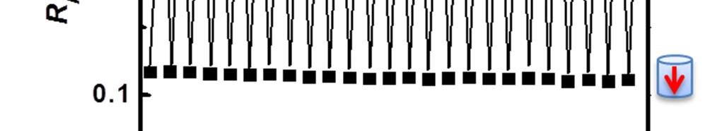
6 wide Ta electrode at H l =-0.4 koe. There is thus little dependence of the critical current density on the dot size in this range and the critical current scales with the cross section of the bottom electrode. More insight is obtained when sweeping the magnetic field at constant pulse amplitude. Figure 4 shows the AHE resistance (Fig. 4 (a)) and the TMR signal (Fig. 4 (b)) as a function of H l after the successive injection of a positive (black square) or negative (red dots) current pulse of amplitude I=20 ma (j 7.5x10 11 A/m²) for a dot of 1 µm diameter. At low H l <0.1 koe, no magnetization switching is observed, which shows that neither the external field nor the in-plane component of the stray field from the top layer is sufficient to trigger the magnetization reversal. For 0.1 koe < H l <0.7 koe, current induced magnetization switching occurs: the injection of positive (resp. negative) current pulse leads to the reversal of the bottom FeCoB layer magnetization along the up (resp. down) direction (AHE signal, Fig.4 (a)). Since the magnetization of the top electrode points upward in this field range due to the perpendicular component of H l, the switching of the bottom FeCoB layer leads to different TMR signals for positive and negative pulses (Fig. 4(b)). For negative magnetic field, switching of the bottom FeCoB layer is also observed but with reversed polarity of current pulses. These experiments can be used to draw a current-field switching diagram constructed using the TMR signal for a 1 µm diameter MTJ dot (Fig. 5(a)). Different behaviors are observed when injecting current pulses depending on the value of j. At low current density j<5x10 11 A/m² (region I), no hysteretic switching is observed, but current injection leads to a reduction of the coercive field of the bottom layer (black open-triangles) with increasing pulse amplitude. This can be understood by the combination of a weak current-induced effect and the residual vertical component of the external field H z, which assists magnetization reversal towards the equilibrium direction, parallel to H z [6]. At higher current density (j>5x10 11 A/m²) 6
7 (region III), current-induced hysteretic switching occurs. The associated j-h l region (III, green) is delimited at low H l by the minimum magnetic field required to trigger the switching and at high H l by the coercive field of the bottom layer due to the perpendicular component of H l. In between these two regions, no antiparallel state is observed (region II, red). In this case, the reversal of the bottom FeCoB layer occurs at the coercive field of the top layer and is promoted by the stray field of the reversed magnetization of the top layer. Note that this switching diagram is similar to the one measured for a single layer [6], except for region II where no change in the TMR signal is observed. We also studied the dependence of the critical current I c on the pulse length τ p for 30 ns<τ p <500 ns (Fig. 5(b), H l =-0.4 koe). We observe that I c scales linearly with 1/τ p for τ p <100 ns. A similar scaling has been reported in Pt/Co/AlO x trilayer [6] down to 400 ps [12]. This result is in contradiction with macrospin simulations, which predict a weak dependence of I c on τ p [12, 13]. Such a scaling is more consistent with a reversal process governed by domain nucleation followed by domain wall (DW) motion, which is expected given the large diameter of the pillar [14]. Assuming that the DW velocity scales linearly with the current density, the critical current required for the DW to traverse the whole pillar is expected to scale as 1/τ p, as observed experimentally. The critical current density for which the magnetization can be reversed back and forth by current pulses with opposite polarities ( 5x10 11 A/m² at 50 ns) is higher compared to j c reported in similar experiments in perpendicularly magnetized Ta/CoFe/MgO [8] (j c =8x10 10 A/m 2 ) and Ta/CoFe/MgO [15] (j c =1x10 10 A/m 2 ) multilayers. This may be accounted for by several features of our experimental scheme. First, we inject short current pulses (50 ns) and use a Si substrate, whereas previous experiments used quasi DC current and Si/SiO 2 substrates, which result in a smaller critical current density due to thermally assisted magnetization reversal. Second, part of the current flows into the arms of the Hall cross which 7
8 leads to a local decrease of the current density below the MTJ dots, resulting in a lower torque [16]. Third, the dipolar field exerted by the top layer and the perpendicular component of the external magnetic field prevent the switching to an antiparallel configuration and thus increase the critical current density for which bipolar switching is observed. A key parameter for the density of the memory is also the writing current that will define the size of the addressing transistor. For j c = 5x10 11 A/m², the large thickness and width of the bottom Ta stripe lead to relatively high critical switching current in our experiments. Assuming that the Slonczewski-like part of the SOT arises mainly from the spin Hall effect [22], the spin current generated by current injection should saturate for Ta layers thicker than the spin diffusion length [26]. This was estimated between to be about 1.8 nm in Ta at room temperature [25]. In addition, the critical current density should remain approximately constant as a function of dot size. Thus, assuming a 3 nm thick 50 nm wide Ta track, a critical current of about 25 µa is expected which is similar to the best results for perpendicular STT-MRAM [17,18,19]. Finally, we note that the longitudinal magnetic bias field can be generated by a set of permanent magnets [9]. In summary, we have fabricated a three-terminal elementary memory cell of a perpendicular SOT-MRAM and demonstrated its basic read and write operations. The SOT- MRAM cell is composed of a perpendicular FeCoB/MgO/FeCoB MTJ with high TMR on top of a Ta track. We have shown that the magnetic bit represented by the relative alignment of the magnetization of the top and bottom FeCoB layers can be reproducibly written by the injection of current pulses in the Ta bottom electrode (5x10 11 A/m², 50 ns-long pulses) and read by measuring the large TMR signal. Our work demonstrates the proof of concept of a perpendicular SOT-MRAM memory cell. 8
9 This work was supported by the European Commission under the Seventh Framework Program (Grant Agreement , spot project). The devices were fabricated at the Plateforme de Technologie Amont (PTA) in Grenoble. 9
10 References [1] J. Hutchby, and M. Garner, Assessment of the Potential and Maturity of Selected Emerging Research Memory Technologies Workshop and ERD/ERM Working Group Meeting, 6 7 April 2010, p. 1 (ITRS Edition) (2010) [2] W. Zhao, E. Belhaire, C. Chappert, and P. Mazoyer, ACM Trans. Embed. Comput. Syst. 9 14:1 14:16 (2009) [3] G. Prenat, M. El Baraji, W. Guo, R. Sousa, L. Buda-Prejbeanu, B. Dieny, V. Javerliac, J.- P. Nozieres, W. Zhao, and E. Belhaire, In 14th IEEE International Conference on Electronics, Circuits and Systems, ICECS, 190 (2007) [4] M. Marins de Castro, R. C. Sousa, S. Bandiera, C. Ducruet, A. Chavent, S. Auffret, C. Papusoi, I.L. Prejbeanu, C. Portemont, L. Vila, U. Ebels, B. Rodmacq, and B. Dieny, J. Appl. Phys. Lett. 111, 07C912 (2012) [5] K.C. Chun, H. Zhao, J. Harms, T.-H. Kim, J.-P. Wang, and C. Kim, IEEE Journal of Solid-State Circuits 48, 598 (2013) [6] I. M. Miron, K. Garello, G. Gaudin, P.-J. Zermatten, M.V. Costache, S. Auffret, S. Bandiera, B. Rodmacq, A. Schuhl, P. Gambardella, Nature 476, 189 (2011) [7] C. O. Avci, K. Garello, I.-M. Miron, G. Gaudin, S. Auffret, O. Boulle, Appl. Phys. Lett., 100, (2011) [8] L. Liu, C. Pai, Y. Li, H. M. Tseng, D.C. Ralph, and R.A. Buhrman, Science 336, 55 (2012) [9] G. Gaudin, I. M. Miron, P. Gambardella, A. Schuhl, Magnetic memory element, Patent, US Patent application, 12/899,072, 12/899,091,12/959980, (2010) 10
11 [10] M. Yamanouchi, L. Chen, J. Kim, M. Hayashi, H. Sato, S. Fukami, S. Ikeda, F. Matsukura, H. Ohno, Appl. Phys. Lett. 102, (2013) [11] C. Pai, L. Liu, Y. Li, H. M. Tseng, D.C. Ralph, and R.A. Buhrman, Appl. Phys. Lett. 101, (2012) [12] K. Garello, C.O. Avci, I.M. Miron, O. Boulle, S. Auffret, P. Gambardella and G. Gaudin, arxiv: (2013) [13] K.-S. Lee, S.-W. Lee, B.-C. Min and, K.-J. Lee, Appl. Phys. Lett., 102, (2013) [14] G. Finocchio, M. Carpentieri, E. Martinez, B. Azzerboni, Appl. Phys. Lett. 102, (2013) [15] S. Emori, U. Bauer, S-M. Ahn, E. Martinez, and G. S. D. Beach. Nat. Mater., 12, 611 (2013) [16] K. Garello, I. M. Miron, C. O. Avci, F. Freimuth, Y. Mokrousov, S. Blügel, S. Auffret, O. Boulle, G. Gaudin, P.Gambardella, Nat. Nano., 8, 587 (2013) [17] K. Yamane, Y. Higo, H. Uchida, Y. Nanba, S. Sasaki, H. Ohmori, K. Bessho and M. Hosomi, IEEE Transactions on Magnetics 49 (7), (2013) [18] G. Jan, Y-J. Wang, T. Moriyama, Y-J Lee, M. Lin, T. Zhong, R-Y. Tong, T. Torng, P-K. Wang, Appl. Phys. Exp., 5, (2012) [19] M. Gajek, J. J. Nowak, J. Z. Sun, P. L. Trouilloud, E. J. O Sullivan, D. W. Abraham, M. C. Gaidis, G. Hu, S. Brown, Y. Zhu, R. P. Robertazzi, W. J. Gallagher and D. C. Worledge, Appl. Phys. Lett, 100, (2012 ) 11
12 [20] P.M. Haney, H.-W. Lee, K.-J. Lee, A. Manchon and M.D. Stiles, Phys. Rev. B 87, (2013) [21] F. Freimuth, S. Blugel, Y. Mokrousov, arxiv: (2013) [22] P.M. Haney, H.-W. Lee, K.-J. Lee, A. Manchon and M.D Stiles, arxiv: (2013) [23] W.S. Zhao, Y. Zhang, T. Devolder, J.O. Klein, D. Ravelosona, C. Chappert, P. Mazoyer, Microelectronics Reliability, 52, (2012) [24] G. Panagopoulos, C. Augustine, K. Roy, In: Proc in device research conference (DRC) p (2011) [25] C. Hahn, G. de Loubens, O. Klein, and M. Viret, V. V. Naletov, J. Ben Youssef, Phys. Rev. B, 87, (2013) [26] L. Liu, T. Moriyama, D. C. Ralph, and R. A. Buhrman, Phys. Rev. Lett., 106, (2011) [27] N. S. Kim, T. Austin, D. Baauw, T. Mudge, IEEE Computer Society, pp (2003) [28] M. H. Kryder and C. Soo Kim, IEEE Transactions on magnetics, 45, 10 (2009) 12
13 Figure Captions: Fig.1 (a) Illustration of a three-terminal MTJ with a Hall cross geometry. The black (blue) up and red (yellow) down arrows indicate the equilibrium magnetization states of the bottom (top) FeCoB layers. (b) Scanning electron microscopy of a 1µm dot diameter patterned MTJ on top a 1.3µm wide Ta electrode with a schematic representation of the electrical measurement setup., and represent the two terminals for the Hall voltage and MTJ voltage measurements respectively. Fig. 2 (a) TMR as a function of the perpendicular magnetic field for 1µm dot diameter. The black and red curves show respectively a major and a minor loop. (b) TMR as a function of current pulse amplitude I p injected in the Ta electrode using 50 ns long pulses under an inplane magnetic field H l =-0.4 koe. The arrows show the sweep direction of I p. Fig. 3 (a) Schematic of the pulse sequence. (b) The AHE resistance (proportional to the M z component of the bottom FeCoB layer) and (c) TMR measured after the injection of positive (black squares) and negative (red circles) current pulses of amplitude I p =20 ma and 50 ns long under H l =-0.4 koe. Fig. 4 (a) The AHE resistance and (b) TMR as a function of H l measured after the injection of positive (black squares) and negative current pulses (red circles) of amplitude I p =20 ma and a length of 50 ns. The dot diameter is 1µm. H l is swept from negative to positive magnetic fields. Fig. 5 (a) I P -H l switching diagram constructed from the measurement of the TMR signal for a 1 µm diameter MTJ (50 ns long pulses). Region I: current assisted magnetization reversal. The open black up-triangles and the dotted line indicate the coercive field of the bottom and 13
14 top FeCoB layers respectively. Region II: low TMR signal (parallel alignment). Region III: Current-induced magnetization switching. The red squares and the blue circles indicate the maximum field and minimum field at which current induced magnetization switching of the bottom layer is observed. and indicate the parallel state where both FeCoB magnetizations are oriented upward and downward respectively. (b) Dependence of the critical current j c on the inverse pulse width (1/ p ). The black line is a guide for the eyes. 14
15 Fig.1 Fig.2 15


16 Fig.3 16
17 Fig.4 Fig.5 17
Current-driven Magnetization Reversal in a Ferromagnetic Semiconductor. (Ga,Mn)As/GaAs/(Ga,Mn)As Tunnel Junction
As/GaAs/(Ga,Mn)As Tunnel Junction") Current-driven Magnetization Reversal in a Ferromagnetic Semiconductor (Ga,Mn)As/GaAs/(Ga,Mn)As Tunnel Junction D. Chiba 1, 2*, Y. Sato 1, T. Kita 2, 1, F. Matsukura 1, 2, and H. Ohno 1, 2 1 Laboratory
Current-driven Magnetization Reversal in a Ferromagnetic Semiconductor (Ga,Mn)As/GaAs/(Ga,Mn)As Tunnel Junction D. Chiba 1, 2*, Y. Sato 1, T. Kita 2, 1, F. Matsukura 1, 2, and H. Ohno 1, 2 1 Laboratory
Two-terminal spin orbit torque magnetoresistive random access memory
 Two-terminal spin orbit torque magnetoresistive random access memory Noriyuki Sato 1, Fen Xue 1,3, Robert M. White 1,2, Chong Bi 1, and Shan X. Wang 1,2,* 1 Stanford University, Department of Electrical
0.002 ( ) R xy
 R xy") a b z 0.002 x H y R xy () 0.000-0.002 0 90 180 270 360 (degree) Supplementary Figure 1. Planar Hall effect resistance as a function of the angle of an in-plane field. a, Schematic of the planar Hall resistance
a b z 0.002 x H y R xy () 0.000-0.002 0 90 180 270 360 (degree) Supplementary Figure 1. Planar Hall effect resistance as a function of the angle of an in-plane field. a, Schematic of the planar Hall resistance
arxiv: v1 [cond-mat.mtrl-sci] 28 Jul 2008
![arxiv: v1 [cond-mat.mtrl-sci] 28 Jul 2008](/thumbs/88/117898456.jpg "arxiv: v1 [cond-mat.mtrl-sci] 28 Jul 2008") Current induced resistance change of magnetic tunnel junctions with ultra-thin MgO tunnel barriers Patryk Krzysteczko, 1, Xinli Kou, 2 Karsten Rott, 1 Andy Thomas, 1 and Günter Reiss 1 1 Bielefeld University,
Current induced resistance change of magnetic tunnel junctions with ultra-thin MgO tunnel barriers Patryk Krzysteczko, 1, Xinli Kou, 2 Karsten Rott, 1 Andy Thomas, 1 and Günter Reiss 1 1 Bielefeld University,
Current-induced four-state magnetization switching by spin-orbit torques in. perpendicular ferromagnetic trilayers
 Current-induced four-state magnetization switching by spin-orbit torques in perpendicular ferromagnetic trilayers Y. Sheng, 1,2 Y. C. Li, 2,3 X. Q. Ma, 1 K. Y. Wang 2,3,4 1 Department of Physics, University
Spin-orbit torque in Pt/CoNiCo/Pt symmetric devices
 Spin-orbit torque in Pt/CoNiCo/Pt symmetric devices Meiyin Yang 1, Kaiming Cai 1, Hailang Ju 2, Kevin William Edmonds 3, Guang Yang 4, Shuai Liu 2, Baohe Li 2, Bao Zhang 1, Yu Sheng 1, ShouguoWang 4, Yang
Analytical expression for the harmonic Hall voltages in evaluating spin orbit torques
 Analytical expression for the harmonic all voltages in evaluating spin orbit torques Masamitsu ayashi National Institute for Materials Science, Tsukuba 35-47, Japan Solid understanding of current induced
Anisotropic Current-Controlled Magnetization Reversal in the Ferromagnetic Semiconductor (Ga,Mn)As
As") Anisotropic Current-Controlled Magnetization Reversal in the Ferromagnetic Semiconductor (Ga,Mn)As Yuanyuan Li 1, Y. F. Cao 1, G. N. Wei 1, Yanyong Li 1, Y. i and K. Y. Wang 1,* 1 SKLSM, Institute of Semiconductors,
Anisotropic Current-Controlled Magnetization Reversal in the Ferromagnetic Semiconductor (Ga,Mn)As Yuanyuan Li 1, Y. F. Cao 1, G. N. Wei 1, Yanyong Li 1, Y. i and K. Y. Wang 1,* 1 SKLSM, Institute of Semiconductors,
SUPPLEMENTARY INFORMATION
 Spin-orbit torque magnetization switching controlled by geometry C.K.Safeer, Emilie Jué, Alexandre Lopez, Liliana Buda-Prejbeanu, Stéphane Auffret, Stefania Pizzini, Olivier Boulle, Ioan Mihai Miron, Gilles
Tailoring the magnetic anisotropy of CoFeB/MgO stacks onto W with a Ta buffer layer
 Tailoring the magnetic anisotropy of CoFeB/MgO stacks onto W with a Ta buffer layer Andreas Kaidatzis, Cristina Bran, Vasilios Psycharis, Manuel Vázquez, José Miguel García-Martín, and Dimitrios Niarchos
Spin-transfer-torque efficiency enhanced by edge-damage. of perpendicular magnetic random access memories
 Spin-transfer-torque efficiency enhanced by edge-damage of perpendicular magnetic random access memories Kyungmi Song 1 and Kyung-Jin Lee 1,2,* 1 KU-KIST Graduate School of Converging Science and Technology,
Magnetic oscillations driven by the spin Hall effect in 3-terminal magnetic tunnel junction. devices. Cornell University, Ithaca, NY 14853
 Magnetic oscillations driven by the spin Hall ect in 3-terminal magnetic tunnel junction devices Luqiao Liu 1, Chi-Feng Pai 1, D. C. Ralph 1,2, R. A. Buhrman 1 1 Cornell University, Ithaca, NY 14853 2
Focused-ion-beam milling based nanostencil mask fabrication for spin transfer torque studies. Güntherodt
 Focused-ion-beam milling based nanostencil mask fabrication for spin transfer torque studies B. Özyilmaz a, G. Richter, N. Müsgens, M. Fraune, M. Hawraneck, B. Beschoten b, and G. Güntherodt Physikalisches
Perpendicular MTJ stack development for STT MRAM on Endura PVD platform
 Perpendicular MTJ stack development for STT MRAM on Endura PVD platform Mahendra Pakala, Silicon Systems Group, AMAT Dec 16 th, 2014 AVS 2014 *All data in presentation is internal Applied generated data
Effect of heavy metal layer thickness on spin-orbit torque and current-induced. switching in Hf CoFeB MgO structures 90095, USA USA.
 Effect of heavy metal layer thickness on spin-orbit torque and current-induced switching in Hf CoFeB MgO structures Mustafa Akyol, 1, 2 Wanjun Jiang, 3 Guoqiang Yu, 1 Yabin Fan, 1 Mustafa Gunes, 4 Ahmet
Room-temperature perpendicular magnetization switching through giant spin-orbit torque from sputtered Bi x Se (1-x) topological insulator material
 topological insulator material") Room-temperature perpendicular magnetization switching through giant spin-orbit torque from sputtered Bi x Se (1-x) topological insulator material Mahendra DC 1, Mahdi Jamali 2, Jun-Yang Chen 2, Danielle
Room-temperature perpendicular magnetization switching through giant spin-orbit torque from sputtered Bi x Se (1-x) topological insulator material Mahendra DC 1, Mahdi Jamali 2, Jun-Yang Chen 2, Danielle
Adjustable current-induced magnetization switching. utilizing interlayer exchange coupling
 Adjustable current-induced magnetization switching utilizing interlayer exchange coupling Yu Sheng, Kevin William Edmonds, Xingqiao Ma, Houzhi Zheng and Kaiyou Wang* Prof. K. Wang, Prof. H. Zheng State
Quantitative characterization of spin-orbit torques in Pt/Co/Pt /Co/Ta/BTO heterostructure on the magnetization azimuthal angle dependence
 Quantitative characterization of spin-orbit torques in Pt/Co/Pt /Co/Ta/BTO heterostructure on the magnetization azimuthal angle dependence Christian Engel, Sarjoosing Goolaup, Feilong Luo, and Wen Siang
S. Mangin 1, Y. Henry 2, D. Ravelosona 3, J.A. Katine 4, and S. Moyerman 5, I. Tudosa 5, E. E. Fullerton 5
 Spin transfer torques in high anisotropy magnetic nanostructures S. Mangin 1, Y. enry 2, D. Ravelosona 3, J.A. Katine 4, and S. Moyerman 5, I. Tudosa 5, E. E. Fullerton 5 1) Laboratoire de Physique des
An Overview of Spin-based Integrated Circuits
 ASP-DAC 2014 An Overview of Spin-based Integrated Circuits Wang Kang, Weisheng Zhao, Zhaohao Wang, Jacques-Olivier Klein, Yue Zhang, Djaafar Chabi, Youguang Zhang, Dafiné Ravelosona, and Claude Chappert
Enhancement of Perpendicular Magnetic Anisotropy and Transmission of
 Enhancement of Perpendicular Magnetic Anisotropy and Transmission of Spin-all-Effect-Induced Spin Currents by a f Spacer ayer in W/f/CoFeB/MgO ayer Structures Chi-Feng Pai, 1 Minh-ai Nguyen, 1 Carina Belvin,
Current-induced switching in a magnetic insulator
 In the format provided by the authors and unedited. DOI: 10.1038/NMAT4812 Current-induced switching in a magnetic insulator Can Onur Avci, Andy Quindeau, Chi-Feng Pai 1, Maxwell Mann, Lucas Caretta, Astera
Gate voltage modulation of spin-hall-torque-driven magnetic switching. Cornell University, Ithaca, NY 14853
 Gate voltage modulation of spin-hall-torque-driven magnetic switching Luqiao Liu 1, Chi-Feng Pai 1, D. C. Ralph 1,2 and R. A. Buhrman 1 1 Cornell University, Ithaca, NY 14853 2 Kavli Institute at Cornell,
Optical studies of current-induced magnetization
 Optical studies of current-induced magnetization Virginia (Gina) Lorenz Department of Physics, University of Illinois at Urbana-Champaign PHYS403, December 5, 2017 The scaling of electronics John Bardeen,
IEEE TRANSACTIONS ON ELECTRON DEVICES, VOL. 63, NO. 11, NOVEMBER
 IEEE TRANSACTIONS ON ELECTRON DEVICES, VOL. 63, NO. 11, NOVEMBER 2016 4499 All-Spin-Orbit Switching of Perpendicular Magnetization Mohammad Kazemi, Student Member, IEEE, Graham E. Rowlands, Shengjie Shi,
Spin Hall Switching of the Magnetization in Ta/TbFeCo Structures with Bulk. Perpendicular Anisotropy
 Spin Hall Switching of the Magnetization in Ta/TbFeCo Structures with Bulk Perpendicular Anisotropy Zhengyang Zhao, Mahdi Jamali, Angeline Klemm, and Jian-Ping Wang * Department of Electrical and Computer
SUPPLEMENTARY INFORMATION
 SUPPLEMENTARY INFORMATION doi:.38/nphys436 Non-adiabatic spin-torques in narrow magnetic domain walls C. Burrowes,2, A. P. Mihai 3,4, D. Ravelosona,2, J.-V. Kim,2, C. Chappert,2, L. Vila 3,4, A. Marty
SPICE Modeling of STT-RAM for Resilient Design. Zihan Xu, Ketul Sutaria, Chengen Yang, Chaitali Chakrabarti, Yu (Kevin) Cao School of ECEE, ASU
 Cao School of ECEE, ASU") SPICE odeling of STT-RA for Resilient Design Zihan Xu, Ketul Sutaria, Chengen Yang, Chaitali Chakrabarti, Yu (Kevin) Cao School of ECEE, ASU OUTLINE - 2 - Heterogeneous emory Design A Promising Candidate:
SPICE odeling of STT-RA for Resilient Design Zihan Xu, Ketul Sutaria, Chengen Yang, Chaitali Chakrabarti, Yu (Kevin) Cao School of ECEE, ASU OUTLINE - 2 - Heterogeneous emory Design A Promising Candidate:
Spin-Orbit Torques in ferrimagnetic GdFeCo Alloys
 Spin-Orbit Torques in ferrimagnetic GdFeCo Alloys Niklas Roschewsky, Tomoya Matsumura, Suraj Cheema, 3 Frances Hellman,, 4 Takeshi Kato, Satoshi Iwata, 5 4, 6, and Sayeef Salahuddin Department of Physics,
Switching Properties in Magnetic Tunnel Junctions with Interfacial Perpendicular Anisotropy: Micromagnetic Study
 1 Switching Properties in Magnetic Tunnel Junctions with Interfacial Perpendicular Anisotropy: Micromagnetic Study R. Tomasello 1, V. Puliafito 2, B. Azzerboni 2, G. Finocchio 2 1 Department of Computer
Quantitative characterization of the spin orbit torque using harmonic Hall voltage measurements
 Quantitative characterization of the spin orbit torque using harmonic all voltage measurements Masamitsu ayashi and Junyeon Kim National Institute for Materials Science, Tsukuba 35-47, Japan Michihiko
Magnetic bubblecade memory based on chiral domain walls
 Magnetic bubblecade memory based on chiral domain walls Kyoung-Woong Moon, Duck-Ho Kim, Sang-Cheol Yoo, Soong-Geun Je, Byong Sun Chun, Wondong Kim, Byoung-Chul Min, Chanyong Hwang & Sug-Bong Choe 1. Sample
Spin orbit torque driven magnetic switching and memory. Debanjan Bhowmik
 Spin orbit torque driven magnetic switching and memory Debanjan Bhowmik Spin Transfer Torque Fixed Layer Free Layer Fixed Layer Free Layer Current coming out of the fixed layer (F2) is spin polarized in
Supplementary Figure 1. Magnetic domain configuration under out-of-plane field application. (a), (b) MTXM images showing magnetic domain state
, (b) MTXM images showing magnetic domain state") Supplementary Figure 1. Magnetic domain configuration under out-of-plane field application. (a), (b) MTXM images showing magnetic domain state acquired at a given out-ofplane magnetic field. Bright and
Supplementary Figure 1. Magnetic domain configuration under out-of-plane field application. (a), (b) MTXM images showing magnetic domain state acquired at a given out-ofplane magnetic field. Bright and
This document is an author-formatted work. The definitive version for citation appears as:
 This document is an author-formatted work. The definitive version for citation appears as: A. Roohi, R. Zand, D. Fan and R. F. DeMara, "Voltage-based Concatenatable Full Adder using Spin Hall Effect Switching,"
Lecture 6 NEW TYPES OF MEMORY
 Lecture 6 NEW TYPES OF MEMORY Memory Logic needs memory to function (efficiently) Current memories Volatile memory SRAM DRAM Non-volatile memory (Flash) Emerging memories Phase-change memory STT-MRAM (Ferroelectric
Page 1. A portion of this study was supported by NEDO.
 MRAM : Materials and Devices Current-induced Domain Wall Motion High-speed MRAM N. Ishiwata NEC Corporation Page 1 A portion of this study was supported by NEDO. Outline Introduction Positioning and direction
Spin transfer torque devices utilizing the giant spin Hall effect of tungsten
 Spin transfer torque devices utilizing the giant spin Hall effect of tungsten Chi-Feng Pai, 1,a) Luqiao Liu, 1 Y. Li, 1 H. W. Tseng, 1 D. C. Ralph 1,2 and R. A. Buhrman 1 1 Cornell University, Ithaca,
A Perpendicular Spin Torque Switching based MRAM for the 28 nm Technology Node
 A Perpendicular Spin Torque Switching based MRAM for the 28 nm Technology Node U.K. Klostermann 1, M. Angerbauer 1, U. Grüning 1, F. Kreupl 1, M. Rührig 2, F. Dahmani 3, M. Kund 1, G. Müller 1 1 Qimonda
Time resolved transport studies of magnetization reversal in orthogonal spin transfer magnetic tunnel junction devices
 Invited Paper Time resolved transport studies of magnetization reversal in orthogonal spin transfer magnetic tunnel junction devices Georg Wolf a, Gabriel Chaves-O Flynn a, Andrew D. Kent a, Bartek Kardasz
Ultrafast switching of a nanomagnet by a combined out-of-plane and in-plane polarized spin-current pulse
 Ultrafast switching of a nanomagnet by a combined out-of-plane and in-plane polarized spin-current pulse O. J. Lee, V. S. Pribiag, P. M. Braganca, P. G. Gowtham, D. C. Ralph and R. A. Buhrman Cornell University,
Wouldn t it be great if
 IDEMA DISKCON Asia-Pacific 2009 Spin Torque MRAM with Perpendicular Magnetisation: A Scalable Path for Ultra-high Density Non-volatile Memory Dr. Randall Law Data Storage Institute Agency for Science Technology
Room temperature spin-orbit torque switching induced by a
 Room temperature spin-orbit torque switching induced by a topological insulator Jiahao Han 1, A. Richardella 2, Saima Siddiqui 1, Joseph Finley 1, N. Samarth 2 and Luqiao Liu 1* 1 Department of Electrical
Nonvolatile CMOS Circuits Using Magnetic Tunnel Junction
 November 3-4, 2011 Berkeley, CA, USA Nonvolatile CMOS Circuits Using Magnetic Tunnel Junction Hideo Ohno 1,2 1 Center for Spintronics Integrated Systems, Tohoku University, Japan 2 Laboratory for Nanoelectronics
Spin-transfer switching and thermal stability in an FePt/Au/FePt nanopillar prepared by alternate monatomic layer deposition
 Spin-transfer switching and thermal stability in an FePt/Au/FePt nanopillar prepared by alternate monatomic layer deposition Kay Yakushiji, Shinji Yuasa, Taro Nagahama, Akio Fukushima, Hitoshi Kubota,
Saroj P. Dash. Chalmers University of Technology. Göteborg, Sweden. Microtechnology and Nanoscience-MC2
 Silicon Spintronics Saroj P. Dash Chalmers University of Technology Microtechnology and Nanoscience-MC2 Göteborg, Sweden Acknowledgement Nth Netherlands University of Technology Sweden Mr. A. Dankert Dr.
From Spin Torque Random Access Memory to Spintronic Memristor. Xiaobin Wang Seagate Technology
 From Spin Torque Random Access Memory to Spintronic Memristor Xiaobin Wang Seagate Technology Contents Spin Torque Random Access Memory: dynamics characterization, device scale down challenges and opportunities
External-Field-Free Spin Hall Switching of Perpendicular Magnetic Nanopillar with a Dipole-Coupled Composite Structure
 External-Field-Free Spin Hall Switching of Perpendicular Magnetic Nanopillar with a Dipole-Coupled Composite Structure Zhengyang Zhao, Angeline K. Smith, Mahdi Jamali, and Jian-Ping Wang * Department of
Magnetization Dynamics in Spintronic Structures and Devices
 Japanese Journal of Applied Physics Vol. 45, No. 5A, 2006, pp. 3835 3841 #2006 The Japan Society of Applied Physics Magnetization Dynamics in Spintronic Structures and Devices Structure, Materials and
MAGNETO-RESISTANCE AND INDUCED DOMAIN STRUCTURE IN TUNNEL JUNCTIONS
 Mat. Res. Soc. Symp. Proc. Vol. 674 001 Materials Research Society MAGNETO-RESISTANCE AND INDUCED DOMAIN STRUCTURE IN TUNNEL JUNCTIONS M. Hehn, O. Lenoble, D. Lacour and A. Schuhl Laboratoire de Physique
Resonance Measurement of Nonlocal Spin Torque in a Three-Terminal Magnetic Device
 Resonance Measurement of Nonlocal Spin Torque in a Three-Terminal Magnetic Device Lin Xue 1, Chen Wang 1, Yong-Tao Cui 1, Luqiao Liu 1, A. Swander 1, J. Z. Sun 3, R. A. Buhrman 1 and D. C. Ralph 1,2 1
Planar Hall Effect Based Characterization of Spin Orbital Torques in Ta/CoFeB/MgO Structures
 Planar Hall Effect Based Characterization of Spin Orbital Torques in Ta/CoFeB/MgO Structures Mahdi Jamali 1, Zhengyang Zhao 1, Mahendra DC 2, Delin Zhang 1, Hongshi Li 3, Angeline K. Smith 1, Jian-Ping
Planar Hall Effect in Magnetite (100) Films
 Films") Planar Hall Effect in Magnetite (100) Films Xuesong Jin, Rafael Ramos*, Y. Zhou, C. McEvoy and I.V. Shvets SFI Nanoscience Laboratories, School of Physics, Trinity College Dublin, Dublin 2, Ireland 1 Abstract.
Planar Hall Effect in Magnetite (100) Films Xuesong Jin, Rafael Ramos*, Y. Zhou, C. McEvoy and I.V. Shvets SFI Nanoscience Laboratories, School of Physics, Trinity College Dublin, Dublin 2, Ireland 1 Abstract.
MRAM: Device Basics and Emerging Technologies
 MRAM: Device Basics and Emerging Technologies Matthew R. Pufall National Institute of Standards and Technology 325 Broadway, Boulder CO 80305-3337 Phone: +1-303-497-5206 FAX: +1-303-497-7364 E-mail: pufall@boulder.nist.gov
Highly thermally stable sub-20nm magnetic random-access memory based on perpendicular shape anisotropy
 Highly thermally stable sub-20nm magnetic random-access memory based on perpendicular shape anisotropy N. Perrissin 1, S. Lequeux 1, N. Strelkov 1,2, L. Vila 1, L. Buda-Prejbeanu 1, S. Auffret 1, R.C.
Field-free switching of perpendicular magnetic tunnel junction by the interplay
 Field-free switching of perpendicular magnetic tunnel junction by the interplay of spin orbit and spin transfer torques Mengxing Wang 1, Wenlong Cai 1, Daoqian Zhu 1, Jimmy Kan 2, Zhengyang Zhao 3, Kaihua
Advanced Lab Course. Tunneling Magneto Resistance
 Advanced Lab Course Tunneling Magneto Resistance M06 As of: 015-04-01 Aim: Measurement of tunneling magnetoresistance for different sample sizes and recording the TMR in dependency on the voltage. Content
SPIN TRANSFER TORQUES IN HIGH ANISOTROPY MAGNETIC NANOSTRUCTURES
 CRR Report Number 29, Winter 2008 SPIN TRANSFER TORQUES IN HIGH ANISOTROPY AGNETIC NANOSTRUCTURES Eric Fullerton 1, Jordan Katine 2, Stephane angin 3, Yves Henry 4, Dafine Ravelosona 5, 1 University of
Non-uniform switching of the perpendicular magnetization in a spin-torque driven magnetic nanopillar
 SLAC-PUB-14453 Non-uniform switching of the perpendicular magnetization in a spin-torque driven magnetic nanopillar David P. Bernstein, Björn Bräuer, Roopali Kukreja, and Joachim Stöhr Stanford Institute
Programmable Spin Logic Based on Spin Hall Effect in a Single Device
 www.advancedsciencenews.com Programmable Spin Logic Based on Spin Hall Effect in a Single Device Caihua Wan, Xuan Zhang, Zhonghui Yuan, Chi Fang, Wenjie Kong, Qintong Zhang, Hao Wu, Usman Khan, and Xiufeng
MSE 7025 Magnetic Materials (and Spintronics)
") MSE 7025 Magnetic Materials (and Spintronics) Lecture 14: Spin Transfer Torque And the future of spintronics research Chi-Feng Pai cfpai@ntu.edu.tw Course Outline Time Table Week Date Lecture 1 Feb 24
MSE 7025 Magnetic Materials (and Spintronics) Lecture 14: Spin Transfer Torque And the future of spintronics research Chi-Feng Pai cfpai@ntu.edu.tw Course Outline Time Table Week Date Lecture 1 Feb 24
MSE 7025 Magnetic Materials (and Spintronics)
") MSE 7025 Magnetic Materials (and Spintronics) Lecture 1: Introduction Chi-Feng Pai cfpai@ntu.edu.tw Course Outline Magnetism and Magnetic Materials What is magnetism? What is its origin? Magnetic properties
MSE 7025 Magnetic Materials (and Spintronics) Lecture 1: Introduction Chi-Feng Pai cfpai@ntu.edu.tw Course Outline Magnetism and Magnetic Materials What is magnetism? What is its origin? Magnetic properties
arxiv:cond-mat/ v1 4 Oct 2002
 Current induced spin wave excitations in a single ferromagnetic layer Y. Ji and C. L. Chien Department of Physics and Astronomy, The Johns Hopkins University, Baltimore, Maryland arxiv:cond-mat/0210116v1
SUPPLEMENTARY INFORMATION
 SUPPLEMENTARY INFORMATION DOI: 10.1038/NNANO.2013.145 Symmetry magnitude of spin-orbit torques in ferromagnetic heterostructures Kevin Garello, Ioan Mihai Miron, Can Onur Avci, Frank Freimuth, Yuriy Mokrousov,
Low Energy Spin Transfer Torque RAM (STT-RAM / SPRAM) Zach Foresta April 23, 2009
 Zach Foresta April 23, 2009") Low Energy Spin Transfer Torque RAM (STT-RAM / SPRAM) Zach Foresta April 23, 2009 Overview Background A brief history GMR and why it occurs TMR structure What is spin transfer? A novel device A future
Low Energy Spin Transfer Torque RAM (STT-RAM / SPRAM) Zach Foresta April 23, 2009 Overview Background A brief history GMR and why it occurs TMR structure What is spin transfer? A novel device A future
Magneto-Seebeck effect in spin-valve with in-plane thermal gradient
 Magneto-Seebeck effect in spin-valve with in-plane thermal gradient S. Jain 1, a), D. D. Lam 2, b), A. Bose 1, c), H. Sharma 3, d), V. R. Palkar 1, e), C. V. Tomy 3, f), Y. Suzuki 2, g) 1, h) and A. A.
Spin Hall effect clocking of nanomagnetic logic without a magnetic field
 SUPPLEMENTARY INFORMATION DOI: 10.1038/NNANO.2013.241 Spin Hall effect clocking of nanomagnetic logic without a magnetic field (Debanjan Bhowmik *, Long You *, Sayeef Salahuddin) Supplementary Section
Effect of Proton Irradiation on the Magnetic Properties of Antiferromagnet/ferromagnet Structures
 Journal of Magnetics 21(2), 159-163 (2016) ISSN (Print) 1226-1750 ISSN (Online) 2233-6656 http://dx.doi.org/10.4283/jmag.2016.21.2.159 Effect of Proton Irradiation on the Magnetic Properties of Antiferromagnet/ferromagnet
A Technology-Agnostic MTJ SPICE Model with User-Defined Dimensions for STT-MRAM Scalability Studies
 A Technology-Agnostic MTJ SPICE Model with User-Defined Dimensions for STT-MRAM Scalability Studies Model download website: mtj.umn.edu Jongyeon Kim 1, An Chen 2, Behtash Behin-Aein 2, Saurabh Kumar 1,
MODELING OF THE ADVANCED SPIN TRANSFER TORQUE MEMORY: MACRO- AND MICROMAGNETIC SIMULATIONS
 MODELING OF THE ADVANCED SPIN TRANSFER TORQUE MEMORY: MACRO- AND MICROMAGNETIC SIMULATIONS Alexander Makarov, Viktor Sverdlov, Dmitry Osintsev, Josef Weinbub, and Siegfried Selberherr Institute for Microelectronics
Magnon-drag thermopile
 Magnon-drag thermopile I. DEVICE FABRICATION AND CHARACTERIZATION Our devices consist of a large number of pairs of permalloy (NiFe) wires (30 nm wide, 20 nm thick and 5 µm long) connected in a zigzag
SUPPLEMENTARY INFORMATION
 SUPPLEMENTARY INFORMATION doi:10.1038/nature11733 1 Ising-Macrospin model The Ising-Macrospin (IM) model simulates the configuration of the superlattice (SL) by assuming every layer is a single spin (macrospin)
Supplementary material for : Spindomain-wall transfer induced domain. perpendicular current injection. 1 ave A. Fresnel, Palaiseau, France
 SUPPLEMENTARY INFORMATION Vertical-current-induced Supplementary material for : Spindomain-wall transfer induced domain motion wallin MgO-based motion in MgO-based magnetic magnetic tunnel tunneljunctions
ANGULAR DEPENDENCE OF MAGNETIC PROPERTIES IN Co/Pt MULTILAYERS WITH PERPENDICULAR MAGNETIC ANISOTROPY
 International Journal of Modern Physics B Vol. 19, Nos. 15, 16 & 17 (2005) 2562-2567 World Scientific Publishing Company World Scientific V www.worldscientific.com ANGULAR DEPENDENCE OF MAGNETIC PROPERTIES
Stability phase diagram of a perpendicular magnetic tunnel junction in noncollinear geometry
 Stability phase diagram of a perpendicular magnetic tunnel junction in noncollinear geometry N. Strelkov, A. Timopheev, R. C. Sousa, M. Chshiev, L. D. Buda-Prejbeanu, B. Dieny To cite this version: N.
Influence of exchange bias on magnetic losses in CoFeB/MgO/CoFeB tunnel junctions
 Influence of exchange bias on magnetic losses in CoFeB/MgO/CoFeB tunnel junctions Ryan Stearrett Ryan Stearrett, W. G. Wang, Xiaoming Kou, J. F. Feng, J. M. D. Coey, J. Q. Xiao, and E. R. Nowak, Physical
Low-power non-volatile spintronic memory: STT-RAM and beyond
 IOP PUBLISHING JOURNAL OF PHYSICS D: APPLIED PHYSICS J. Phys. D: Appl. Phys. 46 (2013) 074003 (10pp) doi:10.1088/0022-3727/46/7/074003 Low-power non-volatile spintronic memory: STT-RAM and beyond K L Wang,
Spin Torque Oscillator from micromagnetic point of view
 Spin Torque Oscillator from micromagnetic point of view Liliana BUDA-PREJBEANU Workshop on Advance Workshop Magnetic on Materials Advance / Cluj-Napoca Magnetic (Romania) Materials 16/9/27 / Cluj-Napoca
Enhanced spin orbit torques by oxygen incorporation in tungsten films
 Enhanced spin orbit torques by oxygen incorporation in tungsten films Timothy Phung IBM Almaden Research Center, San Jose, California, USA 1 Motivation: Memory devices based on spin currents Spin Transfer
arxiv: v1 [physics.app-ph] 1 May 2017
![arxiv: v1 [physics.app-ph] 1 May 2017](/thumbs/72/67272250.jpg "arxiv: v1 [physics.app-ph] 1 May 2017") Magnetic Skyrmions for Cache Memory Mei-Chin Chen 1 and Kaushik Roy 1 1 School of Electrical and Computer Engineering, Purdue University, West Lafayette, 47906, USA * chen1320@purdue.edu ABSTRACT arxiv:1705.01095v1
Magnetic Skyrmions for Cache Memory Mei-Chin Chen 1 and Kaushik Roy 1 1 School of Electrical and Computer Engineering, Purdue University, West Lafayette, 47906, USA * chen1320@purdue.edu ABSTRACT arxiv:1705.01095v1
Interface control of the magnetic chirality in TaN CoFeB MgO heterosctructures
 Interface control of the magnetic chirality in TaN CoFeB MgO heterosctructures Jacob Torrejon 1, Junyeon Kim 1, Jaivardhan Sinha 1, Seiji Mitani 1 and Masamitsu Hayashi 1* 1 National Institute for Materials
New Approaches to Reducing Energy Consumption of MRAM write cycles, Ultra-high efficient writing (Voltage-Control) Spintronics Memory (VoCSM)
 Spintronics Memory (VoCSM)") New Approaches to Reducing Energy Consumption of MRAM write cycles, Ultra-high efficient writing (Voltage-Control) Spintronics Memory (VoCSM) Hiroaki Yoda Corporate Research & Development Center, Toshiba
New Approaches to Reducing Energy Consumption of MRAM write cycles, Ultra-high efficient writing (Voltage-Control) Spintronics Memory (VoCSM) Hiroaki Yoda Corporate Research & Development Center, Toshiba
Fabrication and Measurement of Spin Devices. Purdue Birck Presentation
 Fabrication and Measurement of Spin Devices Zhihong Chen School of Electrical and Computer Engineering Birck Nanotechnology Center, Discovery Park Purdue University Purdue Birck Presentation zhchen@purdue.edu
Mesoscopic Spintronics
 Mesoscopic Spintronics Taro WAKAMURA (Université Paris-Sud) Lecture 1 Today s Topics 1.1 History of Spintronics 1.2 Fudamentals in Spintronics Spin-dependent transport GMR and TMR effect Spin injection
SUPPLEMENTARY INFORMATION
 SUPPLEMENTARY INFORMATION DOI: 10.1038/NNANO.2014.16 Electrical detection of charge current-induced spin polarization due to spin-momentum locking in Bi 2 Se 3 by C.H. Li, O.M.J. van t Erve, J.T. Robinson,
Imprinting domain/spin configurations in antiferromagnets. A way to tailor hysteresis loops in ferromagnetic-antiferromagnetic systems
 Imprinting domain/spin configurations in antiferromagnets A way to tailor hysteresis loops in ferromagnetic-antiferromagnetic systems Dr. J. Sort Institució Catalana de Recerca i Estudis Avançats (ICREA)
Electric-Field-Controlled Magnetoelectric RAM: Progress, Challenges, and Scaling
 IEEE TRANSACTIONS ON MAGNETICS, VOL. 51, NO. 11, NOVEMBER 2015 3401507 Electric-Field-Controlled Magnetoelectric RAM: Progress, Challenges, and Scaling Pedram Khalili Amiri 1,2,JuanG.Alzate 1, Xue Qing
Current-nonlinear Hall effect and spin-orbit torque magnetization. switching in a magnetic topological insulator
 Current-nonlinear Hall effect and spin-orbit torque magnetization switching in a magnetic topological insulator K. Yasuda 1*, A. Tsukazaki 2, R. Yoshimi 3, K. Kondou 3, K. S. Takahashi 3, Y. Otani 3,4,
Symmetry and magnitude of spin-orbit torques in ferromagnetic heterostructures
 1 Symmetry and magnitude of spin-orbit torques in ferromagnetic heterostructures Kevin Garello 1, Ioan Mihai Miron 2, Can Onur Avci 1, Frank Freimuth 3, Yuriy Mokrousov 3, Stefan Blügel 3, Stéphane Auffret
SUPPLEMENTARY INFORMATION
 Magnetization switching through giant spin-orbit torque in a magnetically doped topological insulator heterostructure Yabin Fan, 1,,* Pramey Upadhyaya, 1, Xufeng Kou, 1, Murong Lang, 1 So Takei, 2 Zhenxing
Magnetoresistance due to Domain Walls in Micron Scale Fe Wires. with Stripe Domains arxiv:cond-mat/ v1 [cond-mat.mes-hall] 9 Mar 1998.
![Magnetoresistance due to Domain Walls in Micron Scale Fe Wires. with Stripe Domains arxiv:cond-mat/ v1 [cond-mat.mes-hall] 9 Mar 1998.](/thumbs/90/104152266.jpg "Magnetoresistance due to Domain Walls in Micron Scale Fe Wires. with Stripe Domains arxiv:cond-mat/ v1 [cond-mat.mes-hall] 9 Mar 1998.") Magnetoresistance due to Domain Walls in Micron Scale Fe Wires with Stripe Domains arxiv:cond-mat/9803101v1 [cond-mat.mes-hall] 9 Mar 1998 A. D. Kent a, U. Ruediger a, J. Yu a, S. Zhang a, P. M. Levy a
Magnetoresistance due to Domain Walls in Micron Scale Fe Wires with Stripe Domains arxiv:cond-mat/9803101v1 [cond-mat.mes-hall] 9 Mar 1998 A. D. Kent a, U. Ruediger a, J. Yu a, S. Zhang a, P. M. Levy a
Room temperature chiral magnetic skyrmions in ultrathin Pt/Co/MgO nanostructures
 Room temperature chiral magnetic skyrmions in ultrathin Pt/Co/MgO nanostructures O.Boulle Spintec CEA-INAC / CNRS / Université Grenoble Alpes, Grenoble, France SOCSIS 2016 - Spestses - 29/06/2016 Acknowledgements
Domain wall motions in perpendicularly magnetized CoFe/Pd multilayer
 Domain wall motions in perpendicularly magnetized CoFe/Pd multilayer nanowire Zhaoliang Meng, 1,2 Manoj Kumar, 1 Jinjun Qiu, 2 Guchang Han, 2,* Kie Leong Teo 1,2 and Duc-The Ngo, 3,1,* 1 Department of
Strong Electrical Manipulation of Spin Orbit Torque in Ferromagnetic Heterostructures
 Strong Electrical Manipulation of Spin Orbit Torque in Ferromagnetic Heterostructures Yinuo Yan, Caihua Wan, Xiangjun Zhou, Guoyi Shi, Bin Cui, Jiahao Han, Yihong Fan, Xiufeng Han, Kang L. Wang, Feng Pan,
Critical switching current density induced by spin Hall effect in magnetic structures with firstand second-order perpendicular magnetic anisotropy
 www.nature.com/scientificreports Received: 1 June 017 Accepted: 1 October 017 Published: xx xx xxxx OPEN Critical switching current density induced by spin Hall ect in magnetic structures with firstand
9. Spin Torque Majority Gate
 eyond MOS computing 9. Spin Torque Majority Gate Dmitri Nikonov Thanks to George ourianoff Dmitri.e.nikonov@intel.com 1 Outline Spin majority gate with in-pane magnetization Spin majority gate with perpendicular
An Intrinsic Spin Orbit Torque Nano-Oscillator
 arxiv:188.933v1 [cond-mat.mes-hall] 28 Aug 218 An Intrinsic Spin Orbit Torque Nano-Oscillator M. Haidar, 1 A. A. Awad, 1 M. Dvornik, 1 R. Khymyn, 1 A. Houshang, 1 J. Åkerman 1,2 1 Physics Department, University
Evolution of magnetic domain reversal with temperature in CoÕ Pt multilayers observed by magneto-optical Kerr imaging
 Evolution of magnetic domain reversal with temperature in CoÕ Pt multilayers observed by magneto-optical Kerr imaging X. P. Xie, X. W. Zhao, J. W. Knepper, F. Y. Yang, and R. Sooryakumar Department of
Compact Modeling of STT-RAM and MeRAM A Verilog-A model of Magnetic Tunnel Junction Behavioral Dynamics
 UNIVERSITY OF CALIFORNIA, LOS ANGELES Compact Modeling of STT-RAM and MeRAM A Verilog-A model of Magnetic Tunnel Junction Behavioral Dynamics Dheeraj Srinivasan 3/8/2013 +This work was done under the advisement
Wide range and tunable linear TMR sensor using two exchange pinned electrodes
 Wide range and tunable linear TMR sensor using two change pinned electrodes B. Negulescu a, D. Lacour a, F. Montaigne a, A. Gerken b, J. Paul b, V. Spetter b, J. Marien b, C. Duret c, M. Hehn a a) Institut