Quantum effects in colloidal nanoparticles. From the beauty of single quantum dot physics to ensemble applications...
|
|
|
- Nancy Atkinson
- 6 years ago
- Views:
Transcription
1 Quantum effects in colloidal nanoparticles From the beauty of single quantum dot physics to ensemble applications... Prof Pavlos Lagoudakis Ioffe 10/06/2013


2 Colloidal nanocrystals: nano-engineering low cost chemical synthesis optical tunability through size shape versatility CdSe CdS electron hole hole confined to core, electron spreads over whole length ~16nm nanorods of mixed dimensionality highly polarised luminescence Talapin et al., Nano Letters, 3,

3 Single Particle Spectroscopy 3


4 Single Particle Spectroscopy 10-5 mg/ml 10-6 mg/ml 10-7 mg/ml 10 µm Changing particle concentration 4
5 Manipulate brightness with external electric field V 8 µm 18 nm PL Energy (ev) Integrated Intensity (arb. u.) a) b) E E Electric Field (kv/cm) Manipulating oscillator strength 5
6 Tune photoluminescence energy a) Energy (ev) E b) Electric Field (kv/cm) 2.10 The wave functions are solved iteratively using a finite element method with a sequential optimization of V e,h following the Hartree self-consistent potential approach Muller et al Nano Letters Vol. 5, No Kraus et al Phys. Rev. Lett. 98, Energy (ev) 2.05 E Electric Field (kv/cm) enhanced Quantum Confined Stark Shift (up to 100 mev) at 4K 6
7 Experimental Setup Goal: Control the emission properties with applying an electric field excitation amplifier system 400 nm 5 µj/cm² trigger E-field generator delay spectrometer MCP PL 630 nm CCD glass + ITO SiO (10 nm) Ag (100nm) SiO (10 nm) polystyrene + nanorods (400 nm) 7


 Quadratic Stark")
8 anipulating the wavefunctions in the ensemble 40 V QCSE in ensemble of nanorods E peak (mev) 8 4 E Electric field (MV/cm) Quadratic Stark effect of up to 14 mev 8


9 Gated Photoluminescene laser gate E-Field laser E-Field gate zoom: 10x PL quenching Kraus et al Phys. Rev. Lett. 98, PL burst at room temperature 9
 gate (50 ns) 0 V + - + -")
10 Photoluminescence Quenching and Burst 40 V laser E-Field (1 µs) gate (50 ns) 0 V
 gate 1 µs 100 µs 10 % Kraus et al")

11 Exciton Storage laser E-Field (1 µs 100 µs) gate 1 µs 100 µs 10 % Kraus et al Phys. Rev. Lett. 98, Sufficient exciton storage up to 100 µs! Device! 11
 gate 40 V 10 V Kraus")

12 Burst E-field Dependence laser E-Field (1 µs, 10 V 40 V) gate 40 V 10 V Kraus et al Phys. Rev. Lett. 98, Controlling amount of exciton storage! 12


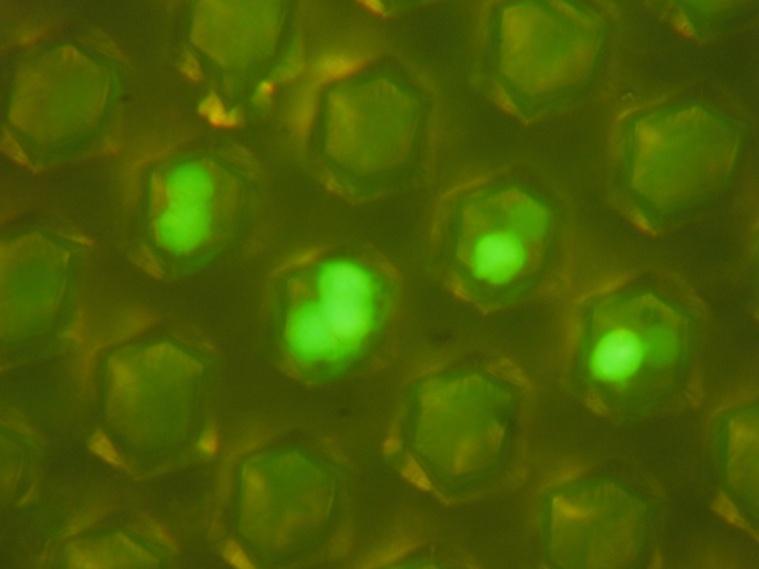
13 The interface to Life Sciences Hi-spots: used by pharmaceuticals Brain 80,000 cell/mm 2 c.a. 161,000 cell/mm 2
14 Neurophotonics V 8 µm 18 nm PL Energy (ev) Voltage (V) 500 Electric field Time (s) Reversely: E-field sensors at the nanoscale 14

15 Controlling alignment of nanocrystal networks 15


 Cellular activity")
16 Controlling alignment of nanocrystal networks PC12 cells Use of nanocrystals underneath the cell layer Seeding of Pc12 cells Li-Niobate substrate Interrogating Neuronal Activity Electrical activity (action potential) Cellular activity (axonal transport) 16


17 Control growth localisation of cells 17

18 Intercepting Neural Signalling (+) Spatial alignment of nanocrystals Interrogating Neuronal Activity Electrical activity (action potential) Cellular activity (axonal transport) Phd project on Neuro/Nano-science Postdoctoral position available School of Physics and Astronomy School of Biological Sciences cell/neuritis-growth Prof Pavlos Lagoudakis 18
19 Intercepting Neural Signalling (+) PC12 cells Seeding of Pc12 cells Li-Niobate substrate Intercepting Neuronal Activity Electrical activity (action potential) Cellular activity (axonal transport) cell/neuritis-growth 19
20 Single mode, single exciton lasing in NQRs From the beauty of single quantum dot physics to ensemble applications...

21 Whispering gallery mode resonators Light confinement inside a microsphere Geometric optic Wave optic Schematic of a spherical microcavity showing distribution and spatial orientation of the mode Rakovich et al., Laser & Photon. Rev. 4, No. 2, (2010)

22 Single-mode single-exciton Laser from quasi-type II Colloidal Quantum Rods Schematic of the experimental arrangement used for demonstration of fiber-coupled laser operation of CdSe/CdS core/shell nanorods in silica microspheres. 22


23 Fabrication procedures flame brushing technique MODIFIED flame brushing technique CLEO 2012 May 6-11, San Jose, California, USA


24 Whispering gallery mode fluorescence 25
25 Single-mode laser emission: INTENSITY (arb. units) CdSe/CdS fluoresence WGM laser emission WAVELENGTH (nm) Laser (black line) and fluorescence emission (red line) spectra from a 9.2-µm-diameter hybrid sphere and the CdSe/CdS nanorods attached to the sphere, respectively. 26
26 Output intensity vs absorbed power: OUTPUT POWER (µw) single-mode laser operation P th = 67.5 µw / η=6.4% ABSORBED PUMP POWER (µw) Laser output power as function of pump power for the single-mode laser operation of a 9.2-µm-large hybrid microsphere. 27
27 Single mode laser Normalized intensity (a. u.) Output power (µw) nanocrystal fluoresence WGM laser emission Wavelength (nm) single-mode laser operation P th = 67.5 µw / η=6.4% Excitation in equatorial zone Microsphere diameter: 9.2 μm Q-factor after the coating 10 5 Laser emission at nm Laser line FWHM: 0.06 nm Lasing threshold: 67.5 μw Maximum output power: 5.5 μw Slope efficiency: 6.4% Absorbed pump power (µw)
28 Multimode laser emission Microsphere diameter: 29.4 μm Normalized intensity (a.u.) nanocrystal fluorescence WGM laser emission Wavelength (nm) Free spectral range The lasing modes distance: 2.4 nm.
29 Tunable laser emission Normalized intensity (a.u) 1.0 IR-laser power: 0 mw (no illumination) mw 40 mw 60 mw Wavelength (nm) Heating of the microsphere with 3.5-µm fs laser (Rep. Rate 80MHz) Shift of laser emission 2.1 nm Temperature variation of the microsphere: Calculation of the tuning range: thermal expansion of the CdSe/CdS nanocrystals thermal expansion of the silica microsphere template thermo-optic coefficient of the nanocrystals change of the CdSe bandgap manuscript submitted to Nature Photonics
30 IR tuning of laser emission: model vs experiment λ (nm) 3.0 microsphere thermal expansion (sim) NQR thermal expansion (sim) 2.5 NQR (dn/dt)-change (sim) band gap-change (sim) 2.0 total contribution (sim) total contribution (exp) IR-LASER POWER (mw) 31
31 Multimode laser emission Normalized intensity (a. u.) nanocrystal fluorescence WGM laser emission biexciton emission single-exciton emission Wavelength (nm) Excitation away from the equatorial zone Second laser line: nm Pump power thresholds of 100 μw and 122 μw


32 Multimode laser emission Intensity (a.u.) single exciton emission biexciton emission Absorbed pump power (µw) Excitation away from the equatorial zone Second laser line: nm Pump power thresholds of 100 μw and 122 μw

33 ħω Em. Abs. Em. Transparenc y Population Inversion Biexciton excitation Biexciton gain mechanism
=ρ h (r)+ρ e (r)")
34 E ħω Em. Δxx: Stark Shift Abs. Stark Shift: Δ ΧΧ =Ε ΧΧ -2Ε Χ Charge density: ρ X (r)=ρ h (r)+ρ e (r) ρ X (r)=e( Ψ h (r) 2 - Ψ e (r) 2 ) Gain
35 Optical gain on CdSe/CdS QRs Length: 27.7±2.2 nm Width: 4.1±0.6 nm electron CdSe CdS E ħω Em. Abs. hole Gain Conduction band offset: ±0.3 ev Valence band offset: 0.78 ev ρ X (r)=e( Ψ h (r) 2 - Ψ e (r) 2 )
36 Exciton dynamics in CdSe/CdS QRs Calculation of the wavefunctions and energies of electrons and holes The calculations have been done in collaboration with Dr. Chunyong Li
37 Exciton dynamics in CdSe/CdS QRs Single Exciton: Ee= ev-- Eh= ev EX=Ee+Eh+Eg=1.972 ev Energy (ev) CB λx= nm 0.3 ev CdSe 7 nm 28 nm ΔE = ev CdS 0.6 ev Biexciton: 2.46 ev Ee1= ev-- Eh1= ev ev 1.68 ev Ee2= eV-- VB Eh2= eV 4.34 nm EXX=Ee1+Eh1+Ee2+Eh2+2*Eg= CdSe CdS ev Stark Shift: ΔXX=Exx-2*Ex= ev λxx= nm CdS single exciton biexciton The calculations have been done in collaboration with Dr. Chunyong Li

38 Optical gain on CdSe/CdS QRs Length: 27.7±2.2 nm Width: 4.1±0.6 nm ħω Em. Abs. E ħω Em. Abs. electron CdSe CdS hole Transparency Gain Conduction band offset: ±0.3 ev Valence band offset: 0.78 ev
39 Hybrid Photonics group the people Dr Caryl Richards Microcavities Ultrafast spectroscopy PhD and post doc positions available Industrial collaborations/acknowledgements: Coherent Inc, IBM-Zurich, Luxtaltek, Leybold, Obducat, TSMC, PhotonSTAR, Q-cells, Solar World, Philips Martin Charlton (ECS, USoton) John Chad (School of Biology, USoton) Pavlos Savvidis (University of Crete) Ian Watson, Martin Dawson (Univ. Strathclyde) Mohamed Henini (University of Nottingham) David Lidzey (The University of Sheffield) Dmitry Talapin (University of Chicago) Horst Weller (University of Hamburg) Andrey Rogach (University of Hong Kong) Alexander Eychmuller, (Uni of Dresden) Jacqueline Bloch and Aristide Lemaître (LPN, Paris) Funding: EU-FP7: ITN-Icarus, ITN-spinoptronics, ITN- Clermont4, N4E NoE. EPSRC: EP/G063494/1, EP/G059268/1, EP/F026455/1, EP/F013876/1 Royal Society Industry in kind contribution: 900k University Southampton: 27k from central funds 40
Nanoscience galore: hybrid and nanoscale photonics
 Nanoscience galore: hybrid and nanoscale photonics Pavlos Lagoudakis SOLAB, 11 June 2013 Hybrid nanophotonics Nanostructures: light harvesting and light emitting devices 2 Hybrid nanophotonics Nanostructures:
Size-Dependent Biexciton Quantum Yields and Carrier Dynamics of Quasi-
 Supporting Information Size-Dependent Biexciton Quantum Yields and Carrier Dynamics of Quasi- Two-Dimensional Core/Shell Nanoplatelets Xuedan Ma, Benjamin T. Diroll, Wooje Cho, Igor Fedin, Richard D. Schaller,
Light Interaction with Small Structures
 Light Interaction with Small Structures Molecules Light scattering due to harmonically driven dipole oscillator Nanoparticles Insulators Rayleigh Scattering (blue sky) Semiconductors...Resonance absorption
Electrically Driven Polariton Devices
 Electrically Driven Polariton Devices Pavlos Savvidis Dept of Materials Sci. & Tech University of Crete / FORTH Polariton LED Rome, March 18, 211 Outline Polariton LED device operating up to room temperature
Quantum Dots for Advanced Research and Devices
 Quantum Dots for Advanced Research and Devices spectral region from 450 to 630 nm Zero-D Perovskite Emit light at 520 nm ABOUT QUANTUM SOLUTIONS QUANTUM SOLUTIONS company is an expert in the synthesis
Supporting Information for: Heavy-Metal-Free Fluorescent ZnTe/ZnSe Nanodumbbells
 Supporting Information for: Heavy-Metal-Free Fluorescent ZnTe/ZnSe Nanodumbbells Botao Ji, Yossef E. Panfil and Uri Banin * The Institute of Chemistry and Center for Nanoscience and Nanotechnology, The
Optical and Photonic Glasses. Lecture 39. Non-Linear Optical Glasses III Metal Doped Nano-Glasses. Professor Rui Almeida
 Optical and Photonic Glasses : Non-Linear Optical Glasses III Metal Doped Nano-Glasses Professor Rui Almeida International Materials Institute For New Functionality in Glass Lehigh University Metal-doped
Supplementary Materials
 Supplementary Materials Sample characterization The presence of Si-QDs is established by Transmission Electron Microscopy (TEM), by which the average QD diameter of d QD 2.2 ± 0.5 nm has been determined
Solar Cell Materials and Device Characterization
 Solar Cell Materials and Device Characterization April 3, 2012 The University of Toledo, Department of Physics and Astronomy SSARE, PVIC Principles and Varieties of Solar Energy (PHYS 4400) and Fundamentals
Deterministic Coherent Writing and Control of the Dark Exciton Spin using Short Single Optical Pulses
 Deterministic Coherent Writing and Control of the Dark Exciton Spin using Short Single Optical Pulses Ido Schwartz, Dan Cogan, Emma Schmidgall, Liron Gantz, Yaroslav Don and David Gershoni The Physics
Supplementary documents
 Supplementary documents Low Threshold Amplified Spontaneous mission from Tin Oxide Quantum Dots: A Instantiation of Dipole Transition Silence Semiconductors Shu Sheng Pan,, Siu Fung Yu, Wen Fei Zhang,
Temperature Dependent Optical Band Gap Measurements of III-V films by Low Temperature Photoluminescence Spectroscopy
 Temperature Dependent Optical Band Gap Measurements of III-V films by Low Temperature Photoluminescence Spectroscopy Linda M. Casson, Francis Ndi and Eric Teboul HORIBA Scientific, 3880 Park Avenue, Edison,
Nanocomposite photonic crystal devices
 Nanocomposite photonic crystal devices Xiaoyong Hu, Cuicui Lu, Yulan Fu, Yu Zhu, Yingbo Zhang, Hong Yang, Qihuang Gong Department of Physics, Peking University, Beijing, P. R. China Contents Motivation
Polariton laser in micropillar cavities
 Polariton laser in micropillar cavities D. Bajoni, E. Wertz, P. Senellart, I. Sagnes, S. Bouchoule, A. Miard, E. Semenova, A. Lemaître and J. Bloch Laboratoire de Photonique et de Nanostructures LPN/CNRS,
Intraband emission of GaN quantum dots at λ =1.5 μm via resonant Raman scattering
 Intraband emission of GaN quantum dots at λ =1.5 μm via resonant Raman scattering L. Nevou, F. H. Julien, M. Tchernycheva, J. Mangeney Institut d Electronique Fondamentale, UMR CNRS 8622, University Paris-Sud
Second-Harmonic Generation Studies of Silicon Interfaces
 Second-Harmonic Generation Studies of Silicon Interfaces Z. Marka 1, Y. D. Glinka 1, Y. Shirokaya 1, M. Barry 1, S. N. Rashkeev 1, W. Wang 1, R. D. Schrimpf 2,D. M. Fleetwood 2 and N. H. Tolk 1 1 Department
Nuclear spins in semiconductor quantum dots. Alexander Tartakovskii University of Sheffield, UK
 Nuclear spins in semiconductor quantum dots Alexander Tartakovskii University of Sheffield, UK Electron and nuclear spin systems in a quantum dot Confined electron and hole in a dot 5 nm Electron/hole
Continuous-wave biexciton lasing at room temperature using solution-processed quantum wells
 CORRECTION NOTICE Continuous-wave bieciton lasing at room temperature using solution-processed quantum wells Joel Q. Grim, Sotirios Christodoulou, Francesco Di Stasio, Roman Krahne, Roberto Cingolani,
what happens if we make materials smaller?
 what happens if we make materials smaller? IAP VI/10 ummer chool 2007 Couvin Prof. ns outline Introduction making materials smaller? ynthesis how do you make nanomaterials? Properties why would you make
In a metal, how does the probability distribution of an electron look like at absolute zero?
 1 Lecture 6 Laser 2 In a metal, how does the probability distribution of an electron look like at absolute zero? 3 (Atom) Energy Levels For atoms, I draw a lower horizontal to indicate its lowest energy
Energy transport in metal nanoparticle plasmon waveguides
 Energy transport in metal nanoparticle plasmon waveguides Stefan A. Maier, Pieter G. Kik, and Harry A. Atwater California Institute of Technology Thomas J. Watson Laboratory of Applied Physics, Pasadena,
Electrical control of near-field energy transfer between. quantum dots and 2D semiconductors
 Electrical control of near-field energy transfer between quantum dots and 2D semiconductors Supporting Information Dhiraj Prasai, Andrey Klots #, AKM Newaz #, $, J. Scott Niezgoda, Noah J. Orfield, Carlos
Widely Tunable and Intense Mid-Infrared PL Emission from Epitaxial Pb(Sr)Te Quantum Dots in a CdTe Matrix
Te Quantum Dots in a CdTe Matrix") Widely Tunable and Intense Mid-Infrared PL Emission from Epitaxial Pb(Sr)Te Quantum Dots in a Matrix S. Kriechbaumer 1, T. Schwarzl 1, H. Groiss 1, W. Heiss 1, F. Schäffler 1,T. Wojtowicz 2, K. Koike 3,
Widely Tunable and Intense Mid-Infrared PL Emission from Epitaxial Pb(Sr)Te Quantum Dots in a Matrix S. Kriechbaumer 1, T. Schwarzl 1, H. Groiss 1, W. Heiss 1, F. Schäffler 1,T. Wojtowicz 2, K. Koike 3,
A microring multimode laser using hollow polymer optical fibre
 PRAMANA c Indian Academy of Sciences Vol. 75, No. 5 journal of November 2010 physics pp. 923 927 A microring multimode laser using hollow polymer optical fibre M KAILASNATH, V P N NAMPOORI and P RADHAKRISHNAN
Microfabricação em materiais poliméricos usando laser de femtossegundos
 Microfabricação em materiais poliméricos usando laser de femtossegundos Prof. Cleber R. Mendonça http://www.fotonica.ifsc.usp.br University of Sao Paulo - Brazil students 77.000 52.000 undergrad. 25.000
interband transitions in semiconductors M. Fox, Optical Properties of Solids, Oxford Master Series in Condensed Matter Physics
 interband transitions in semiconductors M. Fox, Optical Properties of Solids, Oxford Master Series in Condensed Matter Physics interband transitions in quantum wells Atomic wavefunction of carriers in
vapour deposition. Raman peaks of the monolayer sample grown by chemical vapour
 Supplementary Figure 1 Raman spectrum of monolayer MoS 2 grown by chemical vapour deposition. Raman peaks of the monolayer sample grown by chemical vapour deposition (S-CVD) are peak which is at 385 cm
OPTICAL PROPERTIES of Nanomaterials
 OPTICAL PROPERTIES of Nanomaterials Advanced Reading Optical Properties and Spectroscopy of Nanomaterials Jin Zhong Zhang World Scientific, Singapore, 2009. Optical Properties Many of the optical properties
Nanophysics: Main trends
 Nano-opto-electronics Nanophysics: Main trends Nanomechanics Main issues Light interaction with small structures Molecules Nanoparticles (semiconductor and metallic) Microparticles Photonic crystals Nanoplasmonics
Luminescence basics. Slide # 1
 Luminescence basics Types of luminescence Cathodoluminescence: Luminescence due to recombination of EHPs created by energetic electrons. Example: CL mapping system Photoluminescence: Luminescence due to
(b) Spontaneous emission. Absorption, spontaneous (random photon) emission and stimulated emission.
 Spontaneous emission. Absorption, spontaneous (random photon) emission and stimulated emission.") Lecture 10 Stimulated Emission Devices Lasers Stimulated emission and light amplification Einstein coefficients Optical fiber amplifiers Gas laser and He-Ne Laser The output spectrum of a gas laser Laser
Lecture 10 Stimulated Emission Devices Lasers Stimulated emission and light amplification Einstein coefficients Optical fiber amplifiers Gas laser and He-Ne Laser The output spectrum of a gas laser Laser
ULTRAFAST SPECTROSCOPY OF CHEMICALLY SYNTHESIZED SEMICONDUCTOR NANOPARTICLES
 Summerschool on SEMICONDUCTOR QUANTUM DOTS: PHYSICS AND DEVICES Monte Verità, Ascona, Switzerland Sunday September 5, to Friday September 10, 2004 ULTRAFAST SPECTROSCOPY OF CHEMICALLY SYNTHESIZED SEMICONDUCTOR
InGaAs-AlAsSb quantum cascade lasers
 InGaAs-AlAsSb quantum cascade lasers D.G.Revin, L.R.Wilson, E.A.Zibik, R.P.Green, J.W.Cockburn Department of Physics and Astronomy, University of Sheffield, UK M.J.Steer, R.J.Airey EPSRC National Centre
Optical Science of Nano-graphene (graphene oxide and graphene quantum dot) Introduction of optical properties of nano-carbon materials
 Introduction of optical properties of nano-carbon materials") Optical Science of Nano-graphene (graphene oxide and graphene quantum dot) J Kazunari Matsuda Institute of Advanced Energy, Kyoto University Introduction of optical properties of nano-carbon materials
Optical Science of Nano-graphene (graphene oxide and graphene quantum dot) J Kazunari Matsuda Institute of Advanced Energy, Kyoto University Introduction of optical properties of nano-carbon materials
Understanding Nanoplasmonics. Greg Sun University of Massachusetts Boston
 Understanding Nanoplasmonics Greg Sun University of Massachusetts Boston Nanoplasmonics Space 100pm 1nm 10nm 100nm 1μm 10μm 100μm 1ns 100ps 10ps Photonics 1ps 100fs 10fs 1fs Time Surface Plasmons Surface
Controlled Assembly of Organic Whispering Gallery Mode Microlasers as Highly Sensitive Chemical Sensors
 Electronic Supplementary Material (ESI) for ChemComm. This journal is The Royal Society of Chemistry 2017 Electronic Supplementary Information Controlled Assembly of Organic Whispering Gallery Mode Microlasers
University of Louisville - Department of Chemistry, Louisville, KY; 2. University of Louisville Conn Center for renewable energy, Louisville, KY; 3
 Ultrafast transient absorption spectroscopy investigations of charge carrier dynamics of methyl ammonium lead bromide (CH 3 NH 3 PbBr 3 ) perovskite nanostructures Hamzeh Telfah 1 ; Abdelqader Jamhawi
2004 Debye Lecture 3 C. B. Murray. Semiconductor Nanocrystals Quantum Dots Part 1
 2004 Debye Lecture 3 C. B. Murray Semiconductor Nanocrystals Quantum Dots Part 1 Basic Physics of Semiconductor Quantum Dots C. R. Kagan, IBM T. J. Watson Research Center, Yorktown Heights, NY Conduction
Ultrafast solid-state quantum optics
 Ultrafast solid-state quantum optics Department of Physics and Center for Applied Photonics (CAP) Rudolf Bratschitsch University of Konstanz, Germany Outline Solid-state systems for quantum optics Semiconductor
Simple strategy for enhancing terahertz emission from coherent longitudinal optical phonons using undoped GaAs/n-type GaAs epitaxial layer structures
 Presented at ISCS21 June 4, 21 Session # FrP3 Simple strategy for enhancing terahertz emission from coherent longitudinal optical phonons using undoped GaAs/n-type GaAs epitaxial layer structures Hideo
Photonic Crystal Nanocavities for Efficient Light Confinement and Emission
 Journal of the Korean Physical Society, Vol. 42, No., February 2003, pp. 768 773 Photonic Crystal Nanocavities for Efficient Light Confinement and Emission Axel Scherer, T. Yoshie, M. Lončar, J. Vučković
Nanoscale optical circuits: controlling light using localized surface plasmon resonances
 Nanoscale optical circuits: controlling light using localized surface plasmon resonances T. J. Davis, D. E. Gómez and K. C. Vernon CSIRO Materials Science and Engineering Localized surface plasmon (LSP)
Colloidal Single-Layer Quantum Dots with Lateral Confinement Effects on 2D Exciton
 Supporting Information Colloidal Single-Layer Quantum Dots with Lateral Confinement Effects on 2D Exciton Ho Jin,, Minji Ahn,,,, Sohee Jeong,,, Jae Hyo Han,,, Dongwon Yoo,, Dong Hee Son, *, and Jinwoo
Stimulated Emission Devices: LASERS
 Stimulated Emission Devices: LASERS 1. Stimulated Emission and Photon Amplification E 2 E 2 E 2 hυ hυ hυ In hυ Out hυ E 1 E 1 E 1 (a) Absorption (b) Spontaneous emission (c) Stimulated emission The Principle
TECHNICAL INFORMATION. Quantum Dot
 Quantum Dot Quantum Dot is the nano meter sized semiconductor crystal with specific optical properties originates from the phenomenon which can be explained by the quantum chemistry and quantum mechanics.
Three-Dimensional Silicon-Germanium Nanostructures for Light Emitters and On-Chip Optical. Interconnects
 Three-Dimensional Silicon-Germanium Nanostructures for Light Emitters and On-Chip Optical eptember 2011 Interconnects Leonid Tsybeskov Department of Electrical and Computer Engineering New Jersey Institute
SUPPLEMENTARY INFORMATION
 SUPPLEMENTARY INFORMATION DOI: 10.1038/NNANO.2012.63 Bright infrared quantum-dot light-emitting diodes through inter-dot spacing control Liangfeng Sun, Joshua J. Choi, David Stachnik, Adam C. Bartnik,
Supporting information for Metal-semiconductor. nanoparticle hybrids formed by self-organization: a platform to address exciton-plasmon coupling
 Supporting information for Metal-semiconductor nanoparticle hybrids formed by self-organization: a platform to address exciton-plasmon coupling Christian Strelow, T. Sverre Theuerholz, Christian Schmidtke,
Optics of complex micro structures
 Optics of complex micro structures dielectric materials λ L disordered partially ordered ordered random multiple scattering liquid crystals quasi crystals (Fibonacci) photonic crystals Assembly of photonic
Semiconductor quantum dots
 Semiconductor quantum dots Quantum dots are spherical nanocrystals of semiconducting materials constituted from a few hundreds to a few thousands atoms, characterized by the quantum confinement of the
Laser Basics. What happens when light (or photon) interact with a matter? Assume photon energy is compatible with energy transition levels.
 interact with a matter? Assume photon energy is compatible with energy transition levels.") What happens when light (or photon) interact with a matter? Assume photon energy is compatible with energy transition levels. Electron energy levels in an hydrogen atom n=5 n=4 - + n=3 n=2 13.6 = [ev]
What happens when light (or photon) interact with a matter? Assume photon energy is compatible with energy transition levels. Electron energy levels in an hydrogen atom n=5 n=4 - + n=3 n=2 13.6 = [ev]
Optical cavity modes in gold shell particles
 9 Optical cavity modes in gold shell particles Gold (Au) shell particles with dimensions comparable to the wavelength of light exhibit a special resonance, with a tenfold field enhancement over almost
Femtosecond laser microfabrication in. Prof. Dr. Cleber R. Mendonca
 Femtosecond laser microfabrication in polymers Prof. Dr. Cleber R. Mendonca laser microfabrication focus laser beam on material s surface laser microfabrication laser microfabrication laser microfabrication
GeSi Quantum Dot Superlattices
 GeSi Quantum Dot Superlattices ECE440 Nanoelectronics Zheng Yang Department of Electrical & Computer Engineering University of Illinois at Chicago Nanostructures & Dimensionality Bulk Quantum Walls Quantum
Energy Band Calculations for Dynamic Gain Models in Semiconductor Quantum Well Lasers
 Energy Band Calculations for Dynamic Gain Models in School of Electrical and Electronic Engineering University of Nottingham; Nottingham NG7 2RD; UK Email: eexpjb1@nottingham.ac.uk Presentation Outline
Interaction between Single-walled Carbon Nanotubes and Water Molecules
 Workshop on Molecular Thermal Engineering Univ. of Tokyo 2013. 07. 05 Interaction between Single-walled Carbon Nanotubes and Water Molecules Shohei Chiashi Dept. of Mech. Eng., The Univ. of Tokyo, Japan
Electroluminescence from Silicon and Germanium Nanostructures
 Electroluminescence from silicon Silicon Getnet M. and Ghoshal S.K 35 ORIGINAL ARTICLE Electroluminescence from Silicon and Germanium Nanostructures Getnet Melese* and Ghoshal S. K.** Abstract Silicon
Collective effects in second-harmonic generation from plasmonic oligomers
 Supporting Information Collective effects in second-harmonic generation from plasmonic oligomers Godofredo Bautista,, *, Christoph Dreser,,, Xiaorun Zang, Dieter P. Kern,, Martti Kauranen, and Monika Fleischer,,*
Supplementary Figure 1 Comparison of single quantum emitters on two type of substrates:
 Supplementary Figure 1 Comparison of single quantum emitters on two type of substrates: a, Photoluminescence (PL) spectrum of localized excitons in a WSe 2 monolayer, exfoliated onto a SiO 2 /Si substrate
Manipulating Polariton Condensates on a Chip
 Manipulating Polariton Condensates on a Chip Pavlos G. Savvidis University of Crete, FORTH-IESL Tbilisi 19.09.12 Acknowledgements Prof. PG Savvidis Dr. Peter Eldridge Dr. Simos Tsintzos PhD Niccolo Somaschi
Optical Investigation of the Localization Effect in the Quantum Well Structures
 Department of Physics Shahrood University of Technology Optical Investigation of the Localization Effect in the Quantum Well Structures Hamid Haratizadeh hamid.haratizadeh@gmail.com IPM, SCHOOL OF PHYSICS,
Quantum Dot Lasers. Andrea Fiore. Ecole Polytechnique Fédérale de Lausanne
 Quantum Dot Lasers Ecole Polytechnique Fédérale de Lausanne Outline: Quantum-confined active regions Self-assembled quantum dots Laser applications Electronic states in semiconductors Schrödinger eq.:
Time resolved optical spectroscopy methods for organic photovoltaics. Enrico Da Como. Department of Physics, University of Bath
 Time resolved optical spectroscopy methods for organic photovoltaics Enrico Da Como Department of Physics, University of Bath Outline Introduction Why do we need time resolved spectroscopy in OPV? Short
Controlling Graphene Ultrafast Hot Carrier Response from Metal-like. to Semiconductor-like by Electrostatic Gating
 Controlling Graphene Ultrafast Hot Carrier Response from Metal-like to Semiconductor-like by Electrostatic Gating S.-F. Shi, 1,2* T.-T. Tang, 1 B. Zeng, 1 L. Ju, 1 Q. Zhou, 1 A. Zettl, 1,2,3 F. Wang 1,2,3
What do we study and do?
 What do we study and do? Light comes from electrons transitioning from higher energy to lower energy levels. Wave-particle nature of light Wave nature: refraction, diffraction, interference (labs) Particle
Ionization of Rydberg atoms in Intense, Single-cycle THz field
 Ionization of Rydberg atoms in Intense, Single-cycle THz field 4 th year seminar of Sha Li Advisor: Bob Jones Dept. of Physics, Univ. of Virginia, Charlottesville, VA, 22904 April. 15 th, 2013 Outline
Room Temperature Polariton Lasing in All-Inorganic. Perovskite Nanoplatelets
 Supplementary Information for Room Temperature Polariton Lasing in All-Inorganic Perovskite Nanoplatelets Rui Su, Carole Diederichs,, Jun Wang, ǁ Timothy C.H. Liew, Jiaxin Zhao, Sheng Liu, Weigao Xu, Zhanghai
Quantum Optics in Wavelength Scale Structures
 Quantum Optics in Wavelength Scale Structures SFB Summer School Blaubeuren July 2012 J. G. Rarity University of Bristol john.rarity@bristol.ac.uk Confining light: periodic dielectric structures Photonic
Graphene for THz technology
 Graphene for THz technology J. Mangeney1, J. Maysonnave1, S. Huppert1, F. Wang1, S. Maero1, C. Berger2,3, W. de Heer2, T.B. Norris4, L.A. De Vaulchier1, S. Dhillon1, J. Tignon1 and R. Ferreira1 1 Laboratoire
Lecture 3: Optical Properties of Insulators, Semiconductors, and Metals. 5 nm
 Metals Lecture 3: Optical Properties of Insulators, Semiconductors, and Metals 5 nm Course Info Next Week (Sept. 5 and 7) no classes First H/W is due Sept. 1 The Previous Lecture Origin frequency dependence
Polariton Condensation
 Polariton Condensation Marzena Szymanska University of Warwick Windsor 2010 Collaborators Theory J. Keeling P. B. Littlewood F. M. Marchetti Funding from Macroscopic Quantum Coherence Macroscopic Quantum
Survey on Laser Spectroscopic Techniques for Condensed Matter
 Survey on Laser Spectroscopic Techniques for Condensed Matter Coherent Radiation Sources for Small Laboratories CW: Tunability: IR Visible Linewidth: 1 Hz Power: μw 10W Pulsed: Tunabality: THz Soft X-ray
PRESENTED BY: PROF. S. Y. MENSAH F.A.A.S; F.G.A.A.S UNIVERSITY OF CAPE COAST, GHANA.
 SOLAR CELL AND ITS APPLICATION PRESENTED BY: PROF. S. Y. MENSAH F.A.A.S; F.G.A.A.S UNIVERSITY OF CAPE COAST, GHANA. OUTLINE OF THE PRESENTATION Objective of the work. A brief introduction to Solar Cell
PART 2 : BALANCED HOMODYNE DETECTION
 PART 2 : BALANCED HOMODYNE DETECTION Michael G. Raymer Oregon Center for Optics, University of Oregon raymer@uoregon.edu 1 of 31 OUTLINE PART 1 1. Noise Properties of Photodetectors 2. Quantization of
Optical Spectroscopy of Single-Walled Carbon Nanotubes
 Optical Spectroscopy of Single-Walled Carbon Nanotubes Louis Brus Chemistry Department, Columbia University Groups: Heinz, O Brien, Hone, Turro, Friesner, Brus 1. SWNT Luminescence dynamics psec pump-probe
Magneto-Optical Properties of Quantum Nanostructures
 Magneto-optics of nanostructures Magneto-Optical Properties of Quantum Nanostructures Milan Orlita Institute of Physics, Charles University Institute of Physics, Academy of Sciences of the Czech Republic
Aluminum for nonlinear plasmonics: Methods Section
 Aluminum for nonlinear plasmonics: Methods Section Marta Castro-Lopez, Daan Brinks, Riccardo Sapienza, and Niek F. van Hulst, ICFO - Institut de Ciencies Fotoniques, and ICREA - Institució Catalana de
Spectroscopy at nanometer scale
 Spectroscopy at nanometer scale 1. Physics of the spectroscopies 2. Spectroscopies for the bulk materials 3. Experimental setups for the spectroscopies 4. Physics and Chemistry of nanomaterials Various
Supporting Information: Poly(dimethylsiloxane) Stamp Coated with a. Low-Surface-Energy, Diffusion-Blocking,
 Stamp Coated with a. Low-Surface-Energy, Diffusion-Blocking,") Supporting Information: Poly(dimethylsiloxane) Stamp Coated with a Low-Surface-Energy, Diffusion-Blocking, Covalently Bonded Perfluoropolyether Layer and Its Application to the Fabrication of Organic Electronic
Supporting Information: Poly(dimethylsiloxane) Stamp Coated with a Low-Surface-Energy, Diffusion-Blocking, Covalently Bonded Perfluoropolyether Layer and Its Application to the Fabrication of Organic Electronic
Origin of Optical Enhancement by Metal Nanoparticles. Greg Sun University of Massachusetts Boston
 Origin of Optical Enhancement by Metal Nanoparticles Greg Sun University of Massachusetts Boston Nanoplasmonics Space 100pm 1nm 10nm 100nm 1μm 10μm 100μm Photonics 1ns 100ps 10ps 1ps 100fs 10fs 1fs Time
Sfb 658 Colloquium 11 May Part II. Introduction to Two-Photon-Photoemission (2PPE) Spectroscopy. Martin Wolf
 Spectroscopy. Martin Wolf") Sfb 658 Colloquium 11 May 2006 Part II Introduction to Two-Photon-Photoemission (2PPE) Spectroscopy Martin Wolf Motivation: Electron transfer across interfaces key step for interfacial and surface dynamics
Sfb 658 Colloquium 11 May 2006 Part II Introduction to Two-Photon-Photoemission (2PPE) Spectroscopy Martin Wolf Motivation: Electron transfer across interfaces key step for interfacial and surface dynamics
Studies of the Spin Dynamics of Charge Carriers in Semiconductors and their Interfaces. S. K. Singh, T. V. Shahbazyan, I. E. Perakis and N. H.
 Studies of the Spin Dynamics of Charge Carriers in Semiconductors and their Interfaces S. K. Singh, T. V. Shahbazyan, I. E. Perakis and N. H. Tolk Department of Physics and Astronomy Vanderbilt University,
EXCITONS, PLASMONS, AND EXCITONIC COMPLEXES UNDER STRONG CONFINEMENT IN QUASI-1D SEMICONDUCTORS. Theory and Perspectives
 EXCITONS, PLASMONS, AND EXCITONIC COMPLEXES UNDER STRONG CONFINEMENT IN QUASI-1D SEMICONDUCTORS. Theory and Perspectives Igor Bondarev Math & Physics Department North Carolina Central University Durham,
SUPPLEMENTARY INFORMATION
 doi:10.1038/nature12036 We provide in the following additional experimental data and details on our demonstration of an electrically pumped exciton-polariton laser by supplementing optical and electrical
Spring 2009 EE 710: Nanoscience and Engineering
 Spring 009 EE 710: Nanoscience and Engineering Part 10: Surface Plasmons in Metals Images and figures supplied from Hornyak, Dutta, Tibbals, and Rao, Introduction to Nanoscience, CRC Press Boca Raton,
Nanomaterials and their Optical Applications
 Nanomaterials and their Optical Applications Winter Semester 2012 Lecture 08 rachel.grange@uni-jena.de http://www.iap.uni-jena.de/multiphoton Outline: Photonic crystals 2 1. Photonic crystals vs electronic
Highly Efficient and Anomalous Charge Transfer in van der Waals Trilayer Semiconductors
 Highly Efficient and Anomalous Charge Transfer in van der Waals Trilayer Semiconductors Frank Ceballos 1, Ming-Gang Ju 2 Samuel D. Lane 1, Xiao Cheng Zeng 2 & Hui Zhao 1 1 Department of Physics and Astronomy,
Ultra-Slow Light Propagation in Room Temperature Solids. Robert W. Boyd
 Ultra-Slow Light Propagation in Room Temperature Solids Robert W. Boyd The Institute of Optics and Department of Physics and Astronomy University of Rochester, Rochester, NY USA http://www.optics.rochester.edu
Light emission from strained germanium
 Light emission from strained germanium Supplementary information P. Boucaud, 1, a) M. El Kurdi, 1 S. Sauvage, 1 M. de Kersauson, 1 A. Ghrib, 1 and X. Checoury 1 Institut d Electronique Fondamentale, CNRS
Optical manipulation of valley pseudospin
 Optical manipulation of valley pseudospin Ziliang Ye, Dezheng Sun, and Tony F. Heinz Departments of Applied Physics and Photon Science, Stanford University, 348 Via Pueblo Mall, Stanford, CA 9435, USA
THz experiments at the UCSB FELs and the THz Science and Technology Network.
 THz experiments at the UCSB FELs and the THz Science and Technology Network. Mark Sherwin UCSB Physics Department and Institute for Quantum and Complex Dynamics UCSB Center for Terahertz Science and Technology
Spontaneous Emission and Ultrafast Carrier Relaxation in InGaN Quantum Well with Metal Nanoparticles. Meg Mahat and Arup Neogi
 Spontaneous Emission and Ultrafast Carrier Relaxation in InGaN Quantum Well with Metal Nanoparticles Meg Mahat and Arup Neogi Department of Physics, University of North Texas, Denton, Tx, 76203 ABSTRACT
Electron spins in nonmagnetic semiconductors
 Electron spins in nonmagnetic semiconductors Yuichiro K. Kato Institute of Engineering Innovation, The University of Tokyo Physics of non-interacting spins Optical spin injection and detection Spin manipulation
Photonic Micro and Nanoresonators
 Photonic Micro and Nanoresonators Hauptseminar Nanooptics and Nanophotonics IHFG Stuttgart Overview 2 I. Motivation II. Cavity properties and species III. Physics in coupled systems Cavity QED Strong and
Laboratory 3&4: Confocal Microscopy Imaging of Single-Emitter Fluorescence and Hanbury Brown and Twiss setup for Photon Antibunching
 Laboratory 3&4: Confocal Microscopy Imaging of Single-Emitter Fluorescence and Hanbury Brown and Twiss setup for Photon Antibunching Jose Alejandro Graniel Institute of Optics University of Rochester,
Fabrication / Synthesis Techniques
 Quantum Dots Physical properties Fabrication / Synthesis Techniques Applications Handbook of Nanoscience, Engineering, and Technology Ch.13.3 L. Kouwenhoven and C. Marcus, Physics World, June 1998, p.35
Semiconductor Quantum Dots
 Semiconductor Quantum Dots M. Hallermann Semiconductor Physics and Nanoscience St. Petersburg JASS 2005 Outline Introduction Fabrication Experiments Applications Porous Silicon II-VI Quantum Dots III-V
Supplementary Figure 1 Interlayer exciton PL peak position and heterostructure twisting angle. a, Photoluminescence from the interlayer exciton for
 Supplementary Figure 1 Interlayer exciton PL peak position and heterostructure twisting angle. a, Photoluminescence from the interlayer exciton for six WSe 2 -MoSe 2 heterostructures under cw laser excitation
Electromagnetically Induced Transparency (EIT) via Spin Coherences in Semiconductor
 via Spin Coherences in Semiconductor") Electromagnetically Induced Transparency (EIT) via Spin Coherences in Semiconductor Hailin Wang Oregon Center for Optics, University of Oregon, USA Students: Shannon O Leary Susanta Sarkar Yumin Shen Phedon
Electromagnetically Induced Transparency (EIT) via Spin Coherences in Semiconductor Hailin Wang Oregon Center for Optics, University of Oregon, USA Students: Shannon O Leary Susanta Sarkar Yumin Shen Phedon
Magnetoplasmonics: fundamentals and applications
 Antonio García-Martín http://www.imm-cnm.csic.es/magnetoplasmonics Instituto de Microelectrónica de Madrid Consejo Superior de Investigaciones Científicas Magnetoplasmonics: fundamentals and applications