Photoacoustic Detection of Terahertz Radiation for Chemical Sensing and Imaging Applications
|
|
|
- Elaine Stewart
- 5 years ago
- Views:
Transcription

1 Air Force Institute of Technology AFIT Scholar Theses and Dissertations Photoacoustic Detection of Terahertz Radiation for Chemical Sensing and Imaging Applications Stjepan Blazevic Follow this and additional works at: Part of the Electromagnetics and Photonics Commons Recommended Citation Blazevic, Stjepan, "Photoacoustic Detection of Terahertz Radiation for Chemical Sensing and Imaging Applications" (2013). Theses and Dissertations This Thesis is brought to you for free and open access by AFIT Scholar. It has been accepted for inclusion in Theses and Dissertations by an authorized administrator of AFIT Scholar. For more information, please contact

2 PHOTOACOUSTIC DETECTION OF TERAHERTZ RADIATION FOR CHEMICAL SENSING AND IMAGING APPLICATIONS THESIS Stjepan Blazevic, FLTLT, RAAF AFIT-ENG-13-M-08 DEPARTMENT OF THE AIR FORCE AIR UNIVERSITY AIR FORCE INSTITUTE OF TECHNOLOGY Wright-Patterson Air Force Base, Ohio DISTRIBUTION STATEMENT A. APPROVED FOR PUBLIC RELEASE; DISTRIBUTION UNLIMITED
3 The views expressed in this thesis are those of the author and do not reflect the official policy or position of the United States Air Force, Department of Defense, or the United States Government. This material is declared a work of the U.S Government and is not subject to copyright protection in the United States.
4 AFIT-ENG-13-M-08 PHOTOACOUSTIC DETECTION OF TERAHERTZ RADIATION FOR CHEMICAL SENSING AND IMAGING THESIS Presented to the Faculty Department of Electrical and Computer Engineering Graduate School of Engineering and Management Air Force Institute of Technology Air University Air Education and Training Command In Partial Fulfillment of the Requirements for the Degree of Master of Science in Electrical Engineering Stjepan Blazevic, B. E. E. FLTLT, RAAF March 2013 DISTRIBUTION STATEMENT A. APPROVED FOR PUBLIC RELEASE; DISTRIBUTION UNLIMITED
5 AFIT-ENG-13-M-08 PHOTOACOUSTIC DETECTION OF TERAHERTZ RADIATION FOR CHEMICAL SENSING AND IMAGING Stjepan Blazevic, B. E. E. FLTLT, RAAF Approved: Ronald A. Coutu, Jr. Ph.D. (Chairman) Mar 2013 Date LaVern A. Starman, Ph.D. (Member) Mar 2013 Date Ivan R. Medvedev, Ph.D. (Member) Mar 2013 Date
6 Abstract The main research objective is the development of photoacoustic sensor capable of detecting weak terahertz (THz) electromagnetic radiation. The feasibility of THz remote sensing is seen in the utilization of Microelectromechanical systems (MEMS) cantilever-based sensor. The overall sensing functionality of the detector in development is based on the photoacoustic spectroscopy and direct piezoelectric effect phenomena, as a result of which significant part of investigation has been conducted in the area of terahertz electromagnetic radiation detection. The main focus of this research work was the detector analytical and Finite Element Method (FEM) simulation modeling, involving necessary material properties investigations and adequate selections which were, beside the sensors geometry considerations, heavily engaged in the device modeling. Five different MEMS detector configurations have been analyzed and modeled as potential THz photoacoustic sensing options: Three configurations of rectangular shape, single piezoelectric layer cantilever-based sensors, Circular membrane sensing configuration and Square membrane sensing configuration. Some level of disagreement was discovered between the analytical and FEM simulated results, which has been analyzed and possible reasons were established. The obtained results indicated that the Square membrane has demonstrated the ability to respond effectively to any radiation level from the entire THz photoacoustic range exhibiting high sensitivity and thus was selected as the best terahertz photoacoustic sensing solution.
7 Table of Contents Page Abstract... iii Table of Contents... iv List of Figures... vi List of Tables...x I. Introduction General Issue Problem Statement Research Focus Preview...4 II. Background Chapter Overview Terahertz Detection Beam Theory Introduction Derivation Piezoelectric Sensing Piezoresistive Sensing Piezoelectric vs Piezoresistive Piezoelectric Cantilever Analytical Model Gaussian Statistics Kinetic Theory of Gases Detector Functionality Device Fabrication Summary...39 III. Modeling Chapter Overview Analytical Modeling FEM Modeling Photoacoustic Spectroscopy The Estimation of Terahertz Photoacoustic Pressure Range Cantilever-Based Piezoelectric Sensor Membrane-Based Piezoelectric Sensor...59
8 3.8 Stochastic Cantilever Modeling Summary...71 IV. Results and Analysis Chapter Overview Rectangular piezoelectric cantilever beam Configuration I Theoretical Analysis FEM Analysis Results Summary and Comparisons Rectangular piezoelectric cantilever beam Configuration II Cross tethers sensing configuration Circular membrane sensing configuration Square membrane sensing configuration Summary V. Conclusions and Recommendations Conclusions Recommendations Contributions Appendix A A-1 THz Photoacoustic Cantilever Fabrication Procedures A-2 Configuration I CoventorWare Process Editor Fabrication Process A-3 List of material properties used in the analytical and FEM modeling Appendix B B-1 Cross Tethers CoventorWare Process Editor Fabrication Process B-2 Cross tethers configuration modal analysis results Appendix C C-1 Circular Membrane CoventorWare Process Editor Fabrication Process C-2 Circular Membrane FEM Modal and Mises Stress analysis results Appendix D D-1 Square Membrane CoventorWare Process Editor Fabrication Process D-2 Square Membrane FEM results for 0.52 µm x 0.52 µm PZT transducers Bibliography...183
9 List of Figures Figure 1. Diagram of physical principles of Photoacoustic Microscopy (PAM) and Page Photothermal Beam Deflection (PBD) [4]... 8 Figure 2. Piezoelectricity [7] Figure 3. Piezoresistance [7] Figure 4. Piezoelectric cantilever [13] Figure 5. Signal generation from the laser to the cantilever Figure 6. Cantilever L-Edit design layouts Figure 7. L-Edit 3D cantilever cross section Figure 8. Fabrication process (A-E) and 3-D model view of released cantilever (F) [19] 38 Figure 9. Image of piezoelectric cantilever sensor before backsides etch and HF device layer release [19] Figure 10. Chamber setup with piezoelectric cantilever detector [19] Figure 11. Variation in the magnitude of the second-harmonic C2H2 photoacoustic signal at constant analyte concentration (0.5 %) and 1000 mbar with modulation frequency [5] Figure 12. Photoacoustic signal response as a function of sample pressure for the cantilever cell for acetylene (C2H2) [5] Figure 13 Photoacoustic cell Figure 14. Piezoelectric photoacoustic cantilever detector [19] Figure 15. Four cantilevers sensing configuration Figure 16. 3D solid model of cross tethers sensing configuration... 58
10 Figure 17. 3D solid model of circular membrane with diameter of 6 mm Figure 18. L-Edit D square membrane design layout Figure 19. CoventorWare 3D solid model of square membrane Figure 20. Pressure loaded beam Figure 21. Voltage generation as function of applied pressure on top of PZT beam Figure 22. PDF for V=0 for Pc > α (P m P c ) Figure 23. PDF for V=0 for Pc > α (P m P c ) Figure 24. Voltage PDF for Variance =1, and mean P m = Figure 25. Voltage PDF for Variance = 0, and mean Pm = Figure 26. Approximated (Dirac) pressure PDF Figure 27. Cantilever L-Edit cross-section Figure 28. CoventorWare 3D solid model cantilever configuration Figure 29. Cantilever PZT charge distribution Figure 30. Open circuit voltage V across PZT Figure 31. Calculated cantilever voltage generation as function of thickness ratio B Figure 32. Cantilever PZT charge distribution (Different PZT thickness) Figure 33. Open circuit voltage V across PZT (Different PZT thickness) Figure 34. Meshed cantilever model for t m =5 μm, t p =2.7 μm metal and SiO2 of 0.1 μm 89 Figure 35. Typical cantilever FEM simulation results Figure 36. Mises stress distribution of piezoelectric cantilever Figure 37. FEM voltage across 100 nm PZT layer Figure 38. FEM voltage across 1μm PZT layer Figure 39. FEM cantilever voltage generation as function of thickness ratio B... 97
11 Figure 40. Resulting vibrating pattern and resonant frequencies for a load of 10 mpa Figure 41. Generalized Displacements plots Figure 42. Frequency response involving Modal Damping Coefficient of Figure 43. Frequency response involving Modal Damping Coefficient of Figure 44. Frequency response involving Modal Damping Coefficient of Figure 45. Analytical and FEM cantilever response observed for maximum voltage sensitivity thickness ratios B Figure 46. Rectangular cantilever L-Edit design layout (Configuration II) Figure 47. 3D solid model of cross tethers sensing configuration Figure 48. Manhattan bricks mesh model with mesh optimal density of x = 200 μm, Figure 49. Mode 1 vibrating pattern with resonant frequency of Hz Figure 50. Sensor Generalized Displacement for Mode Figure 51. Membrane 3D FEM mesh model Figure 52. FEM simulation result of circular membrane for a pressure load of Figure 53. Enlarged FEM simulation result of circular membrane for a pressure load of 10 Pa Figure 54. FEM 3D meshed model of the square membrane Figure 55. Resulting vibrating pattern and resonant frequencies for a load of 10 mpa. 137 Figure 56. Square membrane generalized displacements plot Figure 57. Mises stress distribution of a square membrane configuration Figure 58. Cross tethers resulting vibrating pattern and associated resonant frequencies for a load of 10 mpa Figure 59. Cross Tethers Generalized Displacements plots
12 Figure 60. Circular membrane resulting vibrating pattern and resonant frequencies for a load of 5 Pa Figure 61. Circular Membrane Generalized Displacements plots Figure 62. FEM model result of the deflection of a clamped circular membrane for 5 Pa photoacoustic load Figure 63. Circular Membrane FEM Mises stress distribution for 5 Pa photoacoustic pressure load Figure 64. FEM 3D meshed model of the square membrane (Extruded bricks, element order parabolic, element size in planar direction 200, element size in extrude direction 5) Figure 65. Square membrane deflection for 10mPa uniformly distributed pressure load Figure 66. Mises stress distribution of a square membrane configuration involving 0.52 µm x 0.52 µm PZT transducers
13 List of Tables Page Table 1. Pressure change inside photoacoustic cell for various ε and Ps of 1 mw Table 2. Voltage distribution for t p =100 nm Table 3. Voltage distribution for t p = 500nm Table 4. Voltage distribution for t p =1μm Table 5. Generated voltage across PZT layers for p=1pa Table 6. Voltage distribution across PZT for p=1 Pa and various t m, t p configuration combinations Table 7. Cantilever response to uniformly distributed pressure load of 1Pa Table 8. CW FEM voltage distribution for t p = 100nm Table 9. CW FEM distribution for t p =1μm Table 10. CW FEM distribution for tp =2.5μm Table 11. CW FEM voltage across PZT layers for p=1pa Table 12. MemMech generalized harmonic display table Table 13. FEM and calculated cantilever response for the maximum voltage sensitivity ratios B Table 14. Calculated and simulated cantilever deflection and voltage generation for different PZT layer thickness and applied pressure of 1Pa Table 15. FEM voltage generation for full and reduced layers structure Table 16. Calculated voltage response for maximum voltage sensitivity configuration (B=1.96) for t m =5 μm and t p =2.55 μm in case of Configuration I and Configuration II modeling (comparison)
14 Table 17. FEM simulated voltage response for maximum voltage sensitivity configuration (B = 1.85) for tm = 5 μm and tp = 2.7 μm in case of Configuration I and Configuration II modeling (comparison) Table 18. Generated voltages for the cross tethers beam based sensing configuration Table 19. Generated voltages across PZT for three different sensing configurations Table 20. Calculated resonant frequencies for cross tethers beam configuration Table 21. Membrane deflection response to uniformly distributed pressure loads Table 22. Membrane deflections for maximum voltage sensitivity configuration (B=1.85) for t m =5 μm and t p =2.7 μm Table 23. Membrane deflections and corresponding voltage response in a case of reduced thickness configuration (B=1.85) with t m =1.5 μm and t p =0.8 μm Table 24. Generated voltages for the square membrane sensing configuration Table 25. Generated voltages across PZT for three different sensing configurations Table 26. Cross Tethers Configuration FEM resonant frequencies results Table 27. Cross Tethers generalized harmonic display results Table 28. Circular membrane FEM natural resonant frequencies results Table 29. Circular membrane generalized harmonic display results Table 30. Generated voltages for the square membrane sensing configuration involving PZT transducers of 0.3 µm x 0.3 µm and 0.52 µm x 0.52 µm
15 PHOTOACOUSTIC DETECTION OF TERAHERTZ RADIATION FOR CHEMICAL SENSING AND IMAGING I. Introduction 1.1. General Issue This chapter provides the motivational reasons for researching in the field of terahertz photoacoustic sensing in the context of an enormously increased number of detection applications and provides a general overview of the nature of work investigated in this thesis. This work is mainly based on the previously developed theoretical assumptions and experimental techniques that have been widely used in the past for spectral detection in solids and gasses. This study uses analytical, as well as Finite Element Method (FEM) modeling and analysis to design and develop a novel photoacoustic detector responsive to sub-millimeter/terahertz radiation. Moreover, in addition to mentioned modeling methods the utilization of a micro-cantilever transducer using MEMS manufacturing is also explored. 1.2 Problem Statement The basis of terahertz (THz) radiation which distinguishes its spectral region from others is manly described through its interactions with low-pressure gasses, interactions with gasses near atmospheric pressure, and interactions with liquids and solids [1]. Majority of the successful applications of this spectral region have been arisen from its interactions with low-pressure gasses [1]. Based on this the feasibility of terahertz 1
16 sensing has been seen in the utilization of the extremely sensitive detectors embedded within low-pressure environment such is photoacoustic cell filled by appropriate gas sample. The possible solution is a proposed MEMS cantilever-based sensor. The idea of using the microcantilever as a sensor in various sensing application is not new at all but its unique design, geometry, material choice and fabrication process make it different and unique from application to application. The choice of using a cantilever as a sensing element is based on the proven cantilever benefits, such as their small size, fast response, high sensitivity, as well as their relatively easy fabrication and integration with electronics. Furthermore and most importantly the cantilever sensitivity can be easily adjusted by changing materials or beam dimensions. Based on these factors, the proposed research aimed to develop a novel photoacoustic terahertz radiation detector. The novelty of this work is the miniature size of the acoustic cell with the use of the fabricated MEMS cantilever transducer. In this work the analytical and FEM simulated and results of a number of different cantilever configurations have been collected, analyzed, validated and compared with each other in respect to the best sensing performance. The full potential of this sensing capability will be discussed in detail, along with its limitations, performance deviations and implementation feasibility. 1.3 Research Focus The purpose of this research project was to investigate and develop a novel photoacoustic detector responsive to sub-millimeter/terahertz radiation. The proposed research activity assumed the utilization of a micro-cantilever transducer using MEMS 2
17 manufacturing as well as the design of an acoustic cell. As briefly described in the previous introduction section the intended transducer sensing functionality is based on photoacoustic spectroscopy and direct piezoelectric effect phenomena. Before attempting to fabricate any of the piezoelectric cantilevers a number of things needed to happen. First, a comprehensive research in the field of piezoelectricity and terahertz radiation needed to be conducted. This was accomplished and will be presented in Chapter II. Second, during the initial stage of the detector development the main focus was on the cantilever analytical modeling including appropriate material investigations and its selection for cantilever fabrication. Based on the analytical predictions and material selection, several versions of the complete MEMS cantilever designs, L-Edit surface modeling, and related CoventorWare design and testing simulations were performed. The CoventorWare Finite Element Method (FEM) simulation tool has been used extensively in some advanced cantilever multi-layer structures investigations and were conducted to get an idea of how the cantilevers/membranes should respond to an applied terahertz acoustic wave and to get an estimate of the cantilever/membrane sensitivity. Based on L- Edit sensor surface modeling designs and fully developed device fabrication process, developed configurations of micro-cantilever transducers are ready for fabrication and laboratory testing. Analytical and simulated results of a number of different sensor s configurations have been collected, analyzed and compared among each configuration as well as in respect with design specifications. In each case the effect of variations in models geometrical dimensions and impact of materials electromechanical properties on sensing performance has been investigated and results will be presented and discussed to define the best sensor design in terms of maximum voltage sensitivity. 3
18 1.4 Preview This research is presented in five chapters. Chapter I introduces the problem, reveals motivational reasons for researching in the field of terahertz photoacoustic sensing and through the problem statement clearly identifies the main research objective. The Research Focus section sets boundaries and specifies project execution order. Chapter II presents the background theory in support of understanding the research work presented in later chapters. In particular, special emphasis is given to the basic terahertz photoacoustic sensing principles including a brief overview of the importance of the THz frequency band for the future terahertz based applications. Furthermore, the basics of beam theory, piezoelectric cantilever analytical model, Gaussian statistics, and the basis of kinetic theory of gasses including detector fabrication process description and its overall functionality as an integral terahertz detection device, have been discussed and presented. Chapter III discusses the key aspects involved in the modeling of piezoelectric THz photoacoustic detectors with an accent on analytical and Finite Element Method (FEM) modeling. In support, topics, such are Photoacoustic Spectroscopy and Kinetic Theory of Gases as integral parts of the modeling process have been covered accordingly. In addition, a theoretical illustration of stochastic cantilever modeling has been presented. Chapter IV discusses, evaluates, and compares the sensing performance of each proposed terahertz sensing configuration, modeled during this research work. In particular after the description of the analytical and the simulated detectors conditions, the results of the three cantilever-based and two so called membrane-based sensing 4
19 configurations have been analyzed in order to define the best sensor design in terms of maximum voltage sensitivity. Chapter V provides conclusion and suggestions for future work. The results in Chapter IV and contributions stated in Chapter V reflect the overall research success. II. Background 2.1 Chapter Overview This chapter summarizes the foundations upon which this work was built. First, the basis of terahertz electromagnetic radiation detection has been discussed and presented accordingly. Secondly, the theoretical background on the topics, such are beam theory, piezoelectric and piezoresistive sensing including comparison between two sensing principles are introduced and key points highlighted. Furthermore, the piezoelectric cantilever analytical model, the brief introduction of the basis of Gaussian statistics and its role in the statistical analysis of physical phenomena has been presented, too. Lastly, the basis of kinetic theory of gasses and the detector s overall functionality as a sensor and its fabrication process are described. 2.2 Terahertz Detection In order to be able to monitor and control a vast number of physical processes, mechanical motions, material testing or microscopic imaging including monitoring of air pollutants there is an increased need to find and develop new methods and instruments capable of providing accurate measurements of acoustic waves properties. In this thesis 5
20 section, the physical basis of photoacoustic detection as well as the nature of terahertz radiation in general and its potential practical use in future applications have been discussed. This section provides a brief background on the generation of terahertz radiation, its detection with an accent on the photoacoustic sensing principles, as well as the increased importance of this frequency band including current and future terahertz based applications. Terahertz radiation refers to the electromagnetic waves radiation in the frequency range between 300GHz and 3000GHz, or between 0.3 THz and 3 THz with corresponding wavelength ranging from 0.1mm (infrared) to 1 mm (microwave). Some authors refer to the THz band simply as sub-millimeter radiation, or even as tremendously high frequency. The terahertz frequency band is known as the least explored portion of the electromagnetic spectrum, mainly due to the initial difficulties of generating and detecting radiation at these frequencies [1]. However, according to D. Mittleman It is no longer problem in the THz radiation production and its sensing so, researches are able to concentrate more on what to do with this radiation, and less on how to produce it [2]. These days, market demands for commercial use of terahertz sensors and sources have had a rapid increase and there is an indication that further progress in some areas without development of terahertz technology (mainly instrumentations) is practically impossible. It is obvious that recent availability of reliable sources in a variety of THz ranges will have a wide impact on science and industry. New terahertz applications such are imagining through materials, fog or dust; point and remote gas detection; detection of prohibited and dangerous substances or pharmaceutical 6
21 applications [3] are some examples that will find their practical use in a number of different areas. Since the photoacoustic effect was investigated and discovered by A.G. Bell in the late 1800s, it has not attracted particular attention until the development of lasers and very sensitive detection techniques [4]. During that time this effect has been mainly utilized in instrumentation development where relevant gas measurements have been required. The photoacoustic effect is based on the conversion of light energy into sound energy by a gas, liquid or solid. The energy conversion occurs when light is absorbed by molecules causing their rotation at a higher energy level. An increase in vibration will result in local heating (temperature increase) and a certain increase in pressure. The modulated pressure will result in an acoustic wave, which can be detected with an appropriate measuring device, such as a microphone or a cantilever (photoacoustic membrane). The intensity of the acoustic wave greatly depends on the geometry of the gas cell, the intensity of the incident electromagnetic wave and absorption coefficient of the sample gas [5]. There are a number of theoretical models for the generation and detection of photoacoustic signals; however, for the purpose of this thesis a brief illustration of a model involving piezoelectric detection is shown in Figure 1. 7
22 Figure 1. Diagram of physical principles of Photoacoustic Microscopy (PAM) and Photothermal Beam Deflection (PBD) [4] When an electromagnetic wave (probe beam) is absorbed by a solid (e.g. semiconductor), certain amount of light energy is converted into local heat causing thermal wave propagation through a solid sample [4]. As the thermal wave propagation intensity increases it can be then detected by a piezoelectric transducer attached directly to the sample. Besides the piezoelectric there are a number of other methods and techniques that can be used for signal detection and its measurements. Most common, but not limited to are Optical Beam Deflection (OBD), Photo Radiometry (PTR), Microphone gas-cell detection, Photoacoustic Microscopy (PAM), Photothermal Beam Deflection (PBD) [4], etc. However, majority if not all them emphasize the contribution of the optical and thermal parameters to the acoustic signal generation. Thus, generation of photoacoustic signal is basically a three step process consisting of optical energy absorption, followed by generation and propagation of thermal energy, and detection of modulated thermal radiation by a piezoelectric transducer or any other appropriate 8
23 pressure sensitive measuring device. Without going further into a comprehensive explanation of the photoacoustic phenomena just a final remark that firm grasp of the acoustic response is becoming essential for the future THz wave detection applications. Due to the fact that terahertz radiation is capable of penetrating through a wide variety of non-polar and non-conducting (non-metallic) materials [6] such as fabrics, plastics, paper, wood or ceramics including even penetration through fog and clouds, the development of wide range of THz sources and detectors capable of measuring both broad-band and narrow-band signals are going to find their application in areas such as communications, security, biomedical and scientific use of imaging, quality control and process monitoring, etc. Also, the unique property of the acoustic waves which is a low attenuation in the air due to its moisture will enable remote THz spectroscopy as well as THz wave sensing using acoustic waves in remote operation. 2.3 Beam Theory Introduction Beam deflection is essentially a displacement caused by a loading condition. When designing a beam, deflection is generally undesired. Critical factor in beams design is its stiffness which is defined as the ability of the beam to resist deflection or simply based on materials elastic properties is the ability of a material to resist deformation. Deflection is described analytically by the Euler-Bernoulli equation [7] that serves as a governing equation in solving MEMS related problems. The two key assumptions in the Euler-Bernoulli beam theory are that the material is linear elastic (Hooke s law) and that 9
24 cross sections of the beam remain planar and perpendicular to the neutral axis during bending [7] Derivation The static Euler-Bernoulli beam equation is a result of a combined relationship between the kinematic, constitutive, force resultant, and equilibrium equations. The resulting outcome of this relationship is briefly summarized within this sub-section. Kinematics, in accordance with linear beam theory basically describes the amount the created strain in the beam as function of deflection taking into account the amount of each beam s cross-sectional point movement in the length direction [7]. For a small deflection there is negligible strain in the y direction and consequently the neutral plane does not change in length. The beam bends towards the neutral plane with arc of curvature χ, rotation angle Ѳ, and beams displacement ԝ. The beams cross section rotation is expressed as the negative slope of displacement w. χ = Ѳ = dw dx (1) For approximately linear materials the relationship between stress σ and strain ε within the beam is described by the constitutive equation employing Hooke s law [7]. σ x = E ε x (2) 10
25 Beam theory usually uses the 1- dimensional Hooke s law (2), however, the stress and strain are functions of entire beam cross-section and then they can vary with y as indicated in the following equation (3) σ(x, y) = E ε(x, y) (3) where σ is the stress, ε is the strain, and E is the Young s Modulus. Furthermore, the force resultant equations in the mentioned combined relationship are used to describe the direct and shear stress in a beam as a function of x and y. The equations integrate the individual, small moments M and shear stresses V over entire beams cross-sectional area. M(x) = y σ (x, y) dy dz (4) V(x) = σ xy (x, y) dy dz (5) Last equations involved in the relationship which form Euler-Bernoulli beam equation are the equilibrium equations. These equations relate the beam s external pressure loads with its internal stresses. The equilibrium in this relation is established by equating the change in shear force to pressure load p and change in moment to shear force resultant for each small section of the beam. dv dx = p (6) 11
26 dm dx = V (7) Furthermore, substituting equation (6) into equation (7) will provide the relationship between the bending moment M, the distributed load p and axial force N. Then the substitution of the obtained relationship into following equation EI d²y = M (8) dx² which relates the applied bending moment M and the curvature will give us equation known as Euler-Bernoulli beam equation. d² EI d2 w dx² dx 2 = p(x) (9) where EI is the flexural rigidity or bending modulus [7]. Considering this fourth order differential equation, each successive equation s derivative of the deflection has a unique physical interpretation. The first derivative with respect to the length represents the angle between the beam and neutral axis. The second and third derivatives are the net moment and shear force on the beam respectively, while the fourth derivative is a net load per unit length. Using boundary conditions and balancing derivative terms in equation to desired static or dynamic forcing will determine the beam operational model. Different set of boundary conditions will result in different solutions of beams equation determining its operation model. For example solving 12
27 equation with the set of boundary conditions y = 0, dy = 0 at length x = 0 will define one end fixed beam configuration (cantilever) [7]. dx 2.4 Piezoelectric Sensing This section provides a brief background on the piezoelectricity as a physical phenomenon in general with an accent on the piezoelectric sensing principles. By definition, piezoelectricity is an electric charge (or voltage) generated in a material under applied mechanical pressure (stress) [8]. Alternately, the materials change their physical shapes when an electric field is applied to them. Both effects, widely known as direct and inverse effect of piezoelectricity are result of the same fundamental property of the crystal [8]. A basic understanding of the electromechanical coupling, which virtually describes ability of piezoelectric material to convert mechanical energy into electrical, and vice versa [9], is briefly explained through the electromechanical coupling coefficient, usually denoted by a small letter k. If we apply a mechanical pressure to one side of a single piezoelectric element, a fraction of the applied pressure will be converted to an electric charge on the opposite element s side. When the pressure is removed from the element, the generated electric charge will disappear. This simplified physical phenomenon can be easily stated by the following formula: k 2 = mechanical energy converted to electrical energy applied mechanical energy [8] This same basic relationship holds true in the case of inverse effect of piezoelectricity, 13
28 where change in element s shape occurs when an electric field is applied to it. It is expressed as: k 2 = electrical energy converted to mechanical energy applied electrical energy [8] All of what has been said above can be easily summarized through the use of the configuration shown in Figure 2 which is generally used in MEMS devices to illustrate the piezoelectric effects. Figure 2. Piezoelectricity [7] 14
29 In Figure 2a the thin piezoelectric film of length l, thickness t and width w is sandwiched between two metal electrodes. When an input voltage V i is applied across the film as depicted in Figure 2b, the shape of the film is deformed. In a case when a force or stress is applied to the film in Figure 2c, due to its capacitors role the film first generates an electrical charge Q and then provides open circuit voltage V o = Q C as result of direct piezoelectric effect. As long as force or stress remains constant or their acting on piezoelectric element is removed after certain amount of time the generated electrical charge Q will disappear as a result of its leakage through film resistance itself or an outside resistance resulting in zero output voltage V 0. This property of piezoelectric materials is used for sensing purposes when dealing with time-varying signals [6] while for actuating purposes the film works under AC as well as under DC voltage, as electrical charge Q is supplied from a voltage source V i [7]. Furthermore, analytical expressions which describe the direct and inverse effects of piezoelectricity relating the electrical and mechanical properties of materials involved in sensors structure are as shown in equations (10) and (11) respectively [9]. D = ε T E + dt (10) S = de + s E T (11) where D is the dielectric displacement, E is the electric field, T is the mechanical stress, S is the mechanical strain, d is the transverse piezoelectric coefficient, ε is the permittivity 15
30 and s is the mechanical compliance. The subscript T means the piezoelectric material is under constant stress, i.e. a mechanically free condition, and the subscript E means that it is under constant electric field, i.e. a short-circuit condition [9]. The above piezoelectric constitutive equations can be rewritten using matrix notation to represent the stress and strain relationship in vector notation [9]. S 1 S 2 ε 11 ε 22 ε 1 ε S 3 ε 33 2 ε = S 4 2ε = 3 23 ε 4 S 5 2ε 31 ε 5 S 6 2ε 12 ε 6 and σ 11 σ 22 σ 33 σ 23 σ 31 σ 12 σ 1 σ 2 T 1 T σ 3 2 σ = T 3 4 σ 5 σ 6 T 4 T 5 T 6 (12) The subscripts 1, 2 and 3 correspond to the x-axis, y-axis and z-axis in the Cartesian coordinate system respectively. In double subscripts notation such as for example d 31 the first subscript corresponds to the electrical term while the second to the mechanical term. So, using matrix notation from above the piezoelectric constitutive equations can be written in the following forms [9]; D i = ε ij T E j + d ij T j (13) S i = d ij E j + s ij E T j (14) From presented it appears that there are several parameters that are used to specify the electromechanical properties of piezoelectric materials. Besides the 16
31 electromechanical coupling factor k that was introduced at the beginning of this section among important are dielectric constant K (relative permittivity), the elastic compliance s and piezoelectric coefficient d. The elastic compliance s is defined as the strain produced per unit stress while the dielectric constant is the ratio of the permittivity of the material to that of vacuum (K = ε /ε o ). Among mentioned the piezoelectric coefficient d is the parameter that more or less describe the piezoelectric material ability to convert the mechanical stress in the electrical charge and consequently open circuit voltage across piezoelectric element. The piezoelectric coefficient is a measure of generated charge Q in response to external mechanical excitations such are moment M, tip force F or uniformly distributed photoacoustic pressure load p. The piezoelectric transducer (sensor) typically transduces the longitudinal stress as a polarization charge proportional to its transverse piezoelectric coefficient, d. In general the piezoelectric coefficient d is defined [9] as the electric polarization P, generated in a material per unit of mechanical stress T, i.e. P = dt (15) More detailed analytical approach which relates the electrical charge Q generation to external mechanical excitations is presented in Section 2.7 which summarizes piezoelectric cantilever analytical modeling. In addition to all what has been said so far, before concluding this section just a few final remarks related to the piezoelectric effect and piezoelectric sensing in general. It turns out that the most important properties of the piezoelectric materials and their ability to sense are coming from their crystal structures which have impact on energy 17
32 band gaps height and consequently a change in semiconductor resistivity. Therefore, piezoelectric materials such are ceramics or certain types of single crystals (e.g. GaAs or Quartz SiO2) are widely used for sensing and actuation purposes. In their applications the direct effect is normally used for sensing technology, while the inverse effect is used for actuating technology. Piezoelectric sensors have been widely proven as reliable and versatile measurement tools in many industrial sensing applications. They have been successfully used in areas, such are aerospace, medicine, nuclear instrumentation, process control or for research and development purposes. Beside their well-known classic applications such are microphones, acoustic modems or acoustic imaging for underwater or underground objects and many others, now they have found their application in MEMS technology too, mainly as a pressure, inertia, tactile or flow sensors. The rise of piezoelectric technology is mainly driven by the piezoelectric materials native characteristics. Their high modulus of elasticity enables the development of piezoelectric sensing elements with almost zero deflection. This, in nature mechanical property makes piezoelectric sensors rugged, with extremely high natural frequency and linearity over a wide amplitude range. Piezoelectric technology is practically insensitive to electromagnetic fields and radiation. Also, there are some practical piezoelectric materials, which exhibit high temperature stability. So, all of these enables this type of sensors to perform measurements under harsh environmental conditions. 2.5 Piezoresistive Sensing In contrast to the piezoelectric effect, the piezoresistive effect does not produce electrical charge (voltage) at all. The piezoresistive effect only causes a change in 18
33 electrical resistance. An electrical resistor will simply change its resistance due to the applied mechanical stress. This effect is commonly used in the MEMS field for a wide range of sensing applications [10]. A quite simple physical explanation and understanding of piezoresistive effect can be efficiently summarized through the use of general expression for piezoresistivity (16) and graphical illustration of piezorezistance shown in Figure 3. The rectangular beam of length l, width w, and thickness t is stretched by tensile force F while a voltage V is applied across beams length. Taking into account geometrical dimensions and material resistivity the resistance value of the beam can be calculated using the following resistance equation derived from Ohm s law: R = ρ r l A = ρ r l wt [7] (16) where ρ r is the material s resistivity. 19
34 Figure 3. Piezoresistance [7] Considering the equation from above it can be clearly seen that the overall resistance value as result of applied strain can be changed in a two main ways. First, the resistors length and cross section will change with strain. An increase in length will likely cause a decrease in resistors cross section and consequently an increase in resistance as carriers that make current have to travel longer distance, while an increase in cross-sectional area will result in resistance decrease, as carriers in this case can flow in parallel. Secondly, the change in strain besides having an impact on resistors dimensions will cause the change in resistivity of certain materials. The magnitude of resistance change through the change in bulk resistivity is much greater than in case related to the change in resistors dimensions. Based on this fact piezoresistors are strictly defined as resistors whose resistivity changes with applied strain [10]. The change in 20
35 resistance, caused only by the physical deformation of resistor is a unique property of metals. In case of semiconductor materials, the mechanical force will not only have an impact on the resistor s geometry, but it will also cause a change in the internal crystal structure by changing the atomic spacing. This type of change will have an impact on energy band gaps and consequently a change in semiconductor resistivity. Will resistivity in this case increase or decrease depends on the material type and strain. Different materials have different energy gaps (smaller or larger), and then it is just a matter of applied mechanical force to increase or decrease electrons (carrier charges) travel distance and mobility (affected by the number of collisions per travel distance) on their way to conduction band. Some deformation will simply decrease travel distance and increase mobility, and make it easier for electrons to be raised into the conduction band, having for result decreased resistivity while in some cases it is going to be the opposite, where increased travel distance and decreased mobility will simply result in increased resistivity. The dependence of resistivity of a semiconductor material on the mobility of charge carriers is expressed by the following mobility formula [10]: µ = qt m (17) where q is the charge per unit charge carrier, t is mean free time between carrier collision events, and m is the effective mass of a carrier in the crystal lattice. So, it is obvious that piezoresistivity has a much greater impact on resistance than just a simple change in geometry. As a result of this simplified and brief analysis it can be seen that 21
36 semiconductors in their nature are much more sensitive to applied mechanical force, as well as to the environmental conditions (e.g., temperature, light) than metals. The piezoresistive effect in some most popular semiconductor materials, such are silicon (polycrystalline, amorphous) or germanium can be several orders of magnitudes more pronounced than the geometrical effect in metals. All these are making semiconductors more suitable for a variety of sensing applications. There is a wide range of products using piezoresistive effect. Due to its processing, electrical and a number of other qualities, silicon is a material of greatest interest for use in the development and fabrication of piezoresistive devices (e.g., pressure or acceleration sensors). Furthermore, the transduction (sensing) principle for both detectors types (piezoelectric and piezoresistive) is that external mechanical excitations (force F, pressure p) applied at the bending mode element such is cantilever beam will cause mechanical deformations inducing bending stress in the cantilever. The resulting stress can be transformed into a measurable output signals by either the piezoelectric or piezoresistive effect. Piezoelectric sensor, as mentioned in previous section typically transduces the longitudinal stress as polarization charge proportional to its transverse piezoelectric coefficient d 31 while piezoresistor typically transduces the longitudinal stress as a change in resistivity proportional to its longitudinal piezoresistive coefficient π l, which is defined as π l = Δρ r/ρ r σ x [7] (18) 22
37 where σ x is the longitudinal stress defined as F/A. The above equation can be used to measure the resistance of the beam in both, x and y directions. As indicated in Figure 3a in case of a measurement in x direction the stress the direction of the electric field is the same as the direction of the applied stress σ x, while in case of measurement in y direction (Figure 3b) the direction of electric field is perpendicular to that of stress σ x. The piezoresistive coefficients can be obtained experimentally as illustrated in Figure 3a and b or maybe evaluated from published data [7]. 2.6 Piezoelectric vs Piezoresistive In previous two sections basic theoretical background on the piezoelectric and piezoresistive sensing has been presented. Special emphasis was given on sensing principles including review of current and future sensing applications. Piezoelectricity and piezoresistivity are two transduction mechanisms that are widely used in a variety of sensing applications. Due to their widespread use in many diverse and often unrelated fields it is important to compare their performance. Even though an indirect but clearly visible comparison between these two sensing principles already has been outlined within respective sections (Section 2.4 and Section 2.5), a brief summary, mainly related to their differences and limits is presented here, too. Despite their importance and widespread use, their performance has not been directly compared to date [11]. According to [11] an indirect but not quality performance comparison can be found in literature survey [12]. The most common fact for both sensing principles is that mechanical stress (pressure) can be easily transformed into measurable signal by either the piezoresistive or the piezoelectric effect. As already mentioned in Section 2.4, one but still not fully 23
38 proven disadvantage of piezoelectric sensors is that they cannot be used for fully static measurements. Based on the fact that pressure sensors use both piezoelectric and piezoresistive operating principles, here is a brief advantage-disadvantage summary between these two sensing principles. Piezoelectric pressure sensors have advantages such as fast response, self-generating signal, and they are rugged, small in size and have a wide temperature operating range, while their disadvantages are mainly related to low sensitivity, they are greatly affected by environmental temperature changes, have high output impedance, and they are vibration sensitive and responsive to AC signals only. The main disadvantage of piezoresistive pressure sensors is their temperature sensitivity, while they have several advantages such as DC response, high sensitivity, fast response and small size. Also, as a general observation [11] in case of other sensing applications such are piezoresistive and piezoelectric cantilevers, the piezoresistive cantilever has a slight performance advantage, mainly due to its smaller low frequency noise. In power constrained applications the performance of piezoresistive sensing greatly declines. Based on the power dissipation observations, generally piezoresistive sensing outperforms piezoelectric sensing in application where power dissipation is not an issue. As a final remark to this comparison the piezoelectricity is in general preferred for sensing within noisy ambient. This preference is based on the fact that piezoresistive sensing has lower noise and lower sensitivity than piezoelectric sensing. 24

39 2.7 Piezoelectric Cantilever Analytical Model Theoretical analysis of the sensing effect of cantilever-based piezoelectric sensor promotes understanding of the photoacoustic detection of electromagnetic radiation and allows meaningful exploration of possible sensing solutions. Figure 4. Piezoelectric cantilever [13] As indicated in Figure 4 voltage generation across cantilever piezoelectric plate is subject to external mechanical excitations such are uniform distribution of photoacoustic load P, tip force F, and moment M. General analytical expressions (19) and (20) relating generated electric charge Q to the mentioned excitations have been derived by Jan G. Smits and Wai-shing Choi [14]. The equations describe the behavior of the single piezoelectric layer cantilever sensor under static conditions. If an external moment M, an external force F, a uniformly distributed load p, and an electric voltage V are applied to the sensor, then the generated electrical charge can be expressed by the following equations: 25
40 Q= 6d₃₁sᵐ₁₁sᵖ₁₁tm(tm +tp)l K M (19) + 3d₃₁sᵐ₁₁sᵖ₁₁tm(tm +tp)l² K F + d₃₁sᵐ₁₁sᵖ₁₁tm(tm +tp)l³ K P + Lw tp d²₃₁tm(sᵖ₁₁t³m +sᵐ₁₁t³p)l² (ε ₃₃ ) V K Where K = (sᵐ₁₁)²(tp)⁴ + 4 sᵐ₁₁sᵖ₁₁tm(tp)³ (20) + 6 sᵐ₁₁sᵖ₁₁(tm)²(tp)² + 4 sᵐ₁₁sᵖ₁₁(tm)³tp + (sᵖ₁₁)²(tm)⁴ d31 is transverse piezoelectric coefficient while sᵐ₁₁ and sᵖ₁₁ are elastic compliances of the elastic and the piezoelectric layer respectively. L is cantilever length and w is cantilever width. In order to analyze the coupling effect between the two constitutive layers and consequently their impact on the cantilever sensing performance the above equations are slightly modified by defining; A= Sᵖ₁₁ = Em Sᵐ₁₁ Ep tm and B = tp [13] (21) 26
41 where Em and Ep are Young s modulus of elastic and piezoelectric layers respectively. Substituting (21) into (19) will give Q = 6d₃₁L t²p AB(B +1) 1+4AB+6AB²+4AB³+A²B⁴ M (22) + 3d₃₁L² t²p AB(B +1) 1+4AB+6AB²+4AB³+A²B⁴ F + d₃₁l³w t²p AB(B +1) 1+4AB+6AB²+4AB³+A²B⁴ p + Lwε ₃₃ tp (1- k²₃₁ AB(1+AB³) 1+4AB+6AB²+4AB³+A²B⁴ ) V The cantilever capacitance between bottom side of the top metal plate and top side of the bottom metal plate is C = Lwε ₃₃ tp AB 1+AB³ (1-k² 31 ) [15] (23) 1+4AB+6AB²+4AB³+A²B⁴ where ε ₃₃= ε 0K ₃ is the dielectric constant of the piezoelectric material under a free condition and k²₃₁ is the transverse piezoelectric coupling coefficient. From the modified constitutive equation (22) when only external load p (uniformly distributed 27
42 pressure, acoustic signal) is applied the total electric charge generated at piezoelectric plate is Q = d₃₁l³w t²p AB(B +1) 1+4AB+6AB²+4AB³+A²B⁴ p + Lwε ₃₃ tp (1- k²₃₁ AB(1+AB³) 1+4AB+6AB²+4AB³+A²B⁴ ) V (24) As by definition voltage V = Q C, dividing equation (24) by equation (23) will give us the total open circuit electric voltage generated across cantilever piezoelectric plate (transducer), i.e. ε ₃₃tp AB(B+1) 1+4AB+6AB²+4AB³+A 2 B 4 k²₃₁ AB(1+AB 3 ) V = d₃₁l² p (25) Furthermore, above generated voltage can also be related to the tip displacement by following equation 3d₃₁ t² p V = 4ε ₃₃ S D ₁₁L² AB(B+1) R k²₃₁ AB(1+AB 3 ) R AB+1 δ [13] (26) 28
43 where S D ₁₁ = 1 Ep, δ is tip deflection and R = 1 + 4AB + 6AB² + 4AB³ + A2 B 4. By measuring the tip deflection the electric voltage generated on the piezoelectric cantilever can be obtained from the above equation. 2.8 Gaussian Statistics Gaussian statistics has an important role in the statistical analysis of physical phenomena. This section provides only a brief review of Gaussian statistics in order to support cantilever stochastic response analysis presented in Chapter III. The concept of statistical problem modeling is based on definition and properties of Gaussian random variables and Gaussian random process. A random variable U is called Gaussian (or normal) if its characteristic function is given in the form M U (ω) = ex p jωū ω2 σ 2 [11] (27) 2 Well-known Gaussian probability density functions (PDF) is defined as P U (u) = 1 2πσ (u ū) ex p 2σ2 [11] (28) The most important properties of random variable are its mean value, ū = u P U (u) du, (29) 29
44 mean square value, ū² = u² P U (u) du, (30) variance, σ² = (u ū)² P U (u) du, (31) and standard deviation σ = σ 2 (32) The standard deviation describes dispersion of random variables around mean. Random variables U₁, U₂, U₃,..., Un are called jointly Gaussian random variable if their joint characteristic function is defined as where M U (ῳ) = ex p jū tῳ 1 2 ῳt Cῳ (33) ū = [ū₁; ū₂; ū₃,, ū n ], ῳ = [ω₁; ω₂; ω₃,,ω n ] and C is an n x n covariance matrix defined as the following expectation σ² ik = E[(u i ū i )(u k ū k )] (34) Moreover, a random process U(t) is said to be a Gaussian random process if random variables U(t₁), U(t₂), U(t₃),,U( t k ) are jointly Gaussian random variables for given sets of times. Then for time instants t₁, t₂, t₃ t n the joint probability density function is given in the form 30
45 P U (u ) = 1 (2π)a n/2 C 1/2 ex p 1 2 (u ū )C 1 (u ū ) (35) where u = [u (t₁); u (t₂); u (t₃) u (t n ) and ū = [ū (t₁); ū (t₂); u (t₃) ū (t n )], C is once again covariance matrix, with element σ² ij in the i th row and j th column defined as σ² ij = E u(t i ) ū (t i ) ] [u t j ) ū (t j (36) As Gaussian random variables and random process are widely used in most physics and engineering applications, there is enormously huge amount of literature available elsewhere detailing their unique properties. 2.9 Kinetic Theory of Gases Kinetic theory of gases will play an important role in the functionality of the future terahertz photoacoustic detector. As an accurate model is essential to the function of a sensor, before progressing with any model simulations the necessary estimation of the THz photoacoustic pressure range needs to be determined first. In relation to that, this section presents the Beer-Lambert and ideal gas laws that will be used in Chapter III to estimate the pressure change inside the photoacoustic gas chamber as result of absorption of energy from incoming terahertz radiation. 31
46 The state of an amount of gas is determined by its pressure P, temperature T and volume V. The relationship between these parameters is expressed by well-known molecular ideal gas law [15]; PV = NkT (37) where k is a Boltzmann constant and N is the number of particles in the gas. The measure of gas absorption can be expressed using the Beer-Lambert law [16] A = εlc (38) where ε is the molar absorptivity, l is the path length and c is the concentration of the compound in solution. Hence, as already mentioned the only purpose of this section is to introduce these two laws which will be used in Section 3.5 to describe the intensity of photoacoustic waves generated inside gas chamber as result of absorption of terahertz radiation Detector Functionality As already mentioned in the introduction the photoacoustic detection of radiation is an experimental technique widely used for spectral detection in solids and gasses [17, 18]. The basic functionality of the proposed terahertz photoacoustic detector and the photoacoustic effect in general can be efficiently summarized through the illustration of the block diagram shown in Figure 5. 32
47 Figure 5. Signal generation from the laser to the cantilever As in the case of a number of different spectroscopy applications there is no exception here, the generation of photoacoustic signal which is going to be detected by cantilever will be initiated by a laser beam transmission towards target material (solids, gasses, etc.). An optical source which is integral part of the detector emits terahertz radiation. When the radiation beam is absorbed by the target sample due to molecular collisions heat is generated in the material. The generated heat spreads inside material increasing pressure in a space limited sample. Consequently as a result of the thermal expansion, generated heat leaves material and in a region of the infrared or light beam (thermal light) producing acoustic (pressure) wave. A photoacoustic sensor such as cantilever is going to be used to detect this acoustic wave. The modulation of the transmitted infrared beam with a desired THz modulation frequency will generate acoustic signal with a frequency equal to that of the modulation. As the frequency response of the micromachined cantilever depends on the amplitude of the pressure wave generated by heating of the sample it is obvious that the choice of infrared modulation by appropriate terahertz modulation frequency will determine the operation mode. The cantilever can be simply described as a harmonic oscillator. So, choosing its resonant or non-resonant frequency as a modulation frequency will determine the mode of operation. The cantilever is usually used in non-resonant mode due to the better noise performance. 33
48 Furthermore, once terahertz photoacoustic signal has reached the top side of piezoelectric cantilever will cause its bending and due to the direct piezoelectric effect the electrical charge generation on the opposite cantilever side will occur. The resulting cantilever deflection caused by the photoacoustic waves will be measured with optical interferometers. It is important to keep the cantilever inside a well-sealed evacuated photoacoustic chamber in order to avoid pressure broadening. Another equally important reason to keep the photoacoustic cell internal pressure constant but below atmospheric pressure (vacuum) is related to the photoacoustic spectroscopy detection requirements. An increase in operating pressure inside the chamber will result in frequency broadened photoacoustic signals. Conversely a decrease in the pressure will ensure a narrower photoacoustic response and aid in the identification of signals within the frequency spectrum for very closely spaced absorption lines Device Fabrication The initial cantilever fabrication has been performed on a 100mm silicon-oninsulator (SOI) wafer with <100> crystal orientation and overall thickness of 500µm. The proposed beam geometry with optimal device and Lead Zirconate Titanate (PZT) layer thickness ratio for maximum voltage sensitivity is intended to be used in the sensing configuration shown in Figure 6. Fabrication process described in this section is related to the mentioned cantilever configuration and as such due to the characteristic multi-layer beam structure without major changes is applicable to all sensing configuration discussed within this thesis document. Full step by step fabrication procedures can be also seen in Appendix A. In general, established fabrication procedure consists of the following 34
49 fabrication steps; deposition of oxide layer, deposition of bottom contact metal, deposition of PZT, deposition of top metal contact, backside etch, and removal of buried oxide. Figure 6. Cantilever L-Edit design layouts As depicted in Figure 7 the cantilever physical structure were comprised of three thin films; a 1 μm thick PZT layer sandwiched between two metal contacts with individual thickness of 0.1 μm. The thickness of a device layer is 5 μm while the cantilever length and width are 5 mm and 2 mm respectively. To release the cantilever, a hole was etched through the backside of the wafer and the buried oxide was removed 35

50 with hydrofluoric acid. Also, in addition to 5 μm the cantilever configurations with device layers of 10 μm and 20 μm have been fabricated and analyzed accordingly. Figure 7. L-Edit 3D cantilever cross section Fabrication process brief summary is illustrated in Figure 8 through delivery of main process steps supported by appropriate diagrams enabling avoidance of unnecessary broad and detailed steps description. As depicted in the diagram after wafer cleaning, the fabrication begins with the deposition of 0.25 µm thin film of silicon dioxide onto 100 mm silicon-on-insulator (SOI) wafer to provide electrical isolation from the silicon cantilever. This deposition has been accomplished through the use of Plasma Enhanced Chemical Vapor Deposition (PECVD) process followed by 3 minutes annealing at 900 C. To form the sensor layers; photoresist was patterned and lift-off was accomplished after the deposition of each layer. The bottom metal contact was put down followed by the piezoelectric layer of RF sputtered PbZr 0.52 Ti 0.48 O 3, and finally the top metal contact layer was deposited. The remaining fabrication steps have been mainly used for cantilever shape definition. This has been accomplished through the use of adequate 36
 the buffered oxide etching (BOE) has been used to etch patterned window in silicon dioxide layer followed by the Deep reactive-ion etching (DRIE) of Si device")
51 etching solutions. As indicated in Figure 8 (diagram C) the buffered oxide etching (BOE) has been used to etch patterned window in silicon dioxide layer followed by the Deep reactive-ion etching (DRIE) of Si device layer. The precise etch stopping has been provided by buried SiO 2 layer. The final beam shaping has been accomplished through the backside substrate etching using DRIE (diagram D) and cantilever release (diagram E) by HF removal of buried oxide. After every single fabrication step the necessary inspections, measurements and if required step repetition have been performed in order to satisfy strict fabrication requirements. The 3D model of released cantilever and almost fabricated cantilever device before its actual backside etch and HF device layer release is shown in Figure 8 (F) and Figure 9, respectively. The laser interferometer has been used to measure the cantilever deflection while the piezoelectric voltage signals are recorded for identifying detector terahertz sensitivity. 37


52 Figure 8. Fabrication process (A-E) and 3-D model view of released cantilever (F) [19] 38
![Figure 9. Image of piezoelectric cantilever sensor before backsides etch and HF device layer release [19] 2.](/docs-images/89/100566353/images/53-0.jpg "12 Summary This chapter outlined the foundation necessary to move forward in this area of research.")
53 Figure 9. Image of piezoelectric cantilever sensor before backsides etch and HF device layer release [19] 2.12 Summary This chapter outlined the foundation necessary to move forward in this area of research. The required theoretical background and understanding of terahertz electromagnetic radiation generation with an accent on its detection has been presented, including piezoelectric cantilever analytical model, the basis of beam theory and the importance of Euler-Bernoulli equation in solving MEMS related problems and the basis of Gaussian statistics, which plays an important role in the statistical analysis of physical phenomena. Moreover, the basis of kinetic theory of gasses with accent on Beer-Lambert and ideal gas laws has been introduced, too. Furthermore, a basic background on the piezoelectric and piezoresistive sensing has been presented with a special emphasis on the comparison between these two sensing principles, including a brief performance based analysis of some current sensing applications. Lastly, the overall functionality of 39
54 the proposed terahertz photoacoustic detector has been summarized and the detector fabrication process is described step by step, and key points in its physical implementation have been highlighted. III. Modeling 3.1 Chapter Overview This chapter presents a discussion of the key aspects involved in the modeling of piezoelectric THz photoacoustic detectors. It covers topics, such as analytical and FEM modeling method analysis of developed, single piezoelectric layer rectangular and membrane shape sensor configurations. Furthermore, Photoacoustic Spectroscopy will be presented as an intended method for detection of terahertz photoacoustic signals. Further discussion will focus on Kinetic Theory of gasses with accent on Beer-Lambert and ideal gas laws, which have been used in this research to describe the part of detectors functionality associated with photoacoustic cell, and to determine the expected measurable terahertz photoacoustic pressure range inside the gas chamber. The final three sections of this chapter will present the Cantilever-based Piezoelectric Sensor and the Membrane-based Piezoelectric Sensor as main sensor configurations, developed in this project including a theoretical illustration of stochastic piezoelectric cantilever modeling. 40
55 3.2 Analytical Modeling Based on the analytical model for the single piezoelectric layer cantilever presented in Section 2.7 and derived model equations [13] for the capacitance between cantilevers top and bottom metal plates C = Lwε ₃₃ tp AB 1+AB³ (1-k² 31 ), (23) 1+4AB+6AB²+4AB³+A²B⁴ the generated electrical charge between top and bottom metal plates Q = d₃₁l³w t²p AB(B +1) 1+4AB+6AB²+4AB³+A²B⁴ p + Lwε ₃₃ tp (1- k²₃₁ AB(1+AB³) 1+4AB+6AB²+4AB³+A²B⁴ ) V, (24) and model equations relating generation of the open circuit voltage across cantilevers PZT element as functions of uniformly distributed photoacoustic load p ε ₃₃tp AB(B+1) 1+4AB+6AB²+4AB³+A 2 B 4 k²₃₁ AB(1+AB 3 ) V = d₃₁l² p (25) and cantilever deflection δ 41
56 3d₃₁ t² p V = 4ε ₃₃ S D ₁₁L² AB(B+1) R k²₃₁ AB(1+AB 3 ) R AB+1 δ [13] (26) comprehensive cantilever analysis for a wide range of thickness ratios B has been conducted in order to determine the best beam configuration in terms of maximum voltage sensitivity. During the modeling process, the device layer thickness t m has been kept fixed while the thickness of the PZT layer t p has been continuously changed in appropriate thickness increments until the thickness ratio B for maximum voltage sensitivity has been observed. In respect to the cantilever configurations with variable t p and fixed device layer thickness of t m = 5μm and with t p ranging from 0.1μm up to t p =3.3μm with an increment rate of 100nm have been modeled and continuously investigated for the entire terahertz photoacoustic pressure range. Moreover, besides thickness ratios B, the configurations with different geometrical dimensions including cantilevers length, width and PZT coverage area have been modeled and investigated accordingly. Full investigation process and obtained results analysis of each cantilever based developed sensing option is presented in relevant sections of Chapter IV. Furthermore, analytical modeling of circular membrane configuration has not been developed and its sensing performance analysis is based on performed FEM modeling. 3.3 FEM Modeling In theory, finite element method (FEM) which is generally used in the MEMS design field is known as a technique in which a given domain is represented as a collection of simple domains, called finite elements. The FEM modeling does not lead to 42
57 or provide the exact solution of the problem; it offers approximation (simulation) of the solution based on the series approximations of each problem functional element, however, when required data is not available this technique provides highly accurate and satisfactory results. With the current computing resources available to designers and fact that FEM enables verification of all aspects of MEMS designs with simulations all new devices are simulated before sending them to fabrication. The CoventorWare simulation software is known as the most comprehensive suite of MEMS design tools and as such has been used extensively in these project investigations. The suite is filled with MEMS-specific features for accurate and efficient simulation of all types of MEMS, including inertial sensors, microphones, pressure sensors, resonators, and actuators. The software field solvers provide comprehensive coverage of MEMS-specific solvers such as piezoelectric, piezoresistive, electrostatics, electromechanics or damping effects. The FEM modeling initially starts using software DESIGNER module to create device 2-D layout in the Layout Editor, or more commonly it imports the actual two-dimensional device design layout from third-party design tools such as L-Edit or any other software package capable of providing compatible 2-D model formats. The software Solid Modeler then uses the imported layout, in conjunction with the properties of the materials involved in device structure and the written fabrication process information in the Process Editor to automatically build a 3-D solid model. The properties of materials used during FEM as well as analytical modeling are listed in Appendix A. During this research work five different sensing configurations have been developed and full CoventorWare Process Editor Fabrication process for each investigated sensing option can be seen in respective Appendix (A to D). Once a 3-D model has been generated, further work on a 43
58 3-D view is required to prepare the solid model for automatic mesh generation. Generating a valid, high-quality mesh and performing mesh analysis is a pre-requisite for using any of the field solvers in the software ANALYZER module. After a mesh has been generated, the selections from the comprehensive suite of field solvers that simulate the physical behavior of MEMS device enable the full device modeling. As already mentioned above using ANALYZER 3-D solvers, it is possible to perform analyses that incorporate or compute device physical behavior and effects such as deformation from applied pressure or forces, residual stress (from the fabrication process), modal analysis of the natural vibration frequencies of MEMS devices, piezoelectric or piezoresistive effects and many other which are not listed mainly due to the long software capability list and project relevance. Due to the nature and the purpose of this project s assignment and the specific cantilever multi-layer structure advanced CoventorWare FEM simulations and testing mainly utilizing the MemMech and piezoelectric domain solver (MEMPZE) have been conducted, analyzed and presented in Chapter IV. Although MEMS cantilever based sensors have been widely used in many sensing and actuating applications, and there is a significant amount of research work detailing their operational principles and applications, it is found, however, that there is no many quality analysis of the sensing performance of these devices employing FEM modeling to predict and demonstrate the accuracy of the numerical models or experimental studies that were carried out in laboratory. A significant number of research papers have presented employment of FEM simulations to predict the static and dynamic performance of single or multi-layer cantilever models under different loading conditions. In all these cases the FEM simulations have been carried out mainly to model the deformations of the 44
59 cantilever beams under different loading distributions. Furthermore, the FEM modeling can be successfully employed to demonstrate that a change in cantilever geometry, such as an increase or decrease in cantilever thickness, width or length under applied periodic force at the top of the cantilever, will for each result have a change in cantilever natural frequency [20]. An increase in cantilever thickness or width will result in resonant frequency increase while an increase in lengths results in resonant frequency decrease. So, it appears that FEM modeling can be used to perform a wide range of simulations on any MEMS structure and can provide significantly accurate models, increasing confidence in the design validity before actual device fabrication. Lastly, in addition to all that has been said above, it has been found out that there is significant research work that has been conducted employing FEM modeling in order to investigate MEMS based detector sensing or actuating ability in a wide range of applications, but at the same time it seems there is no recent or if any at all well documented work that has employed this technique in the investigation and modeling the of terahertz photoacoustic radiation detection. Beside the miniature size of the acoustic cell, combined with the use of the fabricated piezoelectric MEMS cantilever transducer, this additional FEM modeling approach distinguishes this work from others in the field giving this project an additional novelty dimension. 3.4 Photoacoustic Spectroscopy The intended method for detection of terahertz photoacoustic radiation is a technique based on photoacustic spectroscopy (PAS) where MEMS cantilever pressure sensor is a key component of PAS system and as such must be designed with care in 45

60 order to optimize sensing performance in terms of maximum voltage sensitivity. Besides PAS techniques the absorption spectroscopy methods are most commonly used for detection of trace gases. The choice of using the photoacoustic method over one of the absorption techniques is usually based on its ability to detect and retrieve the desired signal from the relatively noisy background, wide dynamic range of measurement and most importantly small sample volume requirements which allows the chamber dimensions to be greatly reduced. Figure 10. Chamber setup with piezoelectric cantilever detector [19] The photoacoustic cell with cantilever as sensing element is shown in Figure 10 above. Cantilever is placed in a closed, low pressure cylindrical shape chamber. When sample gas is illuminated with incoming terahertz radiation (light) modulated at desirable 46
61 frequency; absorption of radiation results in a periodic heat flow from the sample, which generates sound (acoustic pressure) that is detected by embedded cantilever-based sensor. This sensing technique is known as photoacoustic technique. The main source of the acoustic wave is the repetitive heat flow from the absorbing gas sample to the surrounding gas, followed by propagation of the acoustic wave. The detection of acoustic signals by cantilever-based sensors is achieved by measuring the cantilever deflections or the amount of generated electrical voltage across cantilever piezoelectric plate caused by generated photoacoustic waves. The deflections are measured with laser optical interferometers. Besides cantilever deflection the detection of generated photoacoustic signal will be primarily detected piezoelectrically. Instead of being dissipated as heat, the absorbed radiant energy transformed into acoustic wave will be detected by piezoelectric detector/transducer and converted into piezoelectric voltage in a way previously described in Section 2.7 and Section 2.10, respectively. To date, most investigations using IR laser sources in conjunction with cantilever-based photoacoustic cells have been primarily focused on single-species detection, although the detection of multiple species is highly desirable in an increased number of applications such as atmospheric monitoring, detection of airborne pollutants, combustion products and volatile compounds and industrial process monitoring [5]. The detection of multiple species can be effectively achieved using multiple IR laser sources with corresponding number of detectors or through the use of a single detector. The simplest detection method involving one detector is based on sequential gas detection achieved by time-division multiplexing (TDM) modulation of propagated laser wave or detecting the signals simultaneously through the implementation of modulation frequency division multiplexing (MFDM) to 47
62 modulate each laser beam at a different frequency [5]. Due to its implementation simplicity the TDM method is usually preferred option for multispecies detection in photoacoustic cells containing cantilever-based detectors [5]. In addition to all of what has been said above the cantilever photoacoustic response besides its geometrical dimensions and the elastic and electromechanical properties of structural layers is also greatly dependent on the cell sample pressure and modulation frequency. The curve in Figure 11 depicts the effect of modulation frequency on cantilever photoacoustic response. Figure 11. Variation in the magnitude of the second-harmonic C2H2 photoacoustic signal at constant analyte concentration (0.5 %) and 1000 mbar with modulation frequency [5] The generated plot shows that resonance frequency for a given sample gas occurred at 300Hz and that cantilever response increase with modulation frequency decrease. Furthermore, the resulting curve clearly indicates that optimal photoacoustic 48
63 signal generation occurs well below resonance frequency. So, in order to optimize cantilever sensing performance in terms of maximum voltage sensitivity the modulation frequency, which in fact determines the detector operation mode, should be chosen carefully. A curve which shows the variation in the cantilever response with sample pressure effect for the same gas species is presented in Figure 12. Figure 12. Photoacoustic signal response as a function of sample pressure for the cantilever cell for acetylene (C2H2) [5] The curve shows that photoacoustic signal has been increased in the mbar range and then decreased as the pressure in the cell was increased. So, as in a case of modulation frequency in order to maximize detector sensing performance the pressure inside photoacoustic cell must be set at the optimum level. Further details regarding photoacoustic spectroscopy and supporting theories are beyond the scope of this 49

64 document and there is a significant amount of literature and publications detailing this spectroscopy type. 3.5 The Estimation of Terahertz Photoacoustic Pressure Range In Section 2.2 and Section 3.4, the basis of photoacoustic spectroscopy was presented in order to support the description and overall understanding of the functionality of the proposed terahertz photoacoustic detector. In addition, this section utilizing the basis of kinetic theory of gasses, primarily the Beer-Lambert and ideal gas laws, is used to estimate the pressure change in the photoacoustic gas chamber as a result of absorption of energy from incoming modulated infrared radiation. The accurate estimate of resulting pressure change Δp is very important for cantilever FEM modeling and determination of its sensitivity level. The simple diagram below (Figure 13) shows a beam of monochromatic terahertz radiation of radiant source power Ps, directed at a cylindrical photoacoustic cell filled with appropriate gas solution. Absorption takes place and beam of radiation leaving the cell has radiant power Po. Figure 13 Photoacoustic cell 50
65 The amount of radiation absorbed can be measured in terms of transmittance T or absorbance A, where T = Ps Po or %T=100T, [21] (39) and A = 2 log₁₀%t, [21] (40) The Beer-Lambert law is simply a measure of absorption expressed by following equation (Section 2.9, Equation 38); A = εlc where ε is the molar absorptivity, l is the path length and c is the concentration of the compound in solution. Molar absorptivity ε is a constant for a given gas substance. The gas with a high molar absorptivity is often desirable for effective absorption and detection of low intensity light such is weak terahertz radiation. Moreover, the state of an amount of gas is determined by its pressure P, temperature T and volume V. The relationship between these parameters is expressed by molecular ideal gas law (Section 2.9, Equation 37); PV = NkT, [15] 51
66 where P is the absolute pressure of the gas, V is the volume, N is the number of particles in the gas, T is absolute temperature, and k is Boltzmann constant. The average translation kinetic energy of the N molecules of gas is given as; E = 3 2 NkT, [15] (41) For the given photoacoustic cell dimensions of r = 5 mm, l = 2 inch (5.08 mm) and terahertz source power of Ps = 1mW the expected pressure change Δp inside the gas chamber (Figure 10, Section 3.4), which is filled with a gas solution with molar absorptivity ε, can be determined by combining equations (38) and (41). According to Beer-Lambert law the amount of absorbed power in a small absorption limit can be expressed as; Δp = P 0 P s = P s lε (42) Per cycle of modulation f m the average kinetic energy is given in the form of ΔE = ΔP f m = P sεl f m (43) Rearranging equations (38) and (41) in terms of Δp and ΔT gives 52
67 Δp = N kδt (44) V and ΔE = 3 NkΔT (45) 2 From equation (45) we have N = 2 3 ΔE kδt. Substituting for N into equation (44) gives Δp = 2 3 ΔE V (46) Then substituting equation (43) and chamber volume V = lπr 2 into (46) gives estimated pressure increase inside photoacoustic cell filled with particular gas having absorption coefficient ε. Δp = 2 3 P s ε f m πr 2 (47) Based on derived equation and actual photoacoustic cell dimensions the Table 1 bellow shows Δp calculations for some randomly selected gas absorption coefficients ε, modulating frequencies of 1Hz and 500Hz and THz radiation of 1mW. 53
68 Table 1. Pressure change inside photoacoustic cell for various ε and Ps of 1 mw Δp [Pa], f m = 1 Hz Δp [Pa], f m = 500 Hz e e e-2 1e e-3 1e e e-6 1e e e-9 1e e e-12 Taking into account all that has been discussed above, the nature of terahertz radiation and obtained results, it is realistic to expect that terahertz electromagnetic waves will generate photoacoustic loads within μpa and mpa pressure range. It is important to have in mind that the obtained results are just estimations that will slightly deviate from actual results once we know the actual modulation frequencies and the absorption coefficients of the gases to be used inside the photoacoustic cell. However, the estimated terahertz photoacoustic pressure range is based on valid scientific assumptions, and as such it can be considered correct and without any doubt can be used in sensor FEM modeling as valid data. Furthermore, in the presented photoacoustic pressure loads calculations the portion of reflection of the incoming terahertz radiation has not been taken into account, and the estimations have been based purely on the gas absorption properties. Based on the fact that there is no gas with 100% absorption, there is always a portion of incoming radiation that will not be absorbed. However, as already stated, the aim is to use 54

69 gas with a high molar absorptivity in order to ensure effective absorption and detection of low intensity terahertz radiation. 3.6 Cantilever-Based Piezoelectric Sensor Beside membrane-based piezoelectric detector consideration as possible terahertz photoacoustic sensing option, presented in the next section, the detector design on which the present work is composed is shown in Figure 14. The cantilever-based rectangular shape piezoelectric sensor is a 5 mm by 2 mm rectangular shape multi-layer device comprised of two constitutive beam layers, Si device and PZT, followed by a thin insulation silicon dioxide layer and two metal contact layers. Figure 14. Piezoelectric photoacoustic cantilever detector [19] Besides its role as an actuator the proposed cantilever configuration can be considered as a typical example of piezoelectric device that can be used for acoustic sensing applications. Cantilever bending caused by external excitations such are a 55
70 uniformly distributed acoustic (pressure) loads p will result in non-uniform stress distributions in cantilever constitutive layers. Tensile stresses are induced in the upper cantilever plate (PZT) while compressive stresses are induced in the lower (Si device layer) plate in the direction of the length of the beam. Consequently, due to this nonuniformity in stress distribution with maximum values that occur at the top and bottom PZT sides negative electrical charges are generated at the PZT top side while positive charges at the bottom of PZT element. Since at the top surface, P₃ = d₃₁t₁, [15] (48) where P₃ is polarization in the thickness direction in units of C/m², T₁ is stress in the length direction in units of N/m², and d₃₁ is the transverse piezoelectric coefficient (C/N); at the bottom surface, P₃ = d₃₁ (-T₁), (49) d₃₁ is a negative value for piezoelectric materials such as PbZr 0.52 Ti 0.48 O 3. Therefore, due to the direct piezoelectric effect an open circuit voltage is built up across PZT sensing element. For sensing applications, high generated voltage is frequently desired. In respect to that the effect of variations in models geometrical dimensions and impact of materials electromechanical properties on sensing performance has been investigated. The initial 56
71 modeling and model performance investigations of presented configuration (Figure 16) has been performed on device with the layer thickness of 5µm and the thickness of remaining layers of 0.1 µm. As research progressed, based on this early work a number of various geometry configurations have been designed and investigated using both; analytical and FEM modeling methods. The device geometry has been constantly changed and analyzed until configuration with the best sensing performance in terms of maximum voltage sensitivity has been observed. Besides presented single beam configuration another two beam-based sensing options have been designed and investigated accordingly. One of mentioned configurations is solution involving four single cantilever based sensors whose L-Edit design layout shown in Figure 15 below. Figure 15. Four cantilevers sensing configuration 57

72 All four beams in configuration are of the same length and width; 5 mm and 1 mm respectively while the initial layers thickness remain the same as before; device layer 5 μm and the remaining layers 0.1 μm. The third and last cantilever based proposed sensing option is so called cross tethers sensing configuration shown in Figure 16 below. The greatly enlarged version (device only) can be seen in Figure 44 in Section 4.4. Figure 16. 3D solid model of cross tethers sensing configuration Besides the obvious difference in geometry, PZT effective sensing area, MEMS fabrication process, etc., the main distinguishing feature between this and previous two cantilever based sensing options is the fact that the tethers with deposited PZT 58
73 transducers on their top sides now acting as cantilever with both fixed ends. The expected impact of this design change and many other design issues relating to this and the other two configurations on the overall device sensing performance are analyzed and presented in Chapter IV. 3.7 Membrane-Based Piezoelectric Sensor This section serves to summarize modeling approach of the two, membrane-based piezoelectric sensors configurations as simulated in CoventorWare. In addition to previously presented cantilever modeling the motivation of this work was to investigate feasibility of different terahertz photoacoustic sensing options using different sensing element geometry. In recent years acoustic devices such are a thin, flat multilayer silicon membranes combined with a good quality of piezoelectric thin films have been developed by MEMS technology resulting in a various novel micro-devices among which are acoustic sensors, accelerometers, actuators or pressure sensors [21]. Based on some research reports it has been found that the circular membranes fabrications often have experienced some difficulties mainly due to its complex traditional bulk micromachining fabrication process [22]. However, bulk micromachining through silicon substrates using Deep Reactive Ion Etching (DRIE) is possible to achieve high aspect ratio deep etches. Moreover, MEMS membrane is considered highly sensitive acoustic sensing device which like piezoelectric cantilever under low pressure loadings produces an electrical output (voltage). So, all these considerations and requirements for detecting very weak terahertz photoacoustic radiation imply that the use of piezoelectric membrane as a sensor sounds as reasonable design solution. One of the sensing options presented here is a thin 59

74 piezoelectric circular membrane configuration whose three-dimensional CoventorWare solid model shown in Figure 17 below. Figure 17. 3D solid model of circular membrane with diameter of 6 mm The 6 mm diameter circular multi-layer membrane is supposed to be implemented on a 100 mm silicon-on-insulator (SOI) wafer with <100> crystal orientation and overall thickness of 500 µm. As depicted in Figure 17 above (greatly enlarged 3-D for visibility reasons), the membrane is comprised of Si device layer, followed by a sandwich stack with a PZT between two metal layers deposited on the top of very thin SiO₂ insulation layer. Once again, as it was case in cantilever FEM modeling the thickness of device layer (5 μm), two metal layers (100 nm) and single insulation layer (100 nm) have been kept unchanged while the thickness of piezoelectric layer has been constantly changed until the thickness for maximum voltage generation has been observed. 60
75 The second membrane considered as potential sensing solution is the square membrane configuration whose L-Edit design layout and 3-D FEM solid model shown in Figure 18 and Figure 19 respectively. Figure 18. L-Edit D square membrane design layout 61

76 Figure 19. CoventorWare 3D solid model of square membrane The membrane has been implemented on the same silicon wafer, having the same electromechanical properties as it was case in any of the previous sensing configurations while the CoventorWare fabrication process for each design option has been slightly changed due to the different detectors geometry. As indicated in Figure 19 above, the four piezoelectric transducers of the same size (300μm x 300μm) and shape have been deposited on four symmetrically separated membranes locations. Besides the obvious difference in the geometry the most significant and important characteristic which distinguish this configuration from others is a very small PZT sensing area. After importing the 2-D device design layouts from L-Edit, the CoventorWare 3-D solid models generation, and conducted mesh analysis and adequate mesh generation both configurations have been then simulated and analyzed using appropriate FEM domain solver. The specific membranes multi-layer structures have been designed simulated and tested mainly utilizing the mechanical and piezoelectric domain solvers. The Chapter IV 62

77 discuss, evaluate and compare the sensing performance of both proposed membranebased sensing configurations including the way in which analysis has been conducted. 3.8 Stochastic Cantilever Modeling As mentioned in Section 2.8 statistics has an important role in the statistical analysis of physical phenomena. In addition to Section 2.4 (Piezoelectric sensing) this section presents stochastic response analysis of piezoelectric sensor such is piezoelectric cantilever which has been used and analyzed as sensing element in a number of sensing configurations presented in this research work. When an acoustic pressure load P is applied to one side of a single piezoelectric element (beam) as shown in Figure 20, a fraction of the applied pressure will be converted to an electric charge on the opposite element s side. For the purpose of this analysis the applied pressure P and amount of the created electric charge (Voltage V) has been approximated by a Gaussian Probability Density Function (PDF) and monotonic transfer function respectively. Figure 20. Pressure loaded beam The main purpose of this analysis was to investigate the conversion relationship between pressure and electrical charge (voltage) which provides a deeper insight and 63
78 understanding in the area of electromagnetic terahertz radiation sensing. As depicted in Figure 21 the two main regions where this conversion in fact occurs and on which this analysis is based are; Region 1: 0 < P < Pc V = 0 and Region 2: Pc < P < V= αp where Pc is critical or threshold pressure. Figure 21. Voltage generation as function of applied pressure on top of PZT beam The applied pressure P (acoustic load) on the top of piezoelectric beam (transducer) is approximated by Gaussian PDF (Section 2.8, equation 28). P m is mean. P = f P (P) 1 2π σ p exp (P P m )2 2σ² p, where P is the pressure (random variable), and The created amount of the charge (voltage V) on the bottom of piezoelectric beam is assumed to be as 64
79 V = αp = α(p P c ) (50) Then the function that describes transformation of pressure P into electrical voltage V is given by monotonic transfer function f V (v) = f P (P = v α dp ) dv [11] (51) We need to know what is f V (v) and P (V=0), where f V (v) is the voltage distribution on the bottom sensors side and f V (v) is the probability mass function, i.e. probability that V = 0. As f V (v) = f P (P = v α dp ) dv V = αp = α(p P c ), and V = αp αp c αp = V + αp c P = V α + P c, then f V (v) = f P (P = v + P α c) dp, using Gaussian PDF and substitutes for dv P = V α + P c, gives f P (p) = 1 exp (P P m )2 dp 2π σ p 2σ² p dv, Once again substitute for dp dv = 1 α into above give us f V (v) = f P (P) = 1 exp V 2π σ p α +P c P m 2 1 2σ² p α 65
80 Rearranging exponential part in numerator for α provide f V (v) = 1 (V+αPc αpm )2 exp 2π σ p α 2 2σ² p 1 α, and further simplification gives 1 f V (v) = exp [V (αp m αp c )] 2 α 2π σ p Thus, for V < 0 f V (v) = 0, 2σ² p α 2 1 while for V 0 f V (v) = exp [V (αp m αp c )] 2 α 2π σ p 2σ² p α 2 Then we can say that voltage distribution on the bottom beams side is also random variable with Gaussian PDF, i.e. V N (αp m αp c, σ P 2 α 2 ), where N is the Normal or Gaussian distribution. Furthermore, probability that V = 0 i.e. P (V = 0) (Figure 22) 66
81 Figure 22. PDF for V=0 for Pc > α (P m P c ) x By definition α > 0 and σ p > 0, P (V=0) = P( < P < P c ) P (V=0) = P c 1 2π σ p e (P P m )2 2σ² p dp for P c > αp m αp c Considering integral x (x μ) 1 2 σ 2π e 2σ 2 0 dx = 1 erfc x+μ, 2 σ 2 where erfc is error function; erfc(x) = e t2 dt = 1 erfc(x), then x 0 P (V=0) = 1 e (P Pm P )2 c 2σ²p 2π σ p dp P (V=0) = 1 erfc( ) 1 erf 2 2 P c+p m, as erfc( ) = 1 then σ P 2 P (V=0) = erf 2 2 P c+p m, for P σ P 2 c < αp m αp c 67
82 So, as depicted in Figure 23 for result we have negative distribution. Figure 23. PDF for V=0 for Pc > α (P m P c ) Based on the presented statistical analysis, all what has been said so far in relation to the voltage distribution (charge distribution) on the bottom side of PZT element can be summarized through the following two cases; a. If variance σ P 2 = 1 and mean P m = 0, and substituting it into obtained 1 voltage PDF f V (v) = exp [V (αp m αp c )] 2, the expected distribution α 2π σ p is as shown in Figure 24. 2σ² p α 2 68
83 Figure 24. Voltage PDF for Variance =1, and mean P m = 0 b. If P m = 1 and σ P 2 = 0 then, as shown in Figure 25 there is no voltage generation on the bottom of piezoelectric beam. 69
84 Figure 25. Voltage PDF for Variance = 0, and mean Pm = 1 Furthermore, pressure is always P m, and its distribution can be approximated by Dirac function (Figure 26). Figure 26. Approximated (Dirac) pressure PDF 70
85 Then, as P {P = P m } = 1 and P {P Pm} = 0 the voltage value is always given as P {V = α(p m P c )} = 1. In summary, from a statistics point of view this analysis has shown that uniformly distributed pressure P on the top of piezoelectric beam as a random variable (Gaussian PDF) will result also in random Normal Gaussian voltage distribution variable parameters σ p and P m on the bottom of PZT beam. 3.9 Summary The main focus of this chapter was on the modeling process of the proposed terahertz photoacoustic detector configurations as potential sensing solutions, firstly with an accent on a theoretical modeling of the sensing effects of cantilever-based piezoelectric sensors. Next, the sensors FEM simulations modeling approach was covered through the full description of each FEM modeling stage based on the use of CoventorWare simulation tools. Moreover, the importance and the role of the photoacoustic spectroscopy in the terahertz photoacoustic detection process have been outlined. Due to the high degree of gas involvement in the photoacoustic sensing process, the kinetic theory of gasses was used in order to develop firm understanding of the required sample gas pressure change calculations inside the photoacoustic cell. To complete the whole modeling process it was important to select the sensors that will be employed. The ones selected are the cantilever and membrane based piezoelectric sensors. In the 71
86 last chapter section a theoretical approach of stochastic cantilever modeling is presented. IV. Results and Analysis 4.1 Chapter Overview This chapter discusses and analyzes five different MEMS sensor configurations that could be considered as potential sensing solutions for the intended THz photoacustic detector design. The chapter provides analytical as well as FEM analysis for the three different cantilever-based single piezoelectric layer rectangular shape sensor configurations. In addition two sensing options involving multi-layer circular and square membranes are introduced. 4.2 Rectangular piezoelectric cantilever beam Configuration I This section reflects on the analytical and FEM modeling of the single piezoelectric layer rectangular shape cantilever, whose L-Edit cross section is shown in Figure 27, and it presents results analysis and discussion of sensing Configuration I. 72
 wafer with <100> crystal orientation and overall thickness of 500µm.")
87 Figure 27. Cantilever L-Edit cross-section As already mentioned in Section 2.11 the initial fabrication of the proposed cantilever is performed on a 100 mm Silicon On Insulator (SOI) wafer with <100> crystal orientation and overall thickness of 500µm. The thickness of the device layer is 5μm while the cantilever length and width are 5 mm and 2 mm respectively. Since the cantilever will act as a piezoelectric photoacoustic transducer there is a requirement for deposition of a thin PZT film on top of the 5 μm device layer. The additional layers as shown in the figure above are deposited on top of each other, starting with SiO₂ as an insulation layer followed by a sandwich stack with a PZT between two metal (platinum) layers. The proposed beam geometry with optimal device and PZT layer thickness ratio B for maximum voltage sensitivity is intended to be used in the following sensor configuration (Figure 28). 73
88 Figure 28. CoventorWare 3D solid model cantilever configuration In addition, the configurations with device layer thickness of 10μm and 20μm are considered and analyzed as possible solution options. The expected functional performance of the sensor in development mainly depends on the cantilever geometrical dimensions and the elastic and electromechanical properties of the two beams constitutive layers, namely device (mechanical) and PZT layer. The thickness of the remaining layers in this configuration is kept very small in order to minimize their effects on detectors sensing performance. The cantilever electromechanical properties can be more or less summarized by defining the Young s modulus and the dielectric constants of the piezoelectric and device layers, the transverse piezoelectric coefficient and transverse piezoelectric coupling coefficient. In recent years PZT has been an attractive choice for 74
89 MEMS application mainly due to its high piezoelectric coefficient. Among others are zinc-oxide (ZnO), Aluminum Nitride (AlN), polyimide or Polyvinylidene Fluoride (PVDF), but their use has been restricted in MEMS to certain extent, mainly due to very low piezoelectric coefficients [23]. Therefore, based on research work and published results in the past years, Silicon (Si) and PZT are known as materials with the best electromechanical coupling properties, and as such have been selected as preferred option for the sensor in development. The selection of silicon as a cantilever mechanical layer has been based on the requirement for a stiffer mechanical layer with clamping properties capable to ensure desired PZT dielectric constant decrease. Based on analytical and FEM modeling methods presented in Chapter III and on all these considerations from above the rest of this section presents cantilever performance analysis using both analytical and finite element approach. In both cases a comprehensive investigation for a variety of beams configurations has been conducted. In this case the different beams configurations refer to different thickness ratio B = t m t p between the device and PZT layers, while the cantilever length L=5 mm and width w=2 mm remain the same. The thickness ratio B for cantilever maximum voltage sensitivity can be achieved in two different ways; keeping the piezoelectric layer thickness t p fixed, while the elastic layer is etched by appropriate etching solution (wet or dry etching) to desired thickness t m, or a more common approach (assumed in this sensor modeling) is to keep the elastic layer thickness t m fixed, while the piezoelectric layer of desired thickness t p is deposited onto the elastic layer. 75
90 Using either of these two approaches it is obvious that the optimal thickness ratio B must be somewhere between two limiting cases; between B 0 and B. When B 0 the cantilever becomes almost pure monolithic piezoelectric structure as the thickness t m becomes negligibly small in comparison with t p. Applying external load p to this monolithic piezoelectric beam will not produce the expected voltage generation. Simply, the cantilever will not act as transducer at all. Applied terahertz photoacoustic signal will cause cantilever bending; however, due to polarization of the piezoelectric beam in the beam s thickness direction, the same electric charge will be generated on the top and the bottom PZT surface. As voltage, by definition is a difference between potentials (open circuit voltage) in this case the difference is zero and the overall voltage across PZT plate is zero. In case B the cantilever becomes very monolithic Si structure. Applying pressure on the top of this beam configuration will not cause electric charge generation (no piezoelectric material involved in structure) and electric voltage will once again approach zero. Therefore, as mentioned above a maximum generated voltage is expected to be observed somewhere between the boundary conditions Theoretical Analysis Based on the analytical modeling presented in Section 2.7 and Section 3.2 and the derived model equations for generated cantilever capacitance C (equation 23), electrical charge Q (equation24) and open circuit electric voltage V (equations 25 and 26), comprehensive cantilever analysis for a wide range of thickness ratios B has been conducted in order to determine the best beam configuration in terms of maximum voltage sensitivity. The sensor in development is supposed to detect relatively weak (1mW - 3mW) THz radiation signals, which after their conversion into photoacoustic 76
91 radiation are expected to produce very small pressure loads on the top of PZT plate. As presented in Section 3.4 the expected THz photoacoustic pressure loads fall within μpa and mpa pressure range. Which photoacoustic range will be employed mainly depends on the absorption properties (ε) of the gas surrounding the cantilever inside the photoacoustic cell, the power of the terahertz source and terahertz radiation modulation frequency. Taking into account the expected sensitivity level the cantilever behavior investigations have been conducted for the entire μpa and mpa pressure range. The configurations which have not responded significantly (to measurable level) to the loads within prescribed pressure range are not considered as possible sensing solution and have not been subject for the further investigations. During the analysis, device layer thickness t m has been kept fixed while the thickness of the PZT layer t p has been continuously changed in appropriate thickness increments until the thickness ratio B for maximum voltage sensitivity has been observed. In respect to that the cantilever configurations with variable t p and fixed device layer thickness of t m = 5μm, t m = 10μm, and t m = 20μm with t p ranging from 0.1μm up to t p =3.3μm with an increment rate of 0.1μm have been continuously investigated for a pressure range defined in Section 3.4 (1 μpa up to 1 Pa). Cantilever response to a range of uniformly distributed pressure loads p has been observed in respect to each single beam configuration as well as in a case of gradual PZT layer thickness increments. As expected, in a case of single beam configuration, i.e. configuration with a unique t m and t p an increase in applied pressure load p will cause more beams bending, more electric charge; Q is going to be generated and a linear 77
92 increase in the open circuit voltage V across PZT will be observed while the capacitance C for analyzed t m and t p combination remains constant regardless of the pressure increments. An illustration of the mentioned observation for a beam with L= 5mm, w=2 mm, t m =5 μm and t p =100 nm for entire mpa pressure range (1mPa to 1Pa) can be seen in Figure 29 and Figure 30, respectively. 0 x 10-9 Charge Distribution Created Charge [pc] Pressure in [Pa] Figure 29. Cantilever PZT charge distribution 78
93 0 x 10-3 Open Circuit Voltage Voltage [V] Pressure in [Pa] Figure 30. Open circuit voltage V across PZT In addition to presented MATLAB plots the same observations related to the same beam length L, width w, and thickness t m and t p of 0.1 μm, 0.5 μm, and 1 μm for a pressure range portions of 0.1 mpa, 0.5 mpa, 1 mpa, 0.5 Pa and 1 Pa can be seen in the following tables: Table 2, Table 3 and Table 4. Table 2. Voltage distribution for t p =100 nm p 0.1 mpa 0.5 mpa 1 mpa 0.5 Pa 1 Pa V [V] -1.39e e e e e-3 C [pf] 2.31e e e e e-6 79
94 Table 3. Voltage distribution for t p = 500nm P 0.1 mpa 0.5 mpa 1 mpa 0.5 Pa 1 Pa V [V] -5.94e e e e e-3 C [pf] 4.74e e e e e-7 Table 4. Voltage distribution for t p =1μm P 0.1 mpa 0.5 mpa 1 mpa 0.5 Pa 1 Pa V [V] -9.74e e e e e-3 C [pf] 2.42e e e e e-7 Furthermore, keeping the device layer t m = 5 μm fixed and increasing t p in mentioned increments steps, it has been observed that in a case of any t p increment in comparison with previous beam thickness ratio B even there is less beams bending (due to the overall beam thickness increase) and less electric charge Q generation for the same pressure loads; the open circuit voltage V across PZT element still increases linearly. This is true and is going to happen for any t p increment until thickness ratio B for maximum voltage sensitivity has been once reached. The reason for this gradual voltage increase is mainly due to the change in configuration capacitance C. It is true that when increasing t p and consequently increasing the overall cantilever thickness there is less beam bending under the same pressure loads and the amount of generated electric charge 80
95 Q slightly decreases, and in accordance with the direct piezoelectric effect we should expect an open circuit voltage V decrease, too. However, due to the fact that the generated voltage V = Q C and that the total configuration capacitance C decreases much more rapidly than the decrease in the generation of the electric charge Q is; then the actual voltage V in fact increases. Therefore, based on the obtained calculation results, the thickness ratio for the maximum voltage sensitivity occurred to be B=1.96 and it belongs to the cantilever configuration with the device layer thickness of t m = 5 μm and t p = 2.55 μm. The following table (Table 5) shows the generated electrical voltages V across the PZT layers for indicated t p increments and applied pressure load p of 1Pa. Table 5. Generated voltage across PZT layers for p=1pa PZT thickness t p [μm] Voltage V [mv] It can be seen that the maximum open circuit voltage V of mv has been generated across piezoelectric layer with corresponding thickness of t p = 2.55 μm. So, the thickness ratio of B=1.96 is a configuration turning point at which the cantilever 81
96 as a photoacoustic sensor for any pressure load p will most likely be able to detect THz photoacoustic radiation. Any increase or decrease in B, i.e. any deviation from 1.96 will decrease the overall configuration sensitivity. It basically means (as highlighted in Table 5) that for a cantilever with fixed device layer thickness to 5μm any increase in t p above 2.55 μm or any decrease in t p below 2.55 μm will for result have a decrease in the amount of generated voltage V across PZT layer. These observations are depicted in the following MATLAB plot (Figure 31) which represents voltage generation across PZT layer as function of thickness ratio B. It can be clearly seen that analyzed sensing configuration for any photoacoustic load within predicted pressure range exhibits highest sensitivity (maximum voltage generation) for B= Calculated B for Maximum V Sensitivity, te=5microm Voltage V [ V ] Thickness Ratio B Figure 31. Calculated cantilever voltage generation as function of thickness ratio B 82
97 All of what has been said so far can be also summarized through the following MATLAB graphs (Figure 32) and (Figure 33) which are simple representations of the performed sensor mathematical modeling x 10-9 Charge Distribution tp=2.55microm tp=1.3microm tp=3.9microm Created Charge [pc] Pressure in [Pa] Figure 32. Cantilever PZT charge distribution (Different PZT thickness) The plots in Figure 32 depict the predicted PZT charge distribution based on the cantilever response to the expected acoustic range of uniformly distributed pressure loads on the top of PZT surface for a three different beam configurations among which one belongs to the cantilever configuration with a predicted maximum voltage sensitivity (t p =2.55 μm) while one belongs to the configuration with a t p which is well below and another one with a t p above optimal PZT thickness, i.e. PZT thickness that ensure the highest voltage sensitivity. As it has already been discussed, it can be seen from the 83
98 displayed plots that in a case of variable piezoelectric layer configurations it is not always true that a configuration with the largest amount of generated charge Q will in fact produce voltage with highest magnitude across PZT element. From Figure 32 it can be seen that the highest amount of generated charge Q belongs to the configuration with t p of 1.3 μm (well below optimal PZT thickness) while from Figure 33 it can be seen that the maximum voltage generation actually belongs to the configuration with t p of 2.55 μm Open Circuit Voltage tp=2.55microm tp=1.3microm tp=3.9microm Voltage [V] Pressure in [Pa] Figure 33. Open circuit voltage V across PZT (Different PZT thickness) Moreover, in relation to Figure 33 it was intended to plot on the same graph the voltage distributions across cantilever PZT layers for t p of 2.55 μm, 2.5 μm and 2.6 μm (i.e. configurations with close PZT thickness) in order to match the Table 5 calculation 84
99 results as close as possible and observe actual turning points in the open circuit voltage increase/decrease, but due to the extremely small difference between the so called turning points voltages, the actual plotting would produce graphs overlapping which could not be used for effective visual model analysis. However, the selections of any t p below and above 2.55 μm that will ensure minimum required plotting visibility do not have any impact on the analysis validity. Furthermore, the configurations with the device layer thickness of 10 μm and 20μm are considered and analyzed as possible solution options. The mentioned configurations have been investigated in the same way and under the same analytical assumptions as 5 μm device layer configuration. The brief results summary related to the configurations voltage sensitivity levels and their comparisons among each other for the randomly selected t m and t p combinations and pressure load of 1Pa is presented in Table 6. 85
100 Table 6. Voltage distribution across PZT for p=1 Pa and various t m, t p configuration combinations Elastic layer PZT layer V [mv] t m [μm] t p [μm] The presented results show that any increase in the elastic layer thickness t m will cause decrease in the cantilever voltage sensitivity. It is true that voltage sensitivity for configurations with elastic layer thicknesses of 10 μm and 20 μm can be improved by finding appropriate thickness ratio B (increasing t p ) but it requires further piezoelectric layer thickness increase that will have for a result an undesirable (already thick) overall beam thickness increase. Thus, the sensor becomes too thick and too difficult to bend. As THz photoacoustic pressure loads are expected to be within μpa or mpa pressure range, it is obvious that bending will not occur and configurations like these cannot be considered as potential solutions. 86
101 4.2.2 FEM Analysis The CoventorWare FEM simulations were performed on the same cantilever configurations used in the analytical modeling in order to investigate the effect of variations in the thickness on the microcantilever voltage sensitivity. The simulations have been conducted, analyzed and compared with the theoretical computations presented in the previous sub-section (4.2.1). As pointed out in the FEM Modeling section (Section 3.3) the CoventorWare simulation software is known as the most comprehensive suite of MEMS design tools and as such has been used extensively in these project investigations. Due to the nature and the purpose of this research assignment and the specific cantilever multi-layer structure, advanced CoventorWare simulations and testing, utilizing mechanical (MemMech) and the piezoelectric domain solver (MEMPZE) have been conducted. MemMech is used to compute the mechanical solutions for the cantilever, mainly to solve for mechanical stress and displacement as well as modal analysis calculations in order to compute the natural resonant frequencies of the sensor structure, while MEMPZE is used to investigate the cantilever piezoelectric behavior in terms of electrical charge (voltage) generation. In accordance with the FEM simulation modeling process presented in Chapter III, based on the actual 2-D L-Edit device layout designs, the cantilever 3-D solid models for configurations with L=5 mm, w=2 mm and device layers thicknesses of 5 μm, 10 μm and 20 μm have been generated first. In each generated solid model configuration, as it was case during the analytical cantilever modeling the thickness of the top and the bottom metal layers including SiO2 layers were 0.1 μm, while the thickness of the PZT layers was varied from 0.1 μm to 3.3 μm with increments of 100 nm. 87
102 An accurate model is essential to the function of a sensor; thus, before progressing further with a full model simulation and the testing process, utilizing the CoventorWare domain solvers, the adequate mesh analysis and model meshing have been conducted in order to obtain acceptable results accuracy in an acceptable amount of computation time. In this cantilever modeling, due to its orthogonal geometry the Manhattan bricks mesh model has been chosen as the most appropriate meshing option. For this particular beam structure with cantilever length L=5 mm, width w=2 mm and the overall beam thickness of 8 μm (the device and PZT layer thickness is 5 μm and 2.7 μm respectively, plus two metal and one oxide layer each of individual thickness of 0.1 μm) the same analysis has been run for the models with mesh densities shown in Table 7. Table 7. Cantilever response to uniformly distributed pressure load of 1Pa Mesh model Mesh size in x,y, z number direction [μm] Deflection [μm] x1000x x500x x300x x200x x100x From the obtained results, presented in Table 7, it can be seen that the analyzed cantilever configuration deflection response converges to a unique numerical value as the mesh density increase. As the two meshes (minimum requirement), mesh model number 4 and mesh model number 5 give essentially the same deflection results, the model can be considered mathematically accurate. It is true that the mesh density could be increased 88

103 further but it will lead to negligible differences in results, but significant increase in simulation time. Even the difference between mesh model number 3 and mesh model number 5 is only 0.51%, and any further mesh refining will not have significant impact on simulation accuracy. Once the model has been appropriately meshed reducing cantilever geometry into smaller and simpler finite element bricks, the full FEM analysis using CoventorWare domain solvers has been conducted with confidence that the model is producing mathematically accurate results. An illustration of meshed cantilever configuration with optimal Manhattan bricks mesh density (x = 200 μm, y = 200 μm and z = 200 μm) that has been used throughout sensor FEM analysis is shown in Figure 34. Figure 34. Meshed cantilever model for t m =5 μm, t p =2.7 μm metal and SiO2 of 0.1 μm The beam is 5 mm by 2 mm, so 250 bricks will be created for the beam layer in the XY plane. The beam is only 8 μm in height, so the mesher will create a single layer of bricks. 89
104 Once again as in the case of theoretical modeling the FEM simulation analysis has been performed for a wide range of configurations, where the device layer thickness t m has been kept fixed while the thickness of the PZT layer t p has been continuously changed in appropriate thickness increments until the thickness ratio B for maximum voltage sensitivity has been observed. Specifically, the cantilever configurations with variable t p and fixed device layer thickness of t m = 5 μm, t m = 10 μm, and t m = 20 μm with t p ranging from 0.1 μm up to t p =3.3 μm with an increment rate of 100 nm have been simulated and analyzed for a pressure loads ranging from 1 μpa up to 1 Pa covering entire μpa and mpa photoacoustic pressure range. As expected and already observed during the theoretical modeling there is no exception here; different configurations have responded differently, exhibiting different sensitivity levels under the same pressure exposure. Before presenting and discussing the numerical collection of the obtained results, an example of simulated cantilever configuration just as a visual illustration of CoventorWare FEM modeling can be seen in Figure 35. The resulting profile belongs to the cantilever configuration with device and PZT layer thickness of 5 μm and 2.7 μm respectively and optimal mesh density with Manhattan bricks element size of 200 μm x 200 μm x 200 μm. The individual thickness of metal and oxide layers is 0.1 μm. It can be seen that the FEM simulation, in contrast to the analytical cantilever modeling, produces a very smooth bended profile under the same uniformly distributed photoacoustic pressure loads. The different resulting profiles produce different numerical descriptions of cantilever piezoelectric sensing behavior in terms of electrical charge (voltage) 90
 were performed on a vast number of beam configurations to investigate the effect of variations in thickness on")
105 generation. The reasons and justification for these deviations between the two modeling methods are presented and discussed later within the results comparison section. Figure 35. Typical cantilever FEM simulation results The CoventorWare FEM simulations (Figure 35) were performed on a vast number of beam configurations to investigate the effect of variations in thickness on the cantilever voltage sensitivity. In order to determine the level of voltage response, in addition to the geometry models the FEM analysis takes into account the cantilever electromechanical properties, too. Hence, the FEM simulated voltage across cantilevers PZT layers is not just function of pure model geometry and mechanical properties of materials involved in the structure; it is also a function of cantilever electrical (mainly piezoelectric) and coupling properties. Furthermore, beside the numerical results, the CoventorWare FEM modeling offers a deeper meaningful insight into the device behavior through its simulations, during the actual sensing process. It enables visualization (see Figure 35 and Figure 36) of the expected amount of beam bending, the 91
106 stress distributions in cantilever thickness and length direction or expected charge distributions across the cantilever surface. Figure 36. Mises stress distribution of piezoelectric cantilever Observations The same investigation approach, previously used in theoretical cantilever modeling, has been implemented, here but this time utilizing CoventorWare FEM modeling tools. Once again cantilever response to a wide range of uniformly distributed pressure loads p has been investigated in both cases; single beam configurations and configurations involving gradual PZT layer thickness increments. As pointed out previously, the single beam configuration assumes observations related only to the beam 92
107 with unique elastic and piezoelectric layer thickness, i.e. observing the change in cantilever response due to the change in applied acoustic load p only, but for the same thickness ratio B. As expected, based on the performed observations and the obtained simulation results, the way the cantilever responds is found to be the same as in the case of mathematical modeling. In case of single beam configurations, any increase or decrease in applied pressure load p will cause linear increase or decrease in open circuit voltage generation. An illustration of the mentioned observation for investigated beam configuration with L=5 mm, w=2 mm, t m =5 μm and t p of 100 nm and 1 μm and pressure load range of 1 mpa to 1 Pa can be seen in Figures 37 and Figure x 10-4 FEM Open Circuit Voltage for tm=5microm and tp=100nm 0-1 Voltage [V] Pressure in [Pa] Figure 37. FEM voltage across 100 nm PZT layer 93
108 0 x 10-3 FEM Open Circuit Voltage for tm=5microm and tp=1microm Voltage [V] Pressure in [Pa] Figure 38. FEM voltage across 1μm PZT layer In addition to the above plots the same observations for randomly selected pressure loads p and piezoelectric layer thickness t p are presented in Table 8, Table 9 and Table 10 respectively. Table 8. CW FEM voltage distribution for t p = 100nm p 0.1 mpa 0.5 mpa 1 mpa 0.5 Pa 1 Pa V [V] -4.87e e -4.87e e e-4 94
109 Table 9. CW FEM distribution for t p =1μm p 0.1 mpa 0.5 mpa 1 mpa 0.5 Pa 1 Pa V [V] -3.08e e e e e-3 Table 10. CW FEM distribution for tp =2.5μm p 0.1 mpa 0.5 mpa 1 mpa 0.5 Pa 1 Pa V [V] -4.09e e e e e-3 Furthermore, in order to determine the cantilever configuration with thickness ratio B for a maximum voltage sensitivity, FEM modeling using the piezoelectric domain solver, and MEMPZE have been conducted and analyzed for the wide range of beam configurations, where the device layer thickness t m has been kept fixed (5μm), while the PZT layer thickness t p has been continuously changed in appropriate thickness increments until the thickness ratio B for a maximum voltage sensitivity has been observed. In the same fashion as in the case of theoretical sensor modeling, the cantilever configurations with variable t p and fixed device layer thickness to t m = 5 μm, t m = 10 μm, and t m = 20 μm with t p ranging from 0.1 μm up to t p =3.3 μm and an increment rate of 100nm have been continuously simulated and investigated for pressure loads ranging from 1 μpa up to 1 Pa. The brief results summary for selected portion of simulated results with highlighted open circuit voltage V that has been observed across piezoelectric 95
110 layer that belongs to configuration with maximum voltage sensitivity is shown in Table 11. Table 11. CW FEM voltage across PZT layers for p=1pa PZT thickness t p [μm] Voltage V [mv] On the strength of the FEM simulation results, the thickness ratio for the maximum voltage sensitivity occurred to be B=1.85, and it belongs to the cantilever configuration with the device layer thickness of t m = 5 μm and t p = 2.7 μm. Once again, as depicted in the MATLAB plot in Figure 39, it has been observed that any change in thickness ratio B that deviates from 1.85 will cause the change (decrease) in detector sensitivity. 96
111 4.5 x 10⁻³ FEM B for Maximum V Sensitivity, te=5microm Voltage V [ V ] Thickness Ratio B Figure 39. FEM cantilever voltage generation as function of thickness ratio B The more detailed analysis related to the cantilever behavior under uniform distribution of pressure loads on the beam s top surface is already discussed in the theoretical analysis section (Section 4.2.1), and as such is fully applicable here. Due to the same reasons, the analysis related to the configurations involving beams with device layers of 10 μm and 20 μm and wide range of variable piezoelectric layers thickness are intentionally omitted; however, will be discussed and analyzed within the results comparisons section. Finally, modal frequencies and shapes of a cantilever finite element model have been calculated and visualized using CoventorWare MemMech solver and 3D viewer. The resonant frequencies and their associated mode shapes are of particular interest in designing this, as well as the other sensor configurations presented in this research work 97
112 because they indicate when the sensor will have its maximum response under uniformly distributed photoacoustic pressure loads. The initial cantilever modal analysis has been performed for the 100 Hz to 1600 Hz harmonic frequency range on the 10 mpa pressureloaded beam configuration with requested 10 frequencies display. The device is examined for various mode shapes and its resonant frequencies are determined. The resulting vibrating pattern of the investigated cantilever configuration for various modes and the calculated natural resonant frequencies when the pressure load of 10 mpa is applied on its top side is shown in Figure
 Mode 2")
 Mode 3")
 Mode 4")
 Mode 5")
 Mode 6")
 Figure 40.")
113 Mode 1 ( Hz) Mode 2 ( Hz) Mode 3 ( Hz) Mode 4 ( Hz) Mode 5 ( Hz) Mode 6 ( Hz) Figure 40. Resulting vibrating pattern and resonant frequencies for a load of 10 mpa 99
114 Besides analyzing mode shapes (the deformation of the mechanical structure), the understanding of the impact and the contribution of the individual mode shapes to the harmonic cantilever response can be acquired by looking at the generated generalized harmonic response results shown in Table 12 below. Table 12. MemMech generalized harmonic display table Frequency [Hz] Mode 1 Mode 2 Mode 3 Mode 4 Mode 5 Mode e e e e e e e e e e e e e e e e e e e e e e e e e e e e e e e e e e e e e e e e e e e e e e e e e-11 The table lists the real components of the generalized displacements for each requested frequency in the harmonic frequency range. The presented results clearly show that all six modes contribute to the cantilever response. The corresponding generalized Displacements plots (displacement as function of frequency) for each mode shape are presented in Figure
115 Mode 1 ( Hz) Mode 2 ( Hz) Mode 3 ( Hz) Mode 4 ( Hz) Mode 5 ( Hz) Mode 6 ( Hz) Figure 41. Generalized Displacements plots 101
116 Among the various modes, the mode 1 shown in Figure 36 was found to be the suitable one for the operation of rectangular piezoelectric cantilever beam because of its first harmonic type oscillation wave patterns. As depicted in Figure 36, in comparison with other modes, Mode 1 with corresponding resonant frequency of Hz will provide maximum cantilever response (displacement) to a uniformly distributed pressure loads. Moreover, it is important to have in mind that during mode-based harmonic analysis the harmonic response is also reconstructed from a modal damping factor. In a case of vibration of an undamped structure the magnitude of the oscillation is constant. In reality, the energy is dissipated by the structure s motion and the magnitude of the oscillation decreases until the oscillation stops. The energy dissipation is known as damping. Most engineering problems involve some kind of damping, in general small. During this and all other sensing configurations modal analysis, the direct modal damping has been taken into account, i.e., the fraction of critical damping associated with each mode has been defined through direct modal damping. This is achieved through the use of CoventorWare MemMech Settings typically involving values in the range of 1% to 10% of critical damping. In a case of each developed sensing configuration the modal analysis involving 10% of critical damping factor has been performed. An example that illustrates the impact of changing the Modal Damping Coefficient on the device photoacoustic response can be seen in the Figure 42, Figure 43, and Figure 44, respectively. 102
117 Figure 42. Frequency response involving Modal Damping Coefficient of 0.1 Figure 43. Frequency response involving Modal Damping Coefficient of
118 Figure 44. Frequency response involving Modal Damping Coefficient of 0.01 The above plots belong to the 5 mm x 2 mm rectangular shape multi-layer cantilever sensing configuration with device layer thickness of 5 µm, PZT of 2.65 µm and the rest (SiO2 and two metal layers) of 100 nm. Figure 42 is a result of performed harmonic analysis involving Modal Damping value of 10% of critical damping, while Figure 43 and Figure 44 depict frequency response in case of 5% and 1% respectively. These figures illustrate that a decrease in damping value will result in a cantilever response (deflection) increase and generation of narrower THz photoacoustic pulse which with a further decrease of damping coefficient becomes more like Delta function pulse. 104
119 4.2.3 Results Summary and Comparisons This section discusses, evaluates and compares the sensing performance of rectangular piezoelectric cantilever sensing configurations as well as the level of agreement/disagreement between the analytical and the simulated results presented in Section and Section The analysis has been performed using both mathematical calculations and FEM simulations. In both cases a comprehensive analysis for a variety of beam configurations has been conducted in order to determine the cantilever voltage sensitivity range. As presented and discussed in Section , the cantilever configurations with variable t p and fixed device layer thickness of t m = 5 μm, t m =10 μm, and t m =20 μm with t m ranging from 0.1 μm up t m =3.3 μm with appropriately chosen increment rates have been continuously investigated for a pressure loads ranging from 1 μpa up to 1 Pa until the thickness ratio B for maximum voltage sensitivity has been observed. Based on the obtained results it has been found out that in each analysis the analyzed cantilever models under simulated THz radiation environment exhibit pretty much the same sensing behavior. Saying that, it mainly means that both analyses have predicted cantilever linear voltage response as it can be seen in Figure
120 FEM and MATLAB open circ V for tm=5microm,tp=2.7microm and tp=2.55microm 0 MATLAB CovW Voltage [V] Pressure in [Pa] Figure 45. Analytical and FEM cantilever response observed for maximum voltage sensitivity thickness ratios B. Furthermore, both analyses have clearly indicated and confirmed the same reasons for the open circuit voltage changes. At the end both models have indicated almost the same thickness ratio B for maximum voltage sensitivity. In the case of FEM modeling the B is found to be 1.85, while the calculated value is So, the difference between the two predictions is just about 5.6% which can be considered as reasonably good match and results agreement. The ratios B could be considered even much closer to each other if we just observe one of the two tables (Table 5, Table 11) which are indicating the turning points at which voltage changes its decrease direction from the maximum value. In Table 11 it is clearly indicated that FEM maximum open circuit voltage V of mv has been observed for piezoelectric layer thickness of 2.7 μm. 106
121 However, if we look at the voltage of mv which has been observed for piezoelectric layer thickness of 2.5 μm, then what is the difference between these two observed values? The difference is just in the third digit after decimal point or 0.1%. Hence, based just on this fact and taking into account software error tolerance we could easily say that maximum voltages have been observed across the same PZT thickness that will give us a perfect thickness ratio B match. However, as we are dealing here with numerical analytical analysis involving high accuracy, it is reasonable to avoid approximations and stick with calculated and simulated results. All having been said above looks promising, and in general there is a good agreement between the two models. However, the major concern which could cause certain level of doubt in the validity of the obtained results (in either way) is their numerical difference. Table 13 below shows brief results summary and comparison between randomly selected voltages that have been observed across piezoelectric layers for cantilever configurations with maximum voltage sensitivity in the case of FEM simulations and analytical calculations. Table 13. FEM and calculated cantilever response for the maximum voltage sensitivity ratios B Pressure p MATLAB V [V] for B=1.96 FEM V [V] for B= mPa -1.37e e-7 0.5mPa -6.88e e-6 1mPa -1.37e e-6 0.5Pa -6.88e e-3 1Pa 13.76e e-3 107
122 According to Table 13 data, it can be clearly seen that the two models predict different detector sensitivity levels. In comparison with FEM, the theoretical predictions are pointing to configuration with much higher sensitivity. It turns out that the FEM based cantilever configuration (THz sensing solution) in comparison with the theoretical solution is more than three times less sensitive (3.36). Now, it does not matter which solution among the two is going to be chosen. Of course as THz radiation is very weak, low pressure acoustic signals are expected; then we obviously prefer a detector with higher sensitivity. A problem arises in deciding which of the two possible solutions the correct solution is. The reason for running two different models is to confirm validity of the obtained results through their agreement and disagreement, and based on the obtained data to verify the design solution as acceptable (feasible) or not. Thus, the main problem and question is why there is such a difference in the obtained results between the two different models and is the difference as such acceptable? The only reasonable explanation that can be used to approach and justify this distinction is by analyzing the cantilever s beam deflection in both models resulting from application of pressure. The analytical model results in an almost straight line deflection with curved bend at the fixed end, whereas the simulated model results in curved deflection. However, both deflections have almost the same length at the loose end with only 5.1% difference, which is negligible. The voltage difference can be assigned to the curve at the fixed end of the stiffer beam deflection produced by the analytical model. The stiffer beam deflection results in higher curve only at the fixed end which produces higher voltage. The simulated model, on the other hand, results in flexible curving deflection with less voltage production at the fixed end. In support of this explanation are 108
123 the equations (25) and (26) used in the analytical model to calculate the deflection, which directly depends on the calculated voltage. The result of this calculation matches the deflection results in the simulated model (see Table 14), indicating correctness in generated voltage predictions and the above explanation as valid results disagreement justification. Table 14. Calculated and simulated cantilever deflection and voltage generation for different PZT layer thickness and applied pressure of 1Pa PZT thickness Calculated Deflection Simulated Deflection Simulated Voltage Calculated Voltage 2.7 μm μm μm mv mv 2.5 μm μm μm mv mv 1 μm μm μm mv mv Difference 5.1% Simulated < Calculated~3.3 times Furthermore, considering the obtained results from another perspective, some sort of additional justification and certain acceptance level could be still considered. It is true that the difference between the observed open circuit voltages across sensing element is more than three times higher or lower in case of these two analytical models. Also, based on the fact that the observed voltages for both analytical models and for any investigated configuration always fall within the same expected sensitivity range (mv and μv) it could be considered as not so bad results agreement, too. 109
124 In addition, as it is already pointed out several times throughout this thesis, the cantilever sensitivity depends on the model geometry, i.e. on the variations in the thickness, length and width, as well as on the electromechanical properties (Em, Ep, d31, k₃₁, and ε ₃₃) of the materials involved in the structure. During each configuration analysis all these parameters have been kept the same for both models. Considering the equations (24), (25) and (26), beside geometry, it is clear that charge and voltage generation across PZT mainly depends on d₃₁ and ε ₃₃, while it is partially dependent on coupling coefficient k₃₁. In each modeling approach the way these parameters have been used is more than obvious except of k₃₁ in a case of CoventorWare FEM modeling. It has been found out that coupling coefficient is not involved in FEM modeling at all, and that there is no possibility for its inclusion. Hence, all that has been said here is that no use of k₃₁ by FEM modeling is not one of the main reasons for the different voltage generations but its involvement could further minimize the occurred difference by ~ 20% (based on calculations involving k₃₁=0.344). The nominal piezoelectric coupling coefficient value for the selected PZT is unknown and is going to be determined during actual device lab testing. Based on research results, the k₃₁, for the majority of the PZT materials usually takes values of 0.333, 0.334, 0.344, 0.35, or in some cases 6 or 8, but it is most often a small value ranging below 1. In the case of all analytical modeling presented in this report k₃₁ of has been used. Geometry can be attributed for additional effects on the cantilever sensitivity. The analytical model is based on the governing equations (24), (25) and (26), considering two layers (elastic and piezoelectric) involvement only, while in the case of FEM modeling, 110
125 as mentioned earlier, the full multi-layer device structure has been used. The full configuration involves additional three layers (SiO2 and two metal electrodes) with total increase in cantilever thickness of 0.3μm. It is obvious that in case of the thicker beam, there is less bending and consequently less voltage generation for the same applied pressure loads. Thus, if we simulate device structure involving only two constitute layers as in the mathematical modeling then the difference in voltage generation between two models is going to be further reduced. The following table (Table 15) shows FEM simulation results for the full multi-layer structure and for the so called reduced device structure, structure without SiO2 and two electrodes layers. Table 15. FEM voltage generation for full and reduced layers structure Pressure P Full t m =5μm,t p =2.5μm +0.3μm V [Volts] Reduced t m =5μm, t p =2.5μm only V [Volts] 1mPa -4.09e e-6 10mPa -4.09e e-5 100mPa -4.09e e-4 500mPa -2.04e e-3 1Pa -4.09e e-3 111
126 From the presented results it occurs that in the case of FEM model simulation without SiO 2 and electrodes layers an increase of 10% in voltage generation has been observed (~0.5 mv in case of 1mPa pressure load). Therefore, taking into account this fact and the previously discussed coupling coefficient impact (20%) on the voltage generation in case of FEM modeling, it turns out that the expected simulated detector sensitivity is in fact more than 30% higher than initially observed. Based on all these considerations at the end the total difference in cantilever sensitivity predictions between the analytical and the FEM modeling is further reduced. Taking into consideration an increase of 30% in the FEM modeling predictions, the predicted analytical model detector sensitivity is now about two times (2.352) higher than the detector sensitivity predicted by the FEM modeling. Before concluding this paragraph it is important to clarify that the expected cantilever sensitivity in the case of FEM simulation modeling remains the same as predicted by simulations based on the full model (including SiO 2 and both electrodes layers) analysis. The full model is the potential sensing solution that is going to be implemented and integrated within the sensor configuration shown in Figures 6 and 28. The reduced model analysis from above and associated 30% increase in sensitivity level in case of FEM modeling is just a descriptive insight and justification why the difference in predictions (results) between two models occurred. In other words results validation and verification. In addition to all that has been said above, just as a final remark to this comparison overview, there is another important discussion issue that must be addressed. Based on the actual cantilever design considerations and its physical implementation 112
127 feasibility, there are some indications related to the insulation layer (SiO2) thickness increase requirement. This requirement is directly related to the bonding issue between SiO 2 and PZT layers. In all analyzed cantilever configurations so far the thickness of SiO2 layer has be assumed to be negligibly small (100 nm) and its effect on the detector sensing performance has been ignored. Now, due to the bonding effect between SiO2 and PZT layers and the facts that PZT layer in that bond tends to curl-up while SiO 2 layer tends to curl-down, another requirement for the thickness balance between these two layers has arisen. In order to achieve this balance and avoid cantilever curling there are some indications that the SiO2 layer thickness is going to be increased from 100 nm up to 250nm or 500nm (or even more). If this is going to be the case then it is obvious that due to the overall beam thickness increment for another 400 nm (in addition to initial 100 nm thickness) the overall predicted detector sensitivity is going to fall down for approximately 27%. Taking into account this sensitivity drop, according to the previous sensor modeling analysis and the designs related to the cantilever configurations for maximum voltage sensitivity (B=1.96 and B=1.85) there is a concern that the detector will then lose the portion of its capability related to the detection of THz signals which belong to lower μv measurable voltage range. 4.3 Rectangular piezoelectric cantilever beam Configuration II This section presents a brief investigation summary of the cantilever configuration as another possible THz sensing solution intended to be used in the following sensor configuration (Figure 46). 113
128 Figure 46. Rectangular cantilever L-Edit design layout (Configuration II) As in case of previous model investigation, the full analytical and CoventorWare FEM modeling has been conducted once again. In comparison with the previous modeling the new proposal is in fact a beam with the same geometry (rectangular shape) but with different cantilevers length L and width w. The new sensing configuration (Figure 43) consists of four identical, symmetrically arranged, one side fixed beams inside a 6mm circle. The beams length and width are 2mm and 1mm respectively. As already pointed out each single beam from the presented sensing option is identical in geometry (shape) as the beam whose investigation results have been presented and analyzed in previous section. Therefore, the descriptive mathematical and physical behavior of the same beam, which has been just integrated as a sensing element 114
129 within a different sensing configuration has been already presented before and all that has been said there without exception is applicable here, too. Of course, due to the change in geometrical dimensions (L, w) different sensitivity levels (voltage response) under the same photoacustic exposure range (1μPa-1Pa) are expected, observed and discussed accordingly. With respect to that, based on the previously derived model equations (24), (25) and (26) for generated electrical charge Q, open circuit electric voltage V and observed thickness ratios B of 1.96 and 1.85, corresponding maximum voltage sensitivity configurations have been analyzed and compared with Configuration I sensitivity levels. The brief results summary related to the maximum voltage sensitivity beams configurations with L=2 mm, w=1 mm, and t p of 2.55 μm (analytical model) and 2.7 μm (FEM model) for a pressure load range of 1 mpa to 1 Pa can be seen in the following tables: Table 16 and Table 17, respectively. Both tables depict the open circuit electric voltage sensitivity levels response for randomly selected uniformly distributed pressure loads p from expected THz acoustic pressure range. The presented results for voltage generation in each modeling case associated with Configuration II belong to individual cantilever voltage generation. So, the total (cumulative) sensor voltage generation is four times higher (four cantilevers in sensing configuration) than depicted in Table 16 and Table
130 Table 16. Calculated voltage response for maximum voltage sensitivity configuration (B=1.96) for t m =5 μm and t p =2.55 μm in case of Configuration I and Configuration II modeling (comparison) Pressure p Voltage V, Configuration I L=5 mm, w=2 mm Voltage V, Configuration II L=2 mm, w=1 mm 0.1mPa -1.37e-6 V e-7 V 0.5mPa -6.88e-6 V e-6 V 1mPa -1.37e-5 V 2.202e-6 V 0.5Pa -6.88e-5 V e-5 V 1Pa e-3 V e-3 V Table 17. FEM simulated voltage response for maximum voltage sensitivity configuration (B = 1.85) for tm = 5 μm and tp = 2.7 μm in case of Configuration I and Configuration II modeling (comparison) Pressure p Voltage V, Configuration I L=5 mm, w=2 mm Voltage V, Configuration II L=2 mm, w=1 mm 0.1mPa -4.09e-7 V -7.24e-8 V 0.5mPa -2.05e-6 V -3.62e-7 V 1mPa -4.09e-6 V -7.24e-7 V 0.5Pa -2.05e-3 V -3.62e-4 V 1Pa -4.09e-3 V -7.24e-4 V As expected and already observed before, different configuration has responded differently, exhibiting different sensitivity levels under the same pressure exposures. Due to the change in length and width for the same maximum voltage thickness ratios B=1.96 and B=1.85 the new beam configuration in comparison with the previous one has shown tremendous sensitivity decrease. The 2.5 times shorter and twice less wide beam with the 116
131 same overall thickness as the previous one obviously becomes more difficult to bend for the same pressure loads. Smaller electrical charge amount Q has been created and reasonably lower open circuit voltages across PZT have been observed. From the obtained results (Table 16, Table 17) it appears that the new cumulative sensing configuration solution (Configuration II) is 1.56 (calculated) or 1.41 (FEM simulated) times less sensitive to acoustic THz radiation then the single L w (5 mm 2 mm) beam solution (Configuration I). Once again for the reasons mentioned earlier the calculated (theoretical) and simulated (FEM) results are different, but reasonably close to describe the actual beam behavior in each case. So, Configuration II is less sensitive THz radiation sensing solution, and as such is less acceptable (preferred) than Configuration I. As mentioned several times throughout this thesis, the predicted THz acoustic radiation (Section 3.5) is expected to occur within μpa and mpa pressure range. So, based on the modeling predictions in either case (theoretical, FEM) the new beam configuration proposal which is approximately 1.5 times (or 5.5 times per individual cantilever in configuration) less sensitive will not be able to detect appearance of any measurable THz signal within lower half if not entire μpa range. It is true that Configuration II sensitivity could be significantly improved if we use another, the earlier mentioned approach in achieving thickness ratio B for maximum voltage sensitivity. The way of doing it is to significantly reduce device (elastic) layer t m in order to decrease beams overall thickness and increase cantilever bending feasibility. Assuming the device layer to be let say t m = 2 μm instead of 5 μm and using one of the thickness ratios B (1.96 or 1.85) for maximum voltage sensitivity we could 117
132 have much more sensitive configuration with L=2 mm, w=1 mm, t m = 2 μm and t p = 1 μm (based on B). This configuration, let say for a pressure load p of 1Pa will give us an open circuit voltage generation across PZT of V=-5.5 mv (calculated) which compared with the initial t m =5 μm configuration generated voltage of V=-2.2 mv (Table 16) is ~2.5 times higher. It is obvious that this approach has increased cumulative configuration sensitivity for ~2.5 times ( mv), and comparing it with Configuration I sensitivity of V= mv (Table 16) this configuration is ~1.6 times more sensitive and as such is considered as preferred THz sensing solution. However, according to some overall sensor design considerations, the cantilever physical implementation with device layer thickness below 5μm is not currently considered as an acceptable option. Several attempts to fabricate cantilever with device layer thickness of 5 μm failed. Thus, Configuration I still remain preferred sensing option only based on sensor physical implementation feasibility rather than on sensing performance. 4.4 Cross tethers sensing configuration As stated in Section 3.6 the cross tethers sensing configuration is the last cantilever based sensing option, the sensing performance of which has been analyzed and investigation findings have been presented within this research work. The proposed sensing configuration (greatly enlarged version of Figure 16 from Section 3.6) is as shown in Figure 47 below. Besides configuration geometry the main difference between this and previous two cantilever sensing configurations are greatly reduced PZT covering area and tethers (beams ) movement freedom (no loose beams ends) when exposed to pressure loads. 118

133 Figure 47. 3D solid model of cross tethers sensing configuration The device design and FEM simulation modeling have been conducted in the same fashion as it was case in previous two analyzed configurations. After initial 2-D L- Edit layout designs the CoventorWare 3-D solid models have been generated, the mesh analysis has been conducted and the adequate mesh models have been generated. The 3-D mesh model that belong to the configuration with thickness ratio for maximum voltage sensitivity (B=1.85) is shown in Figure

134 Figure 48. Manhattan bricks mesh model with mesh optimal density of x = 200 μm, y = 200 μm and z = 200 μm The device behavior and sensing performance in terms of maximum voltage generation have been analyzed by series FEM simulations through the use of the CoventorWare MemMech and piezoelectric solvers. The simultaneous voltage generation across each PZT layer (four) under uniformly distributed pressure loads from expected terahertz photoacoustic range (Section 3.5) has been observed and analyzed. The FEM calculated amounts of generated electrical voltage at the top of each PZT plate for a randomly selected photoacoustic pressure loads are as presented in Table
135 Table 18. Generated voltages for the cross tethers beam based sensing configuration Pressure P Voltage PZT-top 1 Voltage PZT-top 2 Voltage PZT-top 3 Voltage V PZT-top 4 Total Voltage 0.1 mpa μv μv μv μv μv 0.5 mpa μv μv μv μv μv 1 mpa μv μv μv μv μv 500 mpa mv mv mv mv mv 1 Pa mv mv mv mv mv As can be seen from obtained results the equal amount of the generated voltage has been observed on the top of all four PZT plates. This equal voltage distribution is a result of perfect device solid model and mesh modeling. Less accurate solid or mesh models usually produce more or less different voltage generation levels on the symmetrically arranged PZT transducers. What is the most important is the fact that this device responds significantly and most importantly responds to a measurable voltage levels even for a very low pressure loads such are those generated by weak terahertz electromagnetic radiations. An example is a voltage (total cumulative value) of 0.86 μv which has been generated as result of uniformly distributed pressure load (100 npa) from a bottom of μpa photoacoustic pressure range. Thus, based on the obtained results, the new sensor design had an expected impact on the device overall sensing performance with pay off in improved detector sensitivity. The Table 19 provides brief results 121
136 summary and comparison in sensitivity levels between this and the sensing options analyzed in Section 4.2 and Section 4.3. The results in the last two table columns represent the total (cumulative) voltage generation across all four symmetrically arranged configurations transducers shown in Figure 43 (Section 4.3) and Figure 44 above. Table 19. Generated voltages across PZT for three different sensing configurations Pressure p Voltage Configuration I Total Voltage Configuration II Total voltage Cross tethers beams 0.1 mpa μv μv μv 0.5 mpa μv μv μv 1 mpa μv μv μv 500 mpa mv mv mv 1 Pa mv mv mv The results indicate that the single rectangular shape cantilever sensor (Configuration I) is approximately about 30% more sensitive than Configuration II but 52% less sensitive than cross tethers sensing option. So, the cross tethers (beams) based configuration in terms of maximum voltage sensitivity performs much better than the CoventorWare MemMech other two previously analyzed options. Furthermore, using solver the modal analysis of the structure has been performed. The aim of this analysis was to investigate the device mechanical response (deformation modes) under uniformly distributed photoacoustic pressure loads and to calculate the 122
137 natural resonant frequencies associated with each modal shape. The investigation results have indicated which mode will ensure maximum device response based on its displacements and consequently the maximum amount of electrical charge generation as result of induced stress in device x, y, and z directions. The analysis has been performed for the very low 100Hz to 1600Hz harmonic frequency range on the 10mPa pressureloaded tethers configuration with requested 10 frequencies display. The device is examined for various mode shapes and its resonant frequencies have been determined accordingly. The obtained results for each modal shape are shown in Table 20. Table 20. Calculated resonant frequencies for cross tethers beam configuration Modes Mode 1 Mode 2 Mode 3 Mode 4 Mode 5 Mode 6 Resonant frequencies 2.01 khz 4.32 khz 4.33 khz 6.23 khz 7.89 khz khz Once again it has been found that Mode 1 impact on the device response is much higher than are impacts of the other modal shapes. The resulting vibrating pattern (greatly enlarged) of this mode and its generalized displacement response as a function of frequency is presented in Figure 49 and Figure 50. The remaining mode shapes of vibrating pattern with associated resonant frequencies and generalized displacements response can be seen in Appendix B. 123

138 Figure 49. Mode 1 vibrating pattern with resonant frequency of Hz 124
139 Figure 50. Sensor Generalized Displacement for Mode Circular membrane sensing configuration The first of two membrane based sensing configurations which were considered and analyzed as a potential THz sensing solution is a multilayer circular membrane. The main consideration objective was to design, analyze and then if it turns out to be reasonably good sensing option to fabricate a flat, thin multilayer circular membrane with a high quality piezoelectric thin film which could be then used as effective sensing element in the detection of electromagnetic terahertz radiation. The initial plan was to conduct membrane modeling and performance analysis using FEM simulations, and then if the simulated results give us strong indication that the simulated membrane could be considered as possible THz sensing option, the simulations 125

140 will be validated by analytical calculations based on appropriate analytical sample case. Based on actual L-Edit design layout and using CoventorWare FEM Simulation Process Editor Tools, the device solid model generation (Section 3.7, Figure 17), the mesh model analysis and adequate model meshing (Figure 51) have been performed. Figure 51. Membrane 3D FEM mesh model Due to the membrane specific circular geometry and huge computing time required the extruded tetrahedrons with parabolic element order has been selected as the appropriate meshing option. The mesh sometimes looks irregular (as in case above), however, the Extruded/Pave meshing in general generate accurate results for all solvers [24]. The mesh analysis has been performed and it has been found that two meshing options with different mesh density produce the same results. The Table 21 provides a brief summary of the performed mesh analysis. 126
141 Table 21. Membrane deflection response to uniformly distributed pressure loads Element size 1000 μm Element size 600 μm Element size 300 μm Pressure p Deflection z Deflection z Deflection z 1μPa -2.7e-11 μm -5.3e-11 μm -5.3e-11 μm 1mPa -2.7e-8 μm -5.3e-8 μm -5.3e-8 μm 1Pa -2.7e-3 μm -5.3e-3 μm -5.3e-3 μm From the obtained results it can be seen that the two meshes (minimum requirement) with parabolic element order and element size in planar direction of 600 μm and 300 μm and 5 μm in extruded direction, generate essentially the same deflection results; therefore, the model can be considered mathematically accurate. Due to the significant difference in computing time the mesh model with mesh density involving element size of 600 μm in planar and 5 μm in extruded direction has been used throughout entire model simulation and testing process. The initial FEM simulations and analysis have been firstly performed on the standard, then on the reduced in thickness membrane configurations. Standard manly refers to the membrane model implemented on a 100 mm Silicon On Insulator (SOI) wafer with device and piezoelectric layer thickness of 5 μm and 2.7 μm (B=1.87) respectively. So, the model with an overall membrane thickness of 8 μm (including SiO2 and two metal layers) has been exposed to the expected THz photoacoustic pressure range (1μPa - 1Pa). After the performed simulations it has been found out that the membrane does not respond to the prescribed acoustic pressure levels at all. Due to the 127
142 relatively high overall thickness and the fact that the membrane has been entirely fixed all around its circumference the applied loads have not been able to produce any significant device deformation or any deformation at all. Just as an illustration of the membranes insensitivity, here are a few deflection results (Table 22) related to the pressure loads of 10 Pa, 20 Pa and 40 Pa, respectively. Table 22. Membrane deflections for maximum voltage sensitivity configuration (B=1.85) for t m =5 μm and t p =2.7 μm Pressure p Deflection z 10 Pa nm 20 Pa nm 40 Pa -2.2 nm The typical 3D FEM simulation result of the piezoelectric membrane simulations is presented in Figure

143 Figure 52. FEM simulation result of circular membrane for a pressure load of 10 Pa As can be noticed, due to negligible membrane deflection, even for a uniformly distributed pressure load of 10 Pa, the visible sensing deformation could not be observed without huge simulation enlargement, as shown in the following figure (Figure 53). 129
144 Figure 53. Enlarged FEM simulation result of circular membrane for a pressure load of 10 Pa From the obtained results, even for simulations related to pressure loads that are well outside the THz photoacoustic range, there is no indication of any electric charge and voltage generation. Based on presented, the observed membrane configuration with an overall thickness of 8μm, without a question, is not a sensing solution that we are looking for. In respect to all these, it is obvious that if we want a membrane as integrated open circuit sensing solution, in that case the membrane must a be really thin device with a high quality PZT. Furthermore, as an attempt, and of course as a part of research work, in order to get an estimation insight into thin membranes sensitivity levels, and how far we can go in membranes thickness decrease, another so called reduced model membrane 130
145 (reduced in thickness) has been designed, simulated and investigated. Due to some considerations associated with the sensor physical implementation feasibility it is still unknown (testing required) how far below 5 μm we can go in device layer thickness decrease. With respect to that, in order to analyze a reasonably feasible thin membrane and to observe its sensitivity level the t m =1.5 μm has been randomly selected. So, based on the FEM thickness ratio (1.85) for a maximum voltage sensitivity, the membrane configuration with an overall thickness of 2.6μm (t m =1.5 μm, t p =0.8 μm, SiO2 and metal layers 0.1 μm) has been investigated. The selected portion of obtained results for selected pressure loads of 1 Pa, 5 Pa and 10 Pa are as presented in Table 23. Table 23. Membrane deflections and corresponding voltage response in a case of reduced thickness configuration (B=1.85) with t m =1.5 μm and t p =0.8 μm Pressure p Deflection z Generated V 1 Pa -0.1 nm μv 5 Pa nm μv 10 Pa -1 nm μv Once again the obtained results show that membrane even with a decrease in overall thickness of almost three times in comparison with previous version is not sensitive enough to be able to detect any measurable signal from THz radiation range. The reason for membrane sensing inefficiency, as already pointed out, is due to the fact that the membrane in contrast to cantilever (one or both sides fixed) is fully fixed around entire circumference. As a result, as observed, much higher pressure levels are required to 131
146 produce the same deflections in z direction, and consequently to cause the same piezoelectric deformation in the membrane edge areas, where the electrical charge in fact is going to be generated. Thus, based on observed device insensitivity the membrane as such should not be considered as potential terahertz sensing option. In addition to all that has been said above in relation to the circular membrane insensitivity, Appendix C contains FEM results related to membrane Modal and the Mises Stress analysis which give a deeper insight into the behavior of the membrane under uniformly distributed photoacoustic pressure loads. 4.6 Square membrane sensing configuration This section presents a brief FEM investigation summary of the square membrane sensing configuration. Its L-Edit design layout and the generated 3-D solid model are shown in Figure 18 and Figure 19 (Section 3.7) respectively. Due to the device specific geometry the extruded bricks with parabolic element order has been selected as the appropriate meshing model. The mesh analysis has been conducted and the adequate mesh model has been generated, which can be seen in Figure
 and shape have been deposited on four symmetrically")
147 Figure 54. FEM 3D meshed model of the square membrane As indicated in Figure 51, the four piezoelectric transducers of the same size (300 μm x 300 μm x 3 μm) and shape have been deposited on four symmetrically separated membrane locations. The transducers belong to configuration with thickness ratio B=1.85 for maximum voltage sensitivity where the thickness of device and PZT layer is 5 μm and 2.7 μm respectively and the individual thickness of the metal (top and bottom) and SiO2 layers is 0.1 μm. The membrane behavior and sensing performance in terms of maximum voltage generation have been analyzed by a series of FEM simulations utilizing the CoventorWare mechanical and piezoelectric solvers. As it was case with cross tethers cantilever configuration, the simultaneous voltage generation across each PZT layer (four) under uniformly distributed pressure loads from the expected terahertz photoacoustic range (Section 3.5) has been observed and analyzed. The FEM calculated 133
148 voltage generation at the top of each PZT plate for selected pressure loads from terahertz photoacoustic pressure range is as presented in Table 24. Table 24. Generated voltages for the square membrane sensing configuration Pressure P Voltage PZT-top 1 Voltage PZT-top 2 Voltage PZT-top 3 Voltage V PZT-top 4 Total Voltage 0.1 mpa μv μv μv -0.86μV μv 0.5 mpa μv μv μv -4.30μV μv 1 mpa μv μv μv -8.62μV μv 500 mpa mv mv mv -4.31mV mv 1 Pa mv mv mv -8.51mV mv As can be seen from the obtained results an equal amount of generated voltage has been observed on top of the three PZT plates, while the voltage generated on the fourth PZT plate is slightly different. The reason for this negligible difference (0.72%), which does not have any impact on the validity of the performed device performance analysis due to a small deviation in dimensions between the fourth and the other three transducers that occurred during membrane L-Edit layout design. The most obvious reason could be extremely small misalignment in the overlapping layers that occurred in the case of the fourth transducer design. This deviation from the exact overlapping layers had an impact on the generated mesh accuracy and consequently produced negligibly small error in voltage generation. 134
149 However, the most important observation is that this device with a significant change in configuration geometry exhibits tremendously high voltage sensitivity level like no one of the sensing options whose sensing performance have been discussed in this research work. Just as an illustration (Table 24) of its high sensitivity is a voltage generation of even 3.46 μv (cumulative value) as a response to uniformly distributed pressure load (100 npa) from a very bottom of μpa photoacoustic pressure range. Having in mind the estimated terahertz photoacoustic pressure loads, ranging between μpa and mpa pressure levels (Section 3.5), this level of detector sensitivity is exactly what we are looking for. Based on the obtained results there is no doubt that a square membrane sensing configuration will be able to detect weak THz electromagnetic radiation. The Table 25 provides brief results summary and comparison in sensitivity levels between the square membrane and other two out of the four remaining analyzed sensing configurations, which were among the options with achieved better sensitivity results. Table 25. Generated voltages across PZT for three different sensing configurations Pressure p Voltage V Configuration I Total voltage V Cross tethers beams Total voltage V Square membrane 0.1 mpa μv μv μv 0.5 mpa μv μv μv 1 mpa μv μv μv 500 mpa mv mv mv 1 Pa mv mv mv 135
150 The presented results clearly show that all three sensing configurations have demonstrated the ability to respond effectively to any pressure load from entire terahertz photoacoustic radiation range. These results indicate that the square membrane sensing performance is by far superior compared to the other two solutions, exhibiting by approximately about four times more sensitivity than the configuration involving cross tethers beams, and more than eight times more sensitivity than Configuration I. As it was case with any of the previous configuration investigations, FEM simulations were also performed on square membrane in order to determine its resonance frequency and mechanical vibration mode patterns. The resulting vibrating pattern for the first six modes and associated resonant frequencies for a pressure load of 10 mpa and harmonic frequency range from 100 Hz to 1600 HZ is shown in Figure
151 Mode 1 ( Hz) Mode 2 ( Hz) Mode 3 ( Hz) Mode 4 ( Hz) Mode 5( Hz) Mode 6 ( Hz) Figure 55. Resulting vibrating pattern and resonant frequencies for a load of 10 mpa 137
152 From presented it can be clearly seen that all six modes more or less contribute to the membrane response. Among presented, the Mode 1 shown in Figure 48 with corresponding resonant frequency of Hz will provide maximum membrane response (displacement) to a uniformly distributed pressure loads. The corresponding generalized Displacements plot (displacement as function of frequency) is shown in Figure 56. Figure 56. Square membrane generalized displacements plot In addition to the above the Mises stress is used to show the generalized stress distribution in the square membrane. Figure 57 shows that maximum Mises stress of
153 kpa is concetrated outside the 0.3 µm x 0.3 µm PZT coverage ares. In order to maximize configuration response (increase sensitivity) as part of FEM sensor optimization the PZT sensing area has been increased from 0.3 µm x 0.3 µm to 0.52 µm x 0.52 µm in order to cover membranes areas where Mises stress is most pronaunced. However, the expected increase in voltage sensitivity has not been achived. The obtained results in Apendix D shows that an increase in PZT area did not provide expected sensitivity increase so, the previous sensing geometry with PZT area of 0.3 µm x 0.3 µm is still prefered sensing option. The reason for this is that maximum Mises stress will always occur just below PZT ares where silicon membrane is thiner while the effective bending in PZT covered areas will happened close to the fixed membranes ends. The obtained results for voltage generation of this optimization attempt for rendomly selected photoacoustic pressure loads and their comparison with configuration results involving 0.3 µm x 0.3 µm PZT transducers are presented in Appendix D. 139

154 Figure 57. Mises stress distribution of a square membrane configuration 4.7 Summary This chapter went through the analysis of the sensing performance of five different MEMS detector configurations that can be used as potential THz photoacoustic sensing options. Analytical, as well as FEM modeling results were discussed. In each case the effect of variations in models geometrical dimensions and impact of materials electromechanical properties on sensing performance have been investigated and presented accordingly. Based on the obtained results the sensing options have been evaluated and compared with each other to determine the best sensing performance. After 140
155 the conducted investigations, it has been discovered that there is some level of disagreement between theoretical (calculated) and FEM simulated results. The possible reasons and justification for the observed disagreement have been discussed within relevant chapter sections. According to the obtained results, the square membrane is the best terahertz photoacoustic sensing solution. Compared to the others, the square membrane has demonstrated the ability to respond effectively to any radiation level from the entire THz photoacoustic range, while exhibiting tremendously high sensitivity. In addition to the square membrane, the cross tethers beam configuration has demonstrated reasonable high sensing performance, being able to respond significantly well with a significant measurable voltage response. The remaining configurations have demonstrated much lower sensitivities and inability to effectively cover the entire THz photoacoustic range or even to demonstrate almost any ability to respond to any photoacoustic pressure input. V. Conclusions and Recommendations The objective of this research work was to design and develop a novel photoacoustic detector responsive to sub-millimeter/terahertz radiation. Due to the nature of the proposed research activity, many different terahertz sensing configurations were designed and analyzed. Initially, when the research began, it was not clear what the expected detector functionality was and which MEMS based sensing configuration would respond effectively and which would not; however, at this stage it is possible to draw 141
156 some conclusion about the outcomes, whether positive or negative, and based on these recommendations can be made. 5.1 Conclusions The expected outcome of this research is a terahertz photoacoustic detection that may lead to the development of the hand held THz chemical sensors and THz detector arrays for imagining. Besides a number of other components that will be used to build a photoacoustic system, there is a requirement for the development of highly sensitive detector as the vital part of the intended terahertz photoacoustic sensor design. Based on the fact that THz electromagnetic radiation is a very short and weak pulse emission, the feasibility of its detection is seen in the utilization of MEMS cantilever-based sensors. This research has gone through the whole process of detector development with the main focus on sensor analytical and FEM modeling. Initially, based on L-Edit detector surface modeling designs and fully developed device fabrication process, several cantilever sensing configurations have been intended to be fabricated and tested. The observed sensing performance was to be compared with analytical and simulated results. This research modeled five different detector configurations whose sensing performance has been evaluated, assessed and compared among each other. In each case, the effect of variations in the models geometrical dimensions and impact of materials electromechanical properties on sensing performance has been investigated. After conducted investigations, it has been determined that the square membrane sensing performance is by far superior compared to the other solutions and as such is recommended as the preferred terahertz sensing option. 142
157 5.2 Recommendations After completion of this investigation there are many recommendations that can be made. Some of them are obvious and already have been more or less recognized and stated within relevant thesis sections. First of all, during this research work several sensing configurations have been developed whose sensing performance have been assessed by analyzing the collections of analytical and simulated data results. Some of the configurations have been identified as potential terahertz sensing solution while some are not. Hence, to confirm assessment validity, verify and evaluate configurations that have been identified as potential sensing option the fabrication and actual device sensitivity measurements and comparison with simulated results would be required. Furthermore, based on the requirement for the development of highly sensitive MEMS based detector, responsive to a weak terahertz electromagnetic radiation in order to improve its sensitivity the modeling and sensing performance analysis of cantilever based sensing configurations involving double piezoelectric layer would be one possibility for improvement. This research work has been focused on the sensing options with single piezoelectric layer configurations, however based on some published research results [13] the use of double layer configurations with the same geometrical dimensions could significantly improve detectors sensitivity. Another recommendation could be to conduct an investigation related to device layer thickness decrease. From the sensor physical implementation point of view it is still unknown how far below 5μm device layer thickness it is possible to go. As mentioned earlier, several attempts of fabricating cantilever with 5μm device layer failed; hence, in order to determine the reason of failure and thin device layer fabrication feasibility an investigation into material properties and 143
158 fabrication process would be required. A sensing configuration with defined thickness ratio for maximum voltage sensitivity involving thinner device layer would increase detector sensitivity significantly as discussed and presented in Chapter IV. Besides the recommendations related to detector sensing performance improvement there is always room for sensor optimization options which mainly involve investigation in new configuration shape (geometry), optimal piezoelectric coverage area or possibility of using materials with different electromechanical properties. The last mentioned recommendation would be required especially in the case of MEMS membrane-based sensing configurations development, where thickness, shape and membranes elasticity are main factors that define detectors sensing performance. 5.3 Contributions Some valuable contributions were made in the completion of this research work. These contributions are listed below. - The thickness ratio B for maximum voltage sensitivity has been observed and as such can be used as a valid data in the future cantilever sensing configurations designs involving Si and PZT materials as main device structural layers. - Two out of five developed sensing configurations, namely cross tethers and square membrane sensing configurations are unique sensing options which have demonstrated high sensitivity level and as such with a further 144
159 optimization can be thought as a possible THz radiation sensing solutions for a detector in development. - This research modeled five different sensing configurations with full L-Edit design layouts and FEM simulation results for the voltage generation across PZT sensing elements for the entire estimated terahertz photoacoustic pressure range. Based on the obtained results future work may require only device fabrication, its testing and obtained test results comparison with the already provided simulated results. 145
160 Appendix A A-1 THz Photoacoustic Cantilever Fabrication Procedures 146
161 147
162 148
163 149
164 150
165 151
166 152
167 153


168 A-2 Configuration I CoventorWare Process Editor Fabrication Process Step No: 0 Step No: 1 154

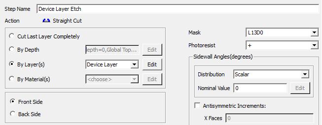
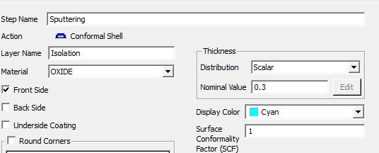
169 Step No: 2 Step No: 3 Step No: 4 155

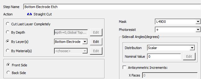
170 Step No: 5 Step No: 6 Step No: 7 156

171 Step No: 8 Step No: 9 Step No:

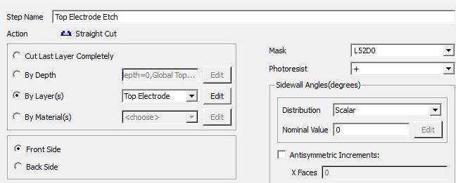
172 Step No: 11 Step No: 12 Step No:

173 A-3 List of material properties used in the analytical and FEM modeling - Si <100> Young s modulus E = GPa - PZT Young s modulus E = 89 GPa - Gold Young s modulus E = 57 GPa - Platinum Young s modulus E = 145 GPa - Transverse piezoelectric coefficient d 31 = 274e-12 m/v - Electromechanical coupling coefficient k 31 = Dielectric constant of the piezoelectric material under free conditions; ε ₃₃ = 1700 F/m 159


174 Appendix B B-1 Cross Tethers CoventorWare Process Editor Fabrication Process Step No: 0 Step No: 1 160

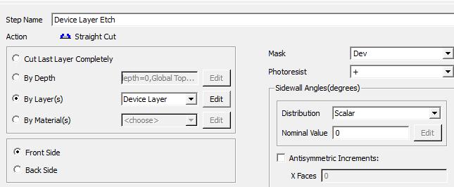
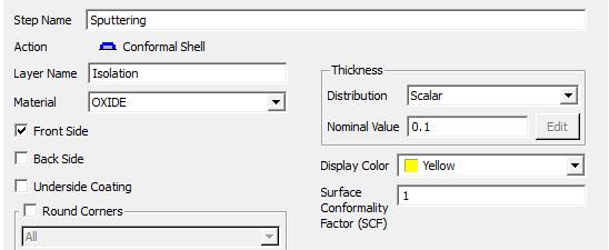
175 Step No: 2 Step No: 3 Step No: 4 161

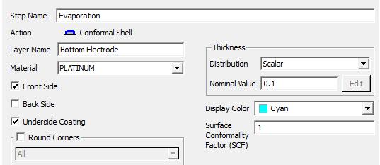
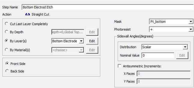
176 Step No: 5 Step No: 6 Step No: 7 162

177 Step No: 8 Step No: 9 Step No:

178 Step No: 11 Step No: 12 Step No:


179 B-2 Cross tethers configuration modal analysis results Table 26. Cross Tethers Configuration FEM resonant frequencies results Table 27. Cross Tethers generalized harmonic display results 165
180 Mode 1 ( Hz) Mode 2 ( Hz) Mode 3 ( Hz) Mode 4 ( Hz) Mode 5 ( Hz) Mode 6 ( Hz) Figure 58. Cross tethers resulting vibrating pattern and associated resonant frequencies for a load of 10 mpa 166
181 Mode 1 ( Hz) Mode 2 ( Hz) Mode 3 ( Hz) Mode 4 ( Hz) Mode 5 ( Hz) Mode 6 ( Hz) Figure 59. Cross Tethers Generalized Displacements plots 167


182 Appendix C C-1 Circular Membrane CoventorWare Process Editor Fabrication Process Step No: 0 Step No: 1 168

183 Step No: 2 Step No: 3 Step No: 4 169

184 Step No: 5 Step No: 6 Step No: 7 170


185 C-2 Circular Membrane FEM Modal and Mises Stress analysis results As mentioned in Section 4.5 the additional results presented in this appendix section provide a deeper insight into circular membrane insensitivity. As can be seen in Table 29 that depict modal analysis results, membrane (with overall thickness of 2. 6μm) does not respond at all even for photoacoustic pressure load of 5 Pa. Responses associated with Mode 3, Mode 4, and Mode 6 is clearly zero while response associated with remaining modes are well below measurable levels. The same observations can be seen from Figure 57 and Figure 58. Table 28. Circular membrane FEM natural resonant frequencies results Table 29. Circular membrane generalized harmonic display results 171
 Figure 60.")
186 Mode 1 ( Hz) Mode 2 ( Hz) Mode 3 ( Hz) Mode 4 ( Hz) Mode 5 ( Hz) Mode 6 ( Hz) Figure 60. Circular membrane resulting vibrating pattern and resonant frequencies for a load of 5 Pa 172
187 Mode 1 ( Hz) Mode 2 ( Hz) Mode 3 ( Hz) Mode 4 ( Hz) Mode 5 ( Hz) Mode 6 ( Hz) Figure 61. Circular Membrane Generalized Displacements plots 173
 between the membrane and the surrounding silicon frame is only 0.83nm.")
188 Figure 62. FEM model result of the deflection of a clamped circular membrane for 5 Pa photoacoustic load. As can be seen in Figure 62 the maximum deflection of 5.1μm occurs at the center of membrane. The figure also shows that the deflection at fixed boundary (red color) between the membrane and the surrounding silicon frame is only 0.83nm. This deflection in critical stress area is so small that will not create any effective stress and charge generation at all as explained in Section 4.5. Furthermore, Figure 63 below, which is FEM Mises stress representation, clearly indicates that there is no radial and tangential stress generation as result of uniformly distributed pressure load. 174
189 Figure 63. Circular Membrane FEM Mises stress distribution for 5 Pa photoacoustic pressure load 175


190 Appendix D D-1 Square Membrane CoventorWare Process Editor Fabrication Process Step No: 0 Step No: 1 176

191 Step No: 2 Step No: 3 Step No: 4 177

192 Step No: 5 Step No: 6 Step No: 7 178

193 Step No: 8 Step No: 9 Step No:

194 D-2 Square Membrane FEM results for 0.52 µm x 0.52 µm PZT transducers Figure 64. FEM 3D meshed model of the square membrane (Extruded bricks, element order parabolic, element size in planar direction 200, element size in extrude direction 5) 180

195 Table 30. Generated voltages for the square membrane sensing configuration involving PZT transducers of 0.3 µm x 0.3 µm and 0.52 µm x 0.52 µm Figure 65. Square membrane deflection for 10mPa uniformly distributed pressure load 181

196 Figure 66. Mises stress distribution of a square membrane configuration involving 0.52 µm x 0.52 µm PZT transducers 182
Outline. 4 Mechanical Sensors Introduction General Mechanical properties Piezoresistivity Piezoresistive Sensors Capacitive sensors Applications
 Sensor devices Outline 4 Mechanical Sensors Introduction General Mechanical properties Piezoresistivity Piezoresistive Sensors Capacitive sensors Applications Introduction Two Major classes of mechanical
PIEZOELECTRIC TECHNOLOGY PRIMER
 PIEZOELECTRIC TECHNOLOGY PRIMER James R. Phillips Sr. Member of Technical Staff CTS Wireless Components 4800 Alameda Blvd. N.E. Albuquerque, New Mexico 87113 Piezoelectricity The piezoelectric effect is
Foundations of MEMS. Chang Liu. McCormick School of Engineering and Applied Science Northwestern University. International Edition Contributions by
 Foundations of MEMS Second Edition Chang Liu McCormick School of Engineering and Applied Science Northwestern University International Edition Contributions by Vaishali B. Mungurwadi B. V. Bhoomaraddi
Finite Element Analysis of Piezoelectric Cantilever
 Finite Element Analysis of Piezoelectric Cantilever Nitin N More Department of Mechanical Engineering K.L.E S College of Engineering and Technology, Belgaum, Karnataka, India. Abstract- Energy (or power)
SENSOR DEVICES MECHANICAL SENSORS
 SENSOR DEVICES MECHANICAL SENSORS OUTLINE 4 Mechanical Sensors Introduction General mechanical properties Piezoresistivity Piezoresistive sensors Capacitive sensors Applications INTRODUCTION MECHANICAL
Piezoelectric Resonators ME 2082
 Piezoelectric Resonators ME 2082 Introduction K T : relative dielectric constant of the material ε o : relative permittivity of free space (8.854*10-12 F/m) h: distance between electrodes (m - material
CHAPTER 4 DESIGN AND ANALYSIS OF CANTILEVER BEAM ELECTROSTATIC ACTUATORS
 61 CHAPTER 4 DESIGN AND ANALYSIS OF CANTILEVER BEAM ELECTROSTATIC ACTUATORS 4.1 INTRODUCTION The analysis of cantilever beams of small dimensions taking into the effect of fringing fields is studied and
INF5490 RF MEMS. LN03: Modeling, design and analysis. Spring 2008, Oddvar Søråsen Department of Informatics, UoO
 INF5490 RF MEMS LN03: Modeling, design and analysis Spring 2008, Oddvar Søråsen Department of Informatics, UoO 1 Today s lecture MEMS functional operation Transducer principles Sensor principles Methods
An Accurate Model for Pull-in Voltage of Circular Diaphragm Capacitive Micromachined Ultrasonic Transducers (CMUT)
") An Accurate Model for Pull-in Voltage of Circular Diaphragm Capacitive Micromachined Ultrasonic Transducers (CMUT) Mosaddequr Rahman, Sazzadur Chowdhury Department of Electrical and Computer Engineering
An Accurate Model for Pull-in Voltage of Circular Diaphragm Capacitive Micromachined Ultrasonic Transducers (CMUT) Mosaddequr Rahman, Sazzadur Chowdhury Department of Electrical and Computer Engineering
Microstructure cantilever beam for current measurement
 264 South African Journal of Science 105 July/August 2009 Research Articles Microstructure cantilever beam for current measurement HAB Mustafa and MTE Khan* Most microelectromechanical systems (MEMS) sensors
Slide 1. Temperatures Light (Optoelectronics) Magnetic Fields Strain Pressure Displacement and Rotation Acceleration Electronic Sensors
 Magnetic Fields Strain Pressure Displacement and Rotation Acceleration Electronic Sensors") Slide 1 Electronic Sensors Electronic sensors can be designed to detect a variety of quantitative aspects of a given physical system. Such quantities include: Temperatures Light (Optoelectronics) Magnetic
Slide 1 Electronic Sensors Electronic sensors can be designed to detect a variety of quantitative aspects of a given physical system. Such quantities include: Temperatures Light (Optoelectronics) Magnetic
Piezoresistive Sensors
 Piezoresistive Sensors Outline Piezoresistivity of metal and semiconductor Gauge factor Piezoresistors Metal, silicon and polysilicon Close view of the piezoresistivity of single crystal silicon Considerations
Thickness Optimization of a Piezoelectric Converter for Energy Harvesting
 Excerpt from the Proceedings of the COMSOL Conference 29 Milan Thickness Optimization of a Piezoelectric Converter for Energy Harvesting M. Guizzetti* 1, V. Ferrari 1, D. Marioli 1 and T. Zawada 2 1 Dept.
DESIGN AND SIMULATION OF UNDER WATER ACOUSTIC MEMS SENSOR
 DESIGN AND SIMULATION OF UNDER WATER ACOUSTIC MEMS SENSOR Smitha G Prabhu 1, Nagabhushana S *2 1 Dept. Of Electronics and communication, Center for Nano Materials and MEMS, 2 Dept. of Electronics and Communication,
Design And Analysis of Microcantilevers Type Sensor With Different Shape of Piezoresistive Patch
 Aakash Swami, Pulkit Agarwal 45 Design And Analysis of Microcantilevers Type Sensor With Different Shape of Piezoresistive Patch Aakash Swami and Pulkit Agarwal Student MNNIT Allahabad Email:aakashswami7@gmail.com
Active elastomer components based on dielectric elastomers
 Gummi Fasern Kunststoffe, 68, No. 6, 2015, pp. 412 415 Active elastomer components based on dielectric elastomers W. Kaal and S. Herold Fraunhofer Institute for Structural Durability and System Reliability
Effect of Strain Nodes and Electrode Configuration on Piezoelectric Energy Harvesting From Cantilevered Beams
 A. Erturk 1 Center for Intelligent Material Systems and Structures, Department of Engineering Science and Mechanics, Virginia Tech, Blacksburg, VA 24061 e-mail: erturk@vt.edu P. A. Tarazaga J. R. Farmer
ACCURATE MODELLING OF STRAIN DISCONTINUITIES IN BEAMS USING AN XFEM APPROACH
 VI International Conference on Adaptive Modeling and Simulation ADMOS 213 J. P. Moitinho de Almeida, P. Díez, C. Tiago and N. Parés (Eds) ACCURATE MODELLING OF STRAIN DISCONTINUITIES IN BEAMS USING AN
CHAPTER 5 FIXED GUIDED BEAM ANALYSIS
 77 CHAPTER 5 FIXED GUIDED BEAM ANALYSIS 5.1 INTRODUCTION Fixed guided clamped and cantilever beams have been designed and analyzed using ANSYS and their performance were calculated. Maximum deflection
Lecture 20. Measuring Pressure and Temperature (Chapter 9) Measuring Pressure Measuring Temperature MECH 373. Instrumentation and Measurements
 Measuring Pressure Measuring Temperature MECH 373. Instrumentation and Measurements") MECH 373 Instrumentation and Measurements Lecture 20 Measuring Pressure and Temperature (Chapter 9) Measuring Pressure Measuring Temperature 1 Measuring Acceleration and Vibration Accelerometers using
MECH 373 Instrumentation and Measurements Lecture 20 Measuring Pressure and Temperature (Chapter 9) Measuring Pressure Measuring Temperature 1 Measuring Acceleration and Vibration Accelerometers using
ANALYSIS AND NUMERICAL MODELLING OF CERAMIC PIEZOELECTRIC BEAM BEHAVIOR UNDER THE EFFECT OF EXTERNAL SOLICITATIONS
 Third International Conference on Energy, Materials, Applied Energetics and Pollution. ICEMAEP016, October 30-31, 016, Constantine,Algeria. ANALYSIS AND NUMERICAL MODELLING OF CERAMIC PIEZOELECTRIC BEAM
Institute for Electron Microscopy and Nanoanalysis Graz Centre for Electron Microscopy
 Institute for Electron Microscopy and Nanoanalysis Graz Centre for Electron Microscopy Micromechanics Ass.Prof. Priv.-Doz. DI Dr. Harald Plank a,b a Institute of Electron Microscopy and Nanoanalysis, Graz
Structural Dynamics Lecture Eleven: Dynamic Response of MDOF Systems: (Chapter 11) By: H. Ahmadian
 By: H. Ahmadian") Structural Dynamics Lecture Eleven: Dynamic Response of MDOF Systems: (Chapter 11) By: H. Ahmadian ahmadian@iust.ac.ir Dynamic Response of MDOF Systems: Mode-Superposition Method Mode-Superposition Method:
Structural Dynamics Lecture Eleven: Dynamic Response of MDOF Systems: (Chapter 11) By: H. Ahmadian ahmadian@iust.ac.ir Dynamic Response of MDOF Systems: Mode-Superposition Method Mode-Superposition Method:
Electromechanical Sensors and Actuators Fall Term
 Electromechanical Sensors and Actuators Dr. Qing-Ming Wang Professor of Mechanical Engineering and Materials Science University of Pittsburgh 2017 Fall Term Lecture 1 Introduction and Transducer Models
Biosensors and Instrumentation: Tutorial 2
 Biosensors and Instrumentation: Tutorial 2. One of the most straightforward methods of monitoring temperature is to use the thermal variation of a resistor... Suggest a possible problem with the use of
Solid State Physics (condensed matter): FERROELECTRICS
: FERROELECTRICS") Solid State Physics (condensed matter): FERROELECTRICS Prof. Igor Ostrovskii The University of Mississippi Department of Physics and Astronomy Oxford, UM: May, 2012 1 People: Solid State Physics Condensed
Solid State Physics (condensed matter): FERROELECTRICS Prof. Igor Ostrovskii The University of Mississippi Department of Physics and Astronomy Oxford, UM: May, 2012 1 People: Solid State Physics Condensed
Piezoelectric Actuator for Micro Robot Used in Nanosatellite
 Piezoelectric Actuator for Micro Robot Used in Nanosatellite R Bansevicius, S Navickaite, V Jurenas and A Bubulis PIEZOELECTRIC ACTUATOR FOR MICRO ROBOT USED IN NANOSATELLITE. R Bansevicius 1, S Navickaite,
EE 5344 Introduction to MEMS CHAPTER 6 Mechanical Sensors. 1. Position Displacement x, θ 2. Velocity, speed Kinematic
 I. Mechanical Measurands: 1. Classification of main types: EE 5344 Introduction MEMS CHAPTER 6 Mechanical Sensors 1. Position Displacement x, θ. Velocity, speed Kinematic dx dθ v =, = ω 3. Acceleration
Design and Simulation of a Novel MEMS Bidirectional Anemometer
 2013, TextRoad Publication ISSN 2090-4304 Journal of Basic and Applied Scientific Research www.textroad.com Design and Simulation of a Novel MEMS Bidirectional Anemometer Ali Pazoki Nezhad 1 and Mohamad
Principles of Active Vibration Control: Piezoelectric materials
 Principles of Active Vibration Control: Piezoelectric materials Introduction: Piezoelectric materials are materials that produce a voltage when stress is applied. Since, this effect also applies in the
SENSORS and TRANSDUCERS
 SENSORS and TRANSDUCERS Tadeusz Stepinski, Signaler och system The Mechanical Energy Domain Physics Surface acoustic waves Silicon microresonators Variable resistance sensors Piezoelectric sensors Capacitive
3. BEAMS: STRAIN, STRESS, DEFLECTIONS
 3. BEAMS: STRAIN, STRESS, DEFLECTIONS The beam, or flexural member, is frequently encountered in structures and machines, and its elementary stress analysis constitutes one of the more interesting facets
INTRODUCTION TO PIEZO TRANSDUCERS
 PIEZO SYSTEMS, INC. 65 Tower Office Park Woburn, MA 01801 USA Tel: 781 933 4850 Fax: 781 933 4743 email: sales@piezo.com Find Search for a product or category HOME PRODUCTS CUSTOM OEM CATALOG TECHNICAL
Piezoelectric Multilayer Beam Bending Actuators
 R.G. Bailas Piezoelectric Multilayer Beam Bending Actuators Static and Dynamic Behavior and Aspects of Sensor Integration With 143 Figures and 17 Tables Sprin ger List of Symbols XV Part I Focus of the
Midterm 2 PROBLEM POINTS MAX
 Midterm 2 PROBLEM POINTS MAX 1 30 2 24 3 15 4 45 5 36 1 Personally, I liked the University; they gave us money and facilities, we didn't have to produce anything. You've never been out of college. You
How Does a Microcantilever Work?
 How Does a Cantilever Work? Participant Guide Description and Estimated Time to Complete The microcantilever is a widely used component in microsystems devices or microelectromechanical systems (MEMS).
Piezo materials. Actuators Sensors Generators Transducers. Piezoelectric materials may be used to produce e.g.: Piezo materials Ver1404
 Noliac Group develops and manufactures piezoelectric materials based on modified lead zirconate titanate (PZT) of high quality and tailored for custom specifications. Piezoelectric materials may be used
Integrating MEMS Electro-Static Driven Micro-Probe and Laser Doppler Vibrometer for Non-Contact Vibration Mode SPM System Design
 Tamkang Journal of Science and Engineering, Vol. 12, No. 4, pp. 399 407 (2009) 399 Integrating MEMS Electro-Static Driven Micro-Probe and Laser Doppler Vibrometer for Non-Contact Vibration Mode SPM System
MODELING OF T-SHAPED MICROCANTILEVER RESONATORS. Margarita Narducci, Eduard Figueras, Isabel Gràcia, Luis Fonseca, Joaquin Santander, Carles Cané
 Stresa, Italy, 5-7 April 007 MODELING OF T-SHAPED MICROCANTILEVER RESONATORS Margarita Narducci, Eduard Figueras, Isabel Gràcia, Luis Fonseca, Joaquin Santander, Carles Centro Nacional de Microelectrónica
Chapter 5 Structural Elements: The truss & beam elements
 Institute of Structural Engineering Page 1 Chapter 5 Structural Elements: The truss & beam elements Institute of Structural Engineering Page 2 Chapter Goals Learn how to formulate the Finite Element Equations
Table of Contents. Preface... 13
 Table of Contents Preface... 13 Chapter 1. Vibrations of Continuous Elastic Solid Media... 17 1.1. Objective of the chapter... 17 1.2. Equations of motion and boundary conditions of continuous media...
SIMULATION AND OPTIMIZATION OF MEMS PIEZOELECTRIC ENERGY HARVESTER WITH A NON-TRADITIONAL GEOMETRY
 SIMULATION AND OPTIMIZATION OF MEMS PIEZOELECTRIC ENERGY HARVESTER WITH A NON-TRADITIONAL GEOMETRY S. Sunithamani 1, P. Lakshmi 1, E. Eba Flora 1 1 Department of EEE, College of Engineering, Anna University,
Design and Simulation of Comb Drive Capacitive Accelerometer by Using MEMS Intellisuite Design Tool
 Design and Simulation of Comb Drive Capacitive Accelerometer by Using MEMS Intellisuite Design Tool Gireesh K C 1, Harisha M 2, Karthick Raj M 3, Karthikkumar M 4, Thenmoli M 5 UG Students, Department
NUMERICAL EVALUATION OF A TEFLON BASED PIEZOELECTRIC SENSOR EFFECTIVITY FOR THE MONITORING OF EARLY AGE COCRETE STRENGTHING
 NUMERICAL EVALUATION OF A TEFLON BASED PIEZOELECTRIC SENSOR EFFECTIVITY FOR THE MONITORING OF EARLY AGE COCRETE STRENGTHING Evangelos V. Liarakos Postdoctoral researcher School of Architecture, Technical
Lecture 19. Measurement of Solid-Mechanical Quantities (Chapter 8) Measuring Strain Measuring Displacement Measuring Linear Velocity
 Measuring Strain Measuring Displacement Measuring Linear Velocity") MECH 373 Instrumentation and Measurements Lecture 19 Measurement of Solid-Mechanical Quantities (Chapter 8) Measuring Strain Measuring Displacement Measuring Linear Velocity Measuring Accepleration and
MECH 373 Instrumentation and Measurements Lecture 19 Measurement of Solid-Mechanical Quantities (Chapter 8) Measuring Strain Measuring Displacement Measuring Linear Velocity Measuring Accepleration and
Modeling, Simulation and Optimization of the Mechanical Response of Micromechanical Silicon Cantilever: Application to Piezoresistive Force Sensor
 Available online at www.sciencedirect.com ScienceDirect Physics Procedia 55 (2014 ) 348 355 Eight International Conference on Material Sciences (CSM8-ISM5) Modeling, Simulation and Optimization of the
EE C245 ME C218 Introduction to MEMS Design
 EE C245 ME C218 Introduction to MEMS Design Fall 2007 Prof. Clark T.-C. Nguyen Dept. of Electrical Engineering & Computer Sciences University of California at Berkeley Berkeley, CA 94720 Lecture 16: Energy
[8] Bending and Shear Loading of Beams
![[8] Bending and Shear Loading of Beams](/thumbs/92/110949676.jpg "[8] Bending and Shear Loading of Beams") [8] Bending and Shear Loading of Beams Page 1 of 28 [8] Bending and Shear Loading of Beams [8.1] Bending of Beams (will not be covered in class) [8.2] Bending Strain and Stress [8.3] Shear in Straight
[8] Bending and Shear Loading of Beams Page 1 of 28 [8] Bending and Shear Loading of Beams [8.1] Bending of Beams (will not be covered in class) [8.2] Bending Strain and Stress [8.3] Shear in Straight
Natural vibration frequency of classic MEMS structures
 Natural vibration frequency of classic MEMS structures Zacarias E. Fabrim PGCIMAT, UFRGS, Porto Alegre, RS, Brazil Wang Chong, Manoel Martín Pérez Reimbold DeTec, UNIJUI, Ijuí, RS, Brazil Abstract This
Piezoelectric Control of Multi-functional Composite Shells Subjected to an Electromagnetic Field
 Piezoelectric Control of Multi-functional Composite Shells Subjected to an Electromagnetic Field *Sang-Yun Park 1) and Ohseop Song 2) 1), 2) Department of Mechanical Engineering, Chungnam National University,
Design of a MEMS Capacitive Comb-drive Accelerometer
 Design of a MEMS Capacitive Comb-drive Accelerometer Tolga Kaya* 1, Behrouz Shiari 2, Kevin Petsch 1 and David Yates 2 1 Central Michigan University, 2 University of Michigan * kaya2t@cmich.edu Abstract:
Bending Load & Calibration Module
 Bending Load & Calibration Module Objectives After completing this module, students shall be able to: 1) Conduct laboratory work to validate beam bending stress equations. 2) Develop an understanding of
Physical Phenomena Used in Sensors
 Physical Phenomena Used in Sensors Tiantian Xie Auburn University Bogdan M. Wilamowski Auburn University. Introduction... -. Piezoresistive Effect... -.3 Thermoelectric Effect...-5.4 Piezoelectric Effect...-5.5
ENG2000 Chapter 7 Beams. ENG2000: R.I. Hornsey Beam: 1
 ENG2000 Chapter 7 Beams ENG2000: R.I. Hornsey Beam: 1 Overview In this chapter, we consider the stresses and moments present in loaded beams shear stress and bending moment diagrams We will also look at
7. CONCLUSIONS & SCOPE
 7. CONCLUSIONS & SCOPE ENERGY harvesting is a critical technology for the expansion of self-governing, self-powered electronic devices. As the energy requirements of low-power electronics reduction, the
Transduction Based on Changes in the Energy Stored in an Electrical Field
 Lecture 7-1 Transduction Based on Changes in the Energy Stored in an Electrical Field - Electrostriction The electrostrictive effect is a quadratic dependence of strain or stress on the polarization P
VIBRATION CONTROL OF RECTANGULAR CROSS-PLY FRP PLATES USING PZT MATERIALS
 Journal of Engineering Science and Technology Vol. 12, No. 12 (217) 3398-3411 School of Engineering, Taylor s University VIBRATION CONTROL OF RECTANGULAR CROSS-PLY FRP PLATES USING PZT MATERIALS DILEEP
Sensors & Transducers 2016 by IFSA Publishing, S. L.
 Sensors & Transducers, Vol. 96, Issue, January 206, pp. 52-56 Sensors & Transducers 206 by IFSA Publishing, S. L. http://www.sensorsportal.com Collapse Mode Characteristics of Parallel Plate Ultrasonic
Published by: PIONEER RESEARCH & DEVELOPMENT GROUP(
 MEMS based Piezo resistive Pressure Sensor Swathi Krishnamurthy 1, K.V Meena 2, E & C Engg. Dept., The Oxford College of Engineering, Karnataka. Bangalore 560009 Abstract The paper describes the performance
Lecture 15 Strain and stress in beams
 Spring, 2019 ME 323 Mechanics of Materials Lecture 15 Strain and stress in beams Reading assignment: 6.1 6.2 News: Instructor: Prof. Marcial Gonzalez Last modified: 1/6/19 9:42:38 PM Beam theory (@ ME
Symmetric Bending of Beams
 Symmetric Bending of Beams beam is any long structural member on which loads act perpendicular to the longitudinal axis. Learning objectives Understand the theory, its limitations and its applications
Vibro-Impact Dynamics of a Piezoelectric Energy Harvester
 Proceedings of the IMAC-XXVIII February 1 4, 1, Jacksonville, Florida USA 1 Society for Experimental Mechanics Inc. Vibro-Impact Dynamics of a Piezoelectric Energy Harvester K.H. Mak *, S. McWilliam, A.A.
The New Boundary Condition Effect on The Free Vibration Analysis of Micro-beams Based on The Modified Couple Stress Theory
 International Research Journal of Applied and Basic Sciences 2015 Available online at www.irjabs.com ISSN 2251-838X / Vol, 9 (3): 274-279 Science Explorer Publications The New Boundary Condition Effect
202 Index. failure, 26 field equation, 122 force, 1
 Index acceleration, 12, 161 admissible function, 155 admissible stress, 32 Airy's stress function, 122, 124 d'alembert's principle, 165, 167, 177 amplitude, 171 analogy, 76 anisotropic material, 20 aperiodic
Design And Analysis of Microcantilevers With Various Shapes Using COMSOL Multiphysics Software
 Design And Analysis of Microcantilevers With Various Shapes Using COMSOL Multiphysics Software V. Mounika Reddy 1, G.V.Sunil Kumar 2 1,2 Department of Electronics and Instrumentation Engineering, Sree
Modeling of Photoinduced Deformation in Silicon Microcantilevers
 Sensors 007, 7, 73-79 sensors ISSN 44-80 007 by DPI www.mdpi.org/sensors Full Paper odeling of Photoinduced Deformation in Silicon icrocantilevers Yu-Lin Guo, Jia Zhou *, Yiping uang and in ang Bao ASIC
UNIVERSITY OF CAMBRIDGE INTERNATIONAL EXAMINATIONS General Certificate of Education Advanced Level
 UNIVERSITY OF CAMBRIDGE INTERNATIONAL EXAMINATIONS General Certificate of Education Advanced Level *2900417311* PHYSICS 9702/42 Paper 4 A2 Structured Questions October/November 2010 1 hour 45 minutes Candidates
Shape Effect of Piezoelectric Energy Harvester on Vibration Power Generation
 Journal of Power and Energy Engineering, 014,, 117-14 Published Online September 014 in SciRes. http://www.scirp.org/journal/jpee http://dx.doi.org/10.436/jpee.014.9017 Shape Effect of Piezoelectric Energy
COPYRIGHTED MATERIAL. Index
 Index A Admissible function, 163 Amplification factor, 36 Amplitude, 1, 22 Amplitude-modulated carrier, 630 Amplitude ratio, 36 Antinodes, 612 Approximate analytical methods, 647 Assumed modes method,
Soft Bodies. Good approximation for hard ones. approximation breaks when objects break, or deform. Generalization: soft (deformable) bodies
 bodies") Soft-Body Physics Soft Bodies Realistic objects are not purely rigid. Good approximation for hard ones. approximation breaks when objects break, or deform. Generalization: soft (deformable) bodies Deformed
Soft-Body Physics Soft Bodies Realistic objects are not purely rigid. Good approximation for hard ones. approximation breaks when objects break, or deform. Generalization: soft (deformable) bodies Deformed
The Analysis of Aluminium Cantilever Beam with Piezoelectric Material by changing Position of piezo patch over Length of Beam
 The Analysis of Aluminium Cantilever Beam with Piezoelectric Material by changing Position of piezo patch over Length of Beam Mr. Lalit R. Shendre 1, Prof. Bhamare V.G. 2 1PG Student, Department of Mechanical
Finite Element Analysis Prof. Dr. B. N. Rao Department of Civil Engineering Indian Institute of Technology, Madras. Module - 01 Lecture - 11
 Finite Element Analysis Prof. Dr. B. N. Rao Department of Civil Engineering Indian Institute of Technology, Madras Module - 01 Lecture - 11 Last class, what we did is, we looked at a method called superposition
MEMS Tuning-Fork Gyroscope Mid-Term Report Amanda Bristow Travis Barton Stephen Nary
 MEMS Tuning-Fork Gyroscope Mid-Term Report Amanda Bristow Travis Barton Stephen Nary Abstract MEMS based gyroscopes have gained in popularity for use as rotation rate sensors in commercial products like
7.4 The Elementary Beam Theory
 7.4 The Elementary Beam Theory In this section, problems involving long and slender beams are addressed. s with pressure vessels, the geometry of the beam, and the specific type of loading which will be
Optimal Location of an Active Segment of Magnetorheological Fluid Layer in a Sandwich Plate
 Acta Montanistica Slovaca Ročník 16 (2011), číslo 1, 95-100 Optimal Location of an Active Segment of Magnetorheological Fluid Layer in a Sandwich Plate Jacek Snamina 1 Abstract: In the present study a
Physics Important Terms and their Definitions
 Physics Important Terms and their S.No Word Meaning 1 Acceleration The rate of change of velocity of an object with respect to time 2 Angular Momentum A measure of the momentum of a body in rotational
Mechanics of Inflatable Fabric Beams
 Copyright c 2008 ICCES ICCES, vol.5, no.2, pp.93-98 Mechanics of Inflatable Fabric Beams C. Wielgosz 1,J.C.Thomas 1,A.LeVan 1 Summary In this paper we present a summary of the behaviour of inflatable fabric
Structural Dynamics A Graduate Course in Aerospace Engineering
 Structural Dynamics A Graduate Course in Aerospace Engineering By: H. Ahmadian ahmadian@iust.ac.ir The Science and Art of Structural Dynamics What do all the followings have in common? > A sport-utility
Chapter 6. Fiber Optic Thermometer. Ho Suk Ryou
 Chapter 6. Fiber Optic Thermometer Ho Suk Ryou Properties of Optical Fiber Optical Fiber Composed of rod core surrounded by sheath Core: conducts electromagnetic wave Sheath: contains wave within the core
Finite Element Analysis and Experiment on a Piezoelectric Harvester with Multiple Cantilevers
 doi: 10.14355/ijep.2015.04.003 Finite Element Analysis and Experiment on a Piezoelectric Harvester with Multiple Cantilevers Hongbing WANG *1, Chunhua SUN 2, Zhirong LI 3, Yiping ZhANG 4 Department of
Active Integral Vibration Control of Elastic Bodies
 Applied and Computational Mechanics 2 (2008) 379 388 Active Integral Vibration Control of Elastic Bodies M. Smrž a,m.valášek a, a Faculty of Mechanical Engineering, CTU in Prague, Karlovo nam. 13, 121
DESIGN AND APPLICATION
 III. 3.1 INTRODUCTION. From the foregoing sections on contact theory and material properties we can make a list of what properties an ideal contact material would possess. (1) High electrical conductivity
SENSORS AND TRANSDUCERS
 Electrical Measurements International Program Department of Electrical Engineering UNIVERSITAS INDONESIA ANDRITTO ABDUL GHAFFAR ANDHIKA ADIEL INSANI Lecturer : Ir. Chairul Hudaya, ST, M.Eng., Ph.D., IPM
Chapter 5 Elastic Strain, Deflection, and Stability 1. Elastic Stress-Strain Relationship
 Chapter 5 Elastic Strain, Deflection, and Stability Elastic Stress-Strain Relationship A stress in the x-direction causes a strain in the x-direction by σ x also causes a strain in the y-direction & z-direction
EE C245 ME C218 Introduction to MEMS Design Fall 2007
 EE C245 ME C218 Introduction to MEMS Design Fall 2007 Prof. Clark T.-C. Nguyen Dept. of Electrical Engineering & Computer Sciences University of California at Berkeley Berkeley, CA 94720 Lecture 17: Energy
Innovative MEMS Voltage-to-Frequency Converter using Cascaded Transducers
 International Journal of Engineering and Technology Volume 2 No. 9, September, 2012 Innovative MEMS Voltage-to-Frequency Converter using Cascaded Transducers Amir J. Majid Ajman University of Science &
EE C247B / ME C218 INTRODUCTION TO MEMS DESIGN SPRING 2014 C. Nguyen PROBLEM SET #4
 Issued: Wednesday, Mar. 5, 2014 PROBLEM SET #4 Due (at 9 a.m.): Tuesday Mar. 18, 2014, in the EE C247B HW box near 125 Cory. 1. Suppose you would like to fabricate the suspended cross beam structure below
Problem Solver Skill 5. Defines multiple or complex problems and brainstorms a variety of solutions
 Motion and Forces Broad Concept: Newton s laws of motion and gravitation describe and predict the motion of most objects. LS 1.1 Compare and contrast vector quantities (such as, displacement, velocity,
1 Force Sensing. Lecture Notes. 1.1 Load Cell. 1.2 Stress and Strain
 Lecture Notes 1 Force Sensing 1.1 Load Cell A Load Cell is a structure which supports the load and deflects a known amount in response to applied forces and torques. The deflections are measured to characterize
St Olave s Grammar School. AS Physics Mock Revision Checklist
 St Olave s Grammar School Mock Practical skills.. a Can you design experiments, including ones to solve problems set in a practical context?.. b Can you identify the variables that must be controlled in
ME 515 Mechatronics. Overview of Computer based Control System
 ME 515 Mechatronics Introduction to Sensors I Asanga Ratnaweera Department of Faculty of Engineering University of Peradeniya Tel: 081239 (3627) Email: asangar@pdn.ac.lk Overview of Computer based Control
10 Measurement of Acceleration, Vibration and Shock Transducers
 Chapter 10: Acceleration, Vibration and Shock Measurement Dr. Lufti Al-Sharif (Revision 1.0, 25/5/2008) 1. Introduction This chapter examines the measurement of acceleration, vibration and shock. It starts
Strain, Force, and Pressure
 10-1 10-1 Strain, Force, and Pressure Force is that which results in acceleration (when forces don t cancel). Strain is the change in shape of an object...... usually due to some force. (Force is usually
Modeling and simulation of multiport RF switch
 Journal of Physics: Conference Series Modeling and simulation of multiport RF switch To cite this article: J Vijay et al 006 J. Phys.: Conf. Ser. 4 715 View the article online for updates and enhancements.
I. MEASUREMENT OF TEMPERATURE
 I. MEASUREMENT OF TEMPERATURE Most frequent measurement and control Direct contact: thermometer, Indirect contact: pyrometer (detect generated heat or sensing optical properties) 1. Definition of temperature
Transduction Based on Changes in the Energy Stored in an Electrical Field. Lecture 6-5. Department of Mechanical Engineering
 Transduction Based on Changes in the Energy Stored in an Electrical Field Lecture 6-5 Transducers with cylindrical Geometry For a cylinder of radius r centered inside a shell with with an inner radius
HEALTH MONITORING OF PLATE STRUCTURE USING PIEZO ELECTRIC PATCHES AND CURVATURE MODE SHAPE
 ISSN (Online) : 2319-8753 ISSN (Print) : 2347-6710 International Journal of Innovative Research in Science, Engineering and Technology An ISO 3297: 2007 Certified Organization, Volume 2, Special Issue
Simulation based Analysis of Capacitive Pressure Sensor with COMSOL Multiphysics
 Simulation based Analysis of Capacitive Pressure Sensor with COMSOL Multiphysics Nisheka Anadkat MTech- VLSI Design, Hindustan University, Chennai, India Dr. M J S Rangachar Dean Electrical Sciences, Hindustan
440. Simulation and implementation of a piezoelectric sensor for harmonic in-situ strain monitoring
 440. Simulation and implementation of a piezoelectric sensor for harmonic in-situ strain monitoring 0. Incandela a, L. Goujon b, C. Barthod c University of Savoie, BP 80439 Annecy-le-Vieux CEDEX, France
Members Subjected to Torsional Loads
 Members Subjected to Torsional Loads Torsion of circular shafts Definition of Torsion: Consider a shaft rigidly clamped at one end and twisted at the other end by a torque T = F.d applied in a plane perpendicular