CHARACTERIZATION OF THE OXIDE-SEMICONDUCTOR INTERFACE IN 4H-SIC/SIO 2 STRUCTURES USING TEM
|
|
|
- Jemima Foster
- 5 years ago
- Views:
Transcription
 University of Maryland, College Park Thursday, August 14, 2014 *Supported by ARL under contract no.")
1 CHARACTERIZATION OF THE OXIDE-SEMICONDUCTOR INTERFACE IN 4H-SIC/SIO 2 STRUCTURES USING TEM AND XPS Joshua Taillon, 1 Karen Gaskell 2, Gang Liu, 3 Leonard Feldman, 3 Sarit Dahr, 4 Tsvetanka Zheleva, 5 Aivars Lelis, 5 and Lourdes Salamanca-Riba 1 9 th Annual SiC MOS Workshop ( SiC Device Review ) University of Maryland, College Park Thursday, August 14, 2014 *Supported by ARL under contract no. W911NF and W911NF Materials Science and Engineering, University of Maryland College Park 2 Chemistry and Biochemistry, University of Maryland College Park 3 Institute for Advanced Materials, Rutgers University 4 Department of Physics, Auburn University 5 U.S. Army Research Laboratory
2 Motivation and background 1 J. Taillon, L. Salamanca-Riba, et al., J. Appl. Phys. 113, (2013). 4 P. Jamet, et al., J. Appl. Phys., 90(10), 5058 (2001). 2 H. Watanabe, et al., Appl. Phys. Lett., 99(2), (2011). 5 X. Zhu, et al., Appl. Phys. Lett., 97(7), (2010). 3 P. Tanner, et al., J. Electron. Mater., 28(2), 109 (1999). 2
3 Central questions How do the structure and chemistry of the 4H-SiC/SiO 2 interface change under NO anneal? What do these changes tell us about the effects of the passivation process? 3
4 Outline Depth profiles and XPS Development and refinement of SiO 2 spin-etch technique Initial results from XPS depth profiles TEM-EELS on miscut samples Analysis of oxidized and NO annealed samples with various crystallographic orientations Future areas of inquiry TEM investigation of interfacial roughness Further XPS depth profiles, valence band modeling, etc. 4
5 SPIN-ETCH DEVELOPMENT FOR DEPTH PROFILES 5
6 Motivation for XPS spin-etch depth profiles By etching very close to the interface and performing angle-resolved XPS (ARXPS), we can learn about the differences caused by an NO post-oxidation anneal in a depth-sensitive manner Most etching/profiling techniques however, cause extreme modifications of the surface being investigated Sputtering not an option due to induced damage and preferential oxygen removal Dip etching difficult to control, and leaves significant residue How to faithfully profile the interfacial region? Need a technique that will not significantly modify interface or cause damage to underlying structure 6
7 Spin-etch Profiling Developed by Grunthaner, Grunthaner, and Vasquez for use on Si/SiO 2 interfaces in the 1970s 1,2 Further refined by Fenner et al. in the 1980s 3 Dropwise etching of SiO 2 proven to be a highly controllable technique, with very little contamination of surface compared to other methods Order of magnitude improvement in surface residue, as measured by XPS 3 (reported in monolayers) 1 F. J. Grunthaner, P. J. Grunthaner, R. P. Vasquez, B. F. Lewis, J. Maserjian and A. Madhukar, J. Vac. Sci. Technol., 16(5), 1443 (1979) 2 R. P. Vasquez and F. J. Grunthaner, J. Appl. Phys., 52(5), 3509 (1981). 3 D. B. Fenner, D. K. Biegelsen and R. D. Bringans, J. Appl. Phys., 66(1), 419 (1989). 7
 spinning at 3000 rpm on vacuum chuck Etchant solution is 10:1:1")


8 Etching experimental setup Small samples (1 x 0.5 cm) spinning at 3000 rpm on vacuum chuck Etchant solution is 10:1:1 ratio of EtOH:H 2 O:49.5% HF Rinse sample with alcohol and H 2 O before etching Manually pipette 25 μl drops in groups of 5 drops (each group is 1 step ) Dry sample using N 2 blow gun after each step Controls explored: Number of steps Oxide type (wet or dry SiO 2 on Si) Time etchant is left before drying Time between etch steps 8
9 UMD process refinement Refine techniques on similarly-sized SiO 2 /Si samples 1) Measure SiO 2 thickness profile using ellipsometry 2) Etch, changing some parameter to control 3) Remeasure SiO 2 thickness profile, taking etched amount as data point 9
10 Results control via number of etch steps Long exposure (~15 seconds between etch steps) Wet thermal oxide 0.8 nm removed per step 10
11 Results control via number of etch steps Short exposure (~2 seconds between steps) Wet thermal oxide 0.5 nm removed per step Short exposure (~2 seconds between steps) Dry thermal oxide 0.4 nm removed per step 11
12 Results control via etching time Controlled amount of time left on spinner after 9 short etch steps Dry thermal oxide 0.2 nm removed per second remaining on spinner Indicates additional etching, without introduction of more etchant; vapor phase etching means process timing is important 12
13 Results control via etching time Controlled duration of each step by varying time between each step from 2 to 15 seconds; 9 steps Dry thermal oxide 0.2 nm removed per second of step time Again, indicates that timing of process is critical, likely due to vapor effects 13
14 Uniformity of etch Spin etch process retains original oxide profile, indicating uniform etching Plots below show ellipsometry measurements of oxide thickness across SiC samples after 2 etch steps, retaining oxide profile 14
15 Process limitations Spin-etch is extremely effective at removing material from 1 monolayer up to about 10 nm Beyond this, unintended edge effects, accelerated etching, and cumulative error make the method unreliable It is expected that a dip etch (for large-scale removal) followed by spinetch would retain the desirous characteristics while being more efficient Trying to remove too much SiO 2 at once caused unintended over-etching of SiC samples for XPS analysis 15
16 INITIAL XPS RESULTS 16
17 Samples investigated 4 SiC/SiO 2 samples were provided by Rutgers All are n-type with cm -3 doping Two samples were just oxidized (labeled O1 and O2) Two samples received 2hr NO post-oxidation anneal (labeled N1 and N2) Starting oxide thicknesses were ~55nm First test was to see if there was any perceptible effect of our spin-etch process in the XPS Two of the samples were etched very slightly (about 2nm removed) Two were cleaned (EtOH rinse) and analyzed as received 17
18 Etch effects XPS Survey Spectra SiC N1 As-received SiC N2 After 2 etches SiC O1 As-received SiC O2 After 2 etches No immediately observable effect of spin-etch on XPS survey scans
19 CPS CPS Si 2p Si 2p 08/14/ J. Taillon/L. Salamanca-Riba Etch effects Si 2p signal s1_sio2etch.vms : Si 2p/5 s1_70_sio2etchl.vms : Si 2p/5 x 10 2 x Name Si 2p Si 2p Pos. FWHM L.Sh GL(30) GL(30) Area %Area Name Si 2p Si 2p Pos. FWHM L.Sh GL(30) GL(30) Area %Area Binding Energy (ev) Binding Energy (ev) Normal (90) degrees 20 degrees Two distinct angle measurements from same sample (etched with 2 steps) Si 2p signal in thick SiO 2 (that was etched with two steps) looks exactly as expected for normal bulk SiO 2, indicating that the spin-etch does not chemically modify the Si signal 19
20 Accidentally stripped all oxide 08/14/ J. Taillon/L. Salamanca-Riba SiC sample oxide profiles (ellipsometry) Areas of analysis for XPS 20
 angle 40º angle 20º angle Sample O1 completely")
21 XPS Results Si 2p Fit Si 2p with spin-orbit split components Constrained fit by known physical phenomena to reduce spurious peak fits, i.e, I 2p1/2 :I 2p3/2 = 1:2 3 components found: Substrate, oxide, and substrate surface/interface Normal (90 ) angle 40º angle 20º angle Sample O1 completely etched oxidized SiC sample 21
22 XPS Results Si 2p 3 / 2 Looking at the peak position (binding energy) for each sample, we can see something interesting: Thin oxide layers Sample Substrate Oxide(I o (I ) s ) Oxide(I o ) Substrate surface (I s ) O1 normal We can determine these samples were completely etched, and have reformed a native oxide that is at a lower binding energy O1 40º O1 20º N1 normal N1 40º N1 20º O2 normal Thicker oxide layers O2 40º These samples are at the normal SiO 2 binding energy, so some of the true oxide remains O2 20º N2 normal N2 40º N2 20º

23 XPS Si 2p 2p signals for Si in samples with thicker oxide do not show any evidence of suboxide or native oxide states Also no apparent influence of N in the Si 2p, but we might not expect to see it anyway due to the low concentration Normal angle 40º angle 20º angle O2 N2 23

24 XPS N 1s N1 N2 Normal angle 40º angle 20º angle 4 components found in constrained fit Primary peak is consistent with silicon nitride-like bonding Other peaks likely to be successively more oxygen bonding and/or carbon bonding N content decreases when thick oxide is present, and is still present after all original oxide is etched off N is localized in SiC near interface (like the recent paper from Rutgers 1 ) 1 Y. Xu, L. C. Feldman, et al., J. Appl. Phys., 115(3), (2014). 24
25 XPS N 1s Thin oxide layers Thicker oxide layers Elemental composition (peak area integration) Measurement C 1s % N 1s % O 1s % Si 2p % N1 - normal N1 40º N1 20º N2 normal N2 40º N2 20º N content decreases when thick oxide is present, and is still present after all original oxide is etched off N is localized in SiC near interface (like the recent paper from Rutgers 1 ) 1 Y. Xu, L. C. Feldman, et al., J. Appl. Phys., 115(3), (2014). 25
, but this needs more")
26 XPS C 1s O1 N1 Normal angle 40º angle 20º angle Appears there is more C bonded to higher electronegativity atoms than we would expect from just contamination Possible C-O bonding at the interface Appears that NO anneal might reduce C-O peak (and perhaps C-O defect), but this needs more investigation 26
27 XPS valence band Valence band is related to density of states Lots of information, but difficult to interpret and will need modeling Possible small differences (to be analyzed using principle component analysis) Future collaboration with N. Goldsman s group to investigate further O1 N1 Normal angle 40º angle 20º angle 27
28 Accidentally stripped all oxide 08/14/ J. Taillon/L. Salamanca-Riba SiC sample oxide profiles (ellipsometry) Areas of analysis for XPS 28
29 ln(1+ I o N s s / I s N o o ) XPS oxide thickness compared to ellipsometry ln(1+ I o N s s / I s N o o ) = d/( o cos slope = d/ Linear Fit of 1 Linear Fit of 2 Linear Fit of 3 Linear Fit of 4 Slope of line from different angle measurements is related to thickness and mean free path of electrons cos Slope=d/λ SiO2 XPS d O1 = 0.38 nm N1 = 0.25 nm O2 = 6.13 nm N2 = 2.76 nm Ellips. d ~ 0.9 nm ~ 1.0 nm ~ 5.4 nm ~ 2.0 nm 29
30 Oxygen Auger parameter Auger emission: Additional electron emitted caused by absorption of the energy created when another electron falls down to fill a hole left by the photoemission process Energy of this electron can vary Many pathways for the emission to occur Auger parameter Relatively obscure XPS measurement = KE (O KLL ) + BE (O 1s) Auger parameter is proportional to the amount of polarization of the bonds around the atom 30
31 Oxygen Auger parameter N1 O1 N2 O2 Two regimes for two different oxides O2-Normal O2-40º O2-20º Approx. distance traveled through film (nm) 31
32 XPS Summary Spin-etch does not seem to create artefacts in the data At room temperature, SiC forms a native oxide with different binding energies than typical SiO 2 No suboxide states were observed near the interface in the Si 2p signals N 1s peak confirms that N is located mostly in SiC, and is located near interface, with many bonding configurations C 1s peak suggests that additional C-O bonding near interface and possible reduction of C-O bonding upon NO anneal Valence band spectra show little difference between NO annealed and unannealed SiO 2, but more work being done Auger parameter suggests significant change in oxide character while approaching interface, and between NO annealed and unannealed samples but much more work is needed 32
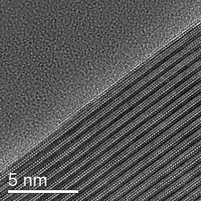
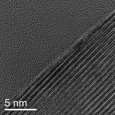
33 STEM-EELS OF MISCUT SAMPLES 33


34 Spectrum Imaging - areas One spectrum per pixel SiC SiO 2 Spectrum Image SiC SiO 2 HAADF Survey Image Simultaneous HAADF Signal 34


35 Spectrum Imaging - lines One spectrum per line SiC SiO 2 HAADF Survey Image Spectrum Image Lines 35
36 Si-L 2,3 chemical shift SiC SiO 2 1 D. Muller, Ultramicroscopy 78, 163 (1999). 36
37 Edge energy - SI 1 (ev) Si-L 2,3 chemical shift Track inflection point of edge onset across interface 1 Gradual and monotonic shift Si bonding changes gradually and uniformly across the interface Measured using rise/fall time calculations typical in signal processing Fall Time= Fall Range= Largest Triangle Position (nm) Example from new sample Si-O D. Muller, P. Batson, and J. Silcox, Physical Review B 58, (1998). 37
38 Samples investigated 2 x 3 matrix aimed at comparing substrate orientation (and miscut) with processing conditions: NO POA is for 2hr, all SiC substrates are n-type, SiO 2 ~60nm thick Sample Labels: Only oxidized NO Post-annealed Si-face on-axis Si-O 2-0 Si-N-0 Si-face miscut (4º ) Si-O 2-4 Si-N-4 a-face on-axis a-o 2-0 a-n-0 38


39 08/14/ J. Taillon/L. Salamanca-Riba Si-O2-4 Si-O2-0 a-o2-0 Si-N-4 Si-N-0 a-n-0 39
 40 cm 2 /Vs for Si-face 85 cm 2 /Vs for a-face")
40 w TL measurements Results from STEM EELS transition layer measurements show that w TL values are similar w TL in NO-annealed samples for these devices are actually slightly larger than the non-annealed a-face interfaces are the smallest, which does correspond with their higher mobilities (in NO) 40 cm 2 /Vs for Si-face 85 cm 2 /Vs for a-face 40
41 FUTURE WORK 41
.")

42 Roughness from HRTEM reconstructions Roughness of interface can be used to calculate power spectrum of interface Estimation of surface scattering-limited mobility possible from this 1,2 1 Goodnick, S., et al., Physical Review B, 32, (1985). 2 Zhao, Y., et al., IEEE Electron Device Letters, 30, (2009). How to measure? Difficult to digitize based on single image HRTEM focal series reconstruction allows extraction of pure wave function phase Could also accomplish this through electron holography 42

, 162 (2010).")
43 Strain measurement: geometric phase analysis Utilizing reconstructed phase, can measure strain captured in the interface Has been used to measure strain at misfit dislocations in Al-Pb interfaces 1 HRTEM Phase image Currently working on implementation of this method, but results are not ready yet 1 H. Rösner, C. T. Koch and G. Wilde, Acta Mater., 58(1), 162 (2010). Amplitude image Experimental quantitative strain map 1 43
44 Conclusions Spin-etch technique has been developed and used to do initial XPS profiles XPS results show some interesting leads for future investigation N bonding states, valence band differences, auger parameter of oxide STEM-EELS results on miscut samples show unexpected results that require additional thought/analysis Roughness and strain measurements at the SiC/SiO 2 interfaces in these samples are underway 44


45 Acknowledgements ARL Contracts W911NF and W911NF NSF Graduate Research Fellowship Grant DGE NISPLab at UMD supported by NSF and MRSEC Dr. Joshua Schumacher at NIST 45
46 THANK YOU Questions and comments? 46
The effectiveness of HCl and HF cleaning of Si 0.85 Ge 0.15 surface. Stanford Synchrotron Radiation Lab, Menlo Park, CA 94025
 July 2008 SLAC-PUB-13302 The effectiveness of HCl and HF cleaning of Si 0.85 Ge 0.15 surface Yun Sun, a) Zhi Liu, Shiyu Sun, Piero Pianetta Stanford Synchrotron Radiation Lab, Menlo Park, CA 94025 The
Atomic Level Analysis of SiC Devices Using Numerical Simulation
 Atomic Level Analysis of Devices Using Numerical mulation HIRSE, Takayuki MRI, Daisuke TERA, Yutaka ABSTRAT Research and development of power semiconductor devices with (silicon carbide) has been very
Effects of Antimony Near SiO 2 /SiC Interfaces
 Effects of Antimony Near SiO 2 /SiC Interfaces P.M. Mooney, A.F. Basile, and Zenan Jiang Simon Fraser University, Burnaby, BC, V5A1S6, Canada and Yongju Zheng, Tamara Isaacs-Smith Smith, Aaron Modic, and
UNIVERSITY OF CALIFORNIA College of Engineering Department of Electrical Engineering and Computer Sciences. Fall Exam 1
 UNIVERSITY OF CALIFORNIA College of Engineering Department of Electrical Engineering and Computer Sciences EECS 143 Fall 2008 Exam 1 Professor Ali Javey Answer Key Name: SID: 1337 Closed book. One sheet
Characterization of reliability-limiting defects in 4H-SiC MOSFETs using density functional (atomistic) simulations
 simulations") Characterization of reliability-limiting defects in 4H-SiC MOSFETs using density functional (atomistic) simulations Dev Ettisserry ARL Workshop 14, 15 August, 2014 UMD, College Park Advised by : Prof.
Characterization of reliability-limiting defects in 4H-SiC MOSFETs using density functional (atomistic) simulations Dev Ettisserry ARL Workshop 14, 15 August, 2014 UMD, College Park Advised by : Prof.
IV. Surface analysis for chemical state, chemical composition
 IV. Surface analysis for chemical state, chemical composition Probe beam Detect XPS Photon (X-ray) Photoelectron(core level electron) UPS Photon (UV) Photoelectron(valence level electron) AES electron
doi: /
 doi: 10.1063/1.350497 Morphology of hydrofluoric acid and ammonium fluoride-treated silicon surfaces studied by surface infrared spectroscopy M. Niwano, Y. Takeda, Y. Ishibashi, K. Kurita, and N. Miyamoto
QUESTIONS AND ANSWERS
 QUESTIONS AND ANSWERS (1) For a ground - state neutral atom with 13 protons, describe (a) Which element this is (b) The quantum numbers, n, and l of the inner two core electrons (c) The stationary state
Wide-gap Semiconducting Graphene from Nitrogen-seeded SiC
 Wide-gap Semiconducting Graphene from Nitrogen-seeded SiC F. Wang, 1 G. Liu, 2 S. Rothwell, 3 M. Nevius, 1 A. Tejeda, 4, 5 A. Taleb-Ibrahimi, 6 L.C. Feldman, 2 P.I. Cohen, 3 and E.H. Conrad 1 1 School
Local Anodic Oxidation of GaAs: A Nanometer-Scale Spectroscopic Study with PEEM
 Local Anodic Oxidation of GaAs: A Nanometer-Scale Spectroscopic Study with PEEM S. Heun, G. Mori, M. Lazzarino, D. Ercolani, G. Biasiol, and L. Sorba Laboratorio TASC-INFM, 34012 Basovizza, Trieste A.
Aberration-corrected TEM studies on interface of multilayered-perovskite systems
 Aberration-corrected TEM studies on interface of multilayered-perovskite systems By Lina Gunawan (0326114) Supervisor: Dr. Gianluigi Botton November 1, 2006 MSE 702(1) Presentation Outline Literature Review
Feature-level Compensation & Control. Process Integration September 15, A UC Discovery Project
 Feature-level Compensation & Control Process Integration September 15, 2005 A UC Discovery Project Current Milestones Si/Ge-on-insulator and Strained Si-on-insulator Substrate Engineering (M28 YII.13)
Auger Electron Spectroscopy Overview
 Auger Electron Spectroscopy Overview Also known as: AES, Auger, SAM 1 Auger Electron Spectroscopy E KLL = E K - E L - E L AES Spectra of Cu EdN(E)/dE Auger Electron E N(E) x 5 E KLL Cu MNN Cu LMM E f E
Auger Electron Spectroscopy
 Auger Electron Spectroscopy Auger Electron Spectroscopy is an analytical technique that provides compositional information on the top few monolayers of material. Detect all elements above He Detection
COTS BTS Testing and Improved Reliability Test Methods
 2015 August 2015 SiC MOS Program Review COTS BTS Testing and Improved Reliability Test Methods Aivars Lelis, Ron Green, Dan Habersat, and Mooro El Outline Lelis (and Green) : COTS BTS results Standard
Energy position of the active near-interface traps in metal oxide semiconductor field-effect transistors on 4H SiC
 Energy position of the active near-interface traps in metal oxide semiconductor field-effect transistors on 4H SiC Author Haasmann, Daniel, Dimitrijev, Sima Published 2013 Journal Title Applied Physics
Radiation Effects in Emerging Materials Overview Leonard C. Feldman
 May, 2010 Radia%on Effects on Emerging Electronic Materials and Devices Radiation Effects in Emerging Materials Overview Leonard C. Feldman Vanderbilt University And Rutgers University Ionizing radia%on
X-Ray Photoelectron Spectroscopy (XPS)-2
-2") X-Ray Photoelectron Spectroscopy (XPS)-2 Louis Scudiero http://www.wsu.edu/~scudiero; 5-2669 Fulmer 261A Electron Spectroscopy for Chemical Analysis (ESCA) The 3 step model: 1.Optical excitation 2.Transport
X-Ray Photoelectron Spectroscopy (XPS)-2 Louis Scudiero http://www.wsu.edu/~scudiero; 5-2669 Fulmer 261A Electron Spectroscopy for Chemical Analysis (ESCA) The 3 step model: 1.Optical excitation 2.Transport
Electronic Supplementary Information. Molecular Antenna Tailored Organic Thin-film Transistor for. Sensing Application
 Electronic Supplementary Material (ESI) for Materials Horizons. This journal is The Royal Society of Chemistry 2017 Electronic Supplementary Information Molecular Antenna Tailored Organic Thin-film Transistor
Lecture 150 Basic IC Processes (10/10/01) Page ECE Analog Integrated Circuits and Systems P.E. Allen
 Page ECE Analog Integrated Circuits and Systems P.E. Allen") Lecture 150 Basic IC Processes (10/10/01) Page 1501 LECTURE 150 BASIC IC PROCESSES (READING: TextSec. 2.2) INTRODUCTION Objective The objective of this presentation is: 1.) Introduce the fabrication of
Lecture 150 Basic IC Processes (10/10/01) Page 1501 LECTURE 150 BASIC IC PROCESSES (READING: TextSec. 2.2) INTRODUCTION Objective The objective of this presentation is: 1.) Introduce the fabrication of
Limiting Si/SiO 2 interface roughness resulting from thermal oxidation
 JOURNAL OF APPLIED PHYSICS VOLUME 86, NUMBER 3 1 AUGUST 1999 Limiting Si/SiO 2 interface roughness resulting from thermal oxidation L. Lai and E. A. Irene a) Department of Chemistry, University of North
Introduction to X-ray Photoelectron Spectroscopy (XPS) XPS which makes use of the photoelectric effect, was developed in the mid-1960
 XPS which makes use of the photoelectric effect, was developed in the mid-1960") Introduction to X-ray Photoelectron Spectroscopy (XPS) X-ray Photoelectron Spectroscopy (XPS), also known as Electron Spectroscopy for Chemical Analysis (ESCA) is a widely used technique to investigate
Introduction to X-ray Photoelectron Spectroscopy (XPS) X-ray Photoelectron Spectroscopy (XPS), also known as Electron Spectroscopy for Chemical Analysis (ESCA) is a widely used technique to investigate
Special Properties of Au Nanoparticles
 Special Properties of Au Nanoparticles Maryam Ebrahimi Chem 7500/750 March 28 th, 2007 1 Outline Introduction The importance of unexpected electronic, geometric, and chemical properties of nanoparticles
Lecture 23 X-Ray & UV Techniques
 Lecture 23 X-Ray & UV Techniques Schroder: Chapter 11.3 1/50 Announcements Homework 6/6: Will be online on later today. Due Wednesday June 6th at 10:00am. I will return it at the final exam (14 th June).
Effects of plasma treatment on the precipitation of fluorine-doped silicon oxide
 ARTICLE IN PRESS Journal of Physics and Chemistry of Solids 69 (2008) 555 560 www.elsevier.com/locate/jpcs Effects of plasma treatment on the precipitation of fluorine-doped silicon oxide Jun Wu a,, Ying-Lang
XPS Study of Ultrathin GeO 2 /Ge System
 XPS Study of Ultrathin GeO 2 /Ge System Akio Ohta, Hiroaki Furukawa, Hiroshi Nakagawa, Hideki Murakami, Seiichirou Higashi and Seiichi Miyazaki Graduate School of Adavanced Sciences of Matter, Hiroshima
Nanocrystalline Si formation inside SiN x nanostructures usingionized N 2 gas bombardment
 연구논문 한국진공학회지제 16 권 6 호, 2007 년 11 월, pp.474~478 Nanocrystalline Si formation inside SiN x nanostructures usingionized N 2 gas bombardment Min-Cherl Jung 1, Young Ju Park 2, Hyun-Joon Shin 1, Jun Seok Byun
X-Ray Photoelectron Spectroscopy (XPS)-2
-2") X-Ray Photoelectron Spectroscopy (XPS)-2 Louis Scudiero http://www.wsu.edu/~pchemlab ; 5-2669 Fulmer 261A Electron Spectroscopy for Chemical Analysis (ESCA) The 3 step model: 1.Optical excitation 2.Transport
X-Ray Photoelectron Spectroscopy (XPS)-2 Louis Scudiero http://www.wsu.edu/~pchemlab ; 5-2669 Fulmer 261A Electron Spectroscopy for Chemical Analysis (ESCA) The 3 step model: 1.Optical excitation 2.Transport
Supplementary Information
 Supplementary Information Supplementary Figures Supplementary figure S1: Characterisation of the electron beam intensity profile. (a) A 3D plot of beam intensity (grey value) with position, (b) the beam
Self-study problems and questions Processing and Device Technology, FFF110/FYSD13
 Self-study problems and questions Processing and Device Technology, FFF110/FYSD13 Version 2016_01 In addition to the problems discussed at the seminars and at the lectures, you can use this set of problems
Electronic structure of transition metal high-k dielectrics: interfacial band offset energies for microelectronic devices
 Applied Surface Science 212 213 (2003) 563 569 Electronic structure of transition metal high-k dielectrics: interfacial band offset energies for microelectronic devices Gerald Lucovsky *, Gilbert B. Rayner
Supplementary Information
 Supplementary Information Supplementary Figure 1. fabrication. A schematic of the experimental setup used for graphene Supplementary Figure 2. Emission spectrum of the plasma: Negative peaks indicate an
Birck Nanotechnology Center XPS: X-ray Photoelectron Spectroscopy ESCA: Electron Spectrometer for Chemical Analysis
 Birck Nanotechnology Center XPS: X-ray Photoelectron Spectroscopy ESCA: Electron Spectrometer for Chemical Analysis Dmitry Zemlyanov Birck Nanotechnology Center, Purdue University Outline Introduction
Energy Spectroscopy. Ex.: Fe/MgO
 Energy Spectroscopy Spectroscopy gives access to the electronic properties (and thus chemistry, magnetism,..) of the investigated system with thickness dependence Ex.: Fe/MgO Fe O Mg Control of the oxidation
Auger Electron Spectroscopy (AES) Prof. Paul K. Chu
 Prof. Paul K. Chu") Auger Electron Spectroscopy (AES) Prof. Paul K. Chu Auger Electron Spectroscopy Introduction Principles Instrumentation Qualitative analysis Quantitative analysis Depth profiling Mapping Examples The Auger
Auger Electron Spectroscopy (AES) Prof. Paul K. Chu Auger Electron Spectroscopy Introduction Principles Instrumentation Qualitative analysis Quantitative analysis Depth profiling Mapping Examples The Auger
Characterization of Charge Trapping and Dielectric Breakdown of HfAlOx/SiON Dielectric Gate Stack
 Characterization of Charge Trapping and Dielectric Breakdown of HfAlOx/SiON Dielectric Gate Stack Y. Pei, S. Nagamachi, H. Murakami, S. Higashi, S. Miyazaki, T. Kawahara and K. Torii Graduate School of
Electron Spectroscopy
 Electron Spectroscopy Photoelectron spectroscopy is based upon a single photon in/electron out process. The energy of a photon is given by the Einstein relation : E = h ν where h - Planck constant ( 6.62
DISTRIBUTION OF POTENTIAL BARRIER HEIGHT LOCAL VALUES AT Al-SiO 2 AND Si-SiO 2 INTERFACES OF THE METAL-OXIDE-SEMICONDUCTOR (MOS) STRUCTURES
 STRUCTURES") DISTRIBUTION OF POTENTIAL BARRIER HEIGHT LOCAL VALUES AT Al-SiO 2 AND Si-SiO 2 INTERFACES OF THE ETAL-OXIDE-SEICONDUCTOR (OS) STRUCTURES KRZYSZTOF PISKORSKI (kpisk@ite.waw.pl), HENRYK. PRZEWLOCKI Institute
DISTRIBUTION OF POTENTIAL BARRIER HEIGHT LOCAL VALUES AT Al-SiO 2 AND Si-SiO 2 INTERFACES OF THE ETAL-OXIDE-SEICONDUCTOR (OS) STRUCTURES KRZYSZTOF PISKORSKI (kpisk@ite.waw.pl), HENRYK. PRZEWLOCKI Institute
Electron capture and emission properties of interface states in thermally oxidized and NO-annealed SiO 2 /4H-SiC
 JOURNAL OF APPLIED PHYSICS 103, 033701 2008 Electron capture and emission properties of interface states in thermally oxidized and NO-annealed SiO 2 /4H-SiC X. D. Chen, 1,a S. Dhar, 2 T. Isaacs-Smith,
Cathodoluminescence spectroscopy of nitrided SiO 2 Si interfaces
 Cathodoluminescence spectroscopy of nitrided SiO 2 Si interfaces A. P. Young a) Department of Electrical Engineering, The Ohio State University, Columbus, Ohio 43210-1272 R. Bandhu Department of Physics,
Removal of Cu Impurities on a Si Substrate by Using (H 2 O 2 +HF) and (UV/O 3 +HF)
 and (UV/O 3 +HF)") Journal of the Korean Physical Society, Vol. 33, No. 5, November 1998, pp. 579 583 Removal of Cu Impurities on a Si Substrate by Using (H 2 O 2 +HF) and (UV/O 3 +HF) Baikil Choi and Hyeongtag Jeon School
Journal of the Korean Physical Society, Vol. 33, No. 5, November 1998, pp. 579 583 Removal of Cu Impurities on a Si Substrate by Using (H 2 O 2 +HF) and (UV/O 3 +HF) Baikil Choi and Hyeongtag Jeon School
Analysis of Nitrogen State on MOS Interface of 4H-SiC m-face after Nitric Oxide Post Oxidation Annealing (NO-POA)
") e-journal of Surface Science and Nanotechnology 31 October 2017 e-j. Surf. Sci. Nanotech. Vol. 15 (2017) 109-114 Regular Paper Analysis of Nitrogen State on MOS Interface of 4H-SiC m-face after Nitric
e-journal of Surface Science and Nanotechnology 31 October 2017 e-j. Surf. Sci. Nanotech. Vol. 15 (2017) 109-114 Regular Paper Analysis of Nitrogen State on MOS Interface of 4H-SiC m-face after Nitric
Fabrication Technology, Part I
 EEL5225: Principles of MEMS Transducers (Fall 2004) Fabrication Technology, Part I Agenda: Microfabrication Overview Basic semiconductor devices Materials Key processes Oxidation Thin-film Deposition Reading:
Name: (a) What core levels are responsible for the three photoelectron peaks in Fig. 1?
 What core levels are responsible for the three photoelectron peaks in Fig. 1?") Physics 243A--Surface Physics of Materials: Spectroscopy Final Examination December 16, 2014 (3 problems, 100 points total, open book, open notes and handouts) Name: [1] (50 points), including Figures
Physics 243A--Surface Physics of Materials: Spectroscopy Final Examination December 16, 2014 (3 problems, 100 points total, open book, open notes and handouts) Name: [1] (50 points), including Figures
Oxidation of hydrogenated crystalline silicon as an alternative approach for ultrathin SiO 2 growth
 Institute of Physics Publishing Journal of Physics: Conference Series 10 (2005) 246 250 doi:10.1088/1742-6596/10/1/061 Second Conference on Microelectronics, Microsystems and Nanotechnology Oxidation of
Traps in MOCVD n-gan Studied by Deep Level Transient Spectroscopy and Minority Carrier Transient Spectroscopy
 Traps in MOCVD n-gan Studied by Deep Level Transient Spectroscopy and Minority Carrier Transient Spectroscopy Yutaka Tokuda Department of Electrical and Electronics Engineering, Aichi Institute of Technology,
Supplementary Figure 1 Detailed illustration on the fabrication process of templatestripped
 Supplementary Figure 1 Detailed illustration on the fabrication process of templatestripped gold substrate. (a) Spin coating of hydrogen silsesquioxane (HSQ) resist onto the silicon substrate with a thickness
DEPOSITION OF THIN TiO 2 FILMS BY DC MAGNETRON SPUTTERING METHOD
 Chapter 4 DEPOSITION OF THIN TiO 2 FILMS BY DC MAGNETRON SPUTTERING METHOD 4.1 INTRODUCTION Sputter deposition process is another old technique being used in modern semiconductor industries. Sputtering
Reduced preferential sputtering of TiO 2 (and Ta 2 O 5 ) thin films through argon cluster ion bombardment.
 thin films through argon cluster ion bombardment.") NATIOMEM Reduced preferential sputtering of TiO 2 (and Ta 2 O 5 ) thin films through argon cluster ion bombardment. R. Grilli *, P. Mack, M.A. Baker * * University of Surrey, UK ThermoFisher Scientific
NATIOMEM Reduced preferential sputtering of TiO 2 (and Ta 2 O 5 ) thin films through argon cluster ion bombardment. R. Grilli *, P. Mack, M.A. Baker * * University of Surrey, UK ThermoFisher Scientific
A Plasmonic Photocatalyst Consisting of Silver Nanoparticles Embedded in Titanium Dioxide. Ryan Huschka LANP Seminar February 19, 2008
 A Plasmonic Photocatalyst Consisting of Silver Nanoparticles Embedded in Titanium Dioxide Ryan Huschka LANP Seminar February 19, 2008 TiO 2 Applications White Pigment Photocatalyst Previous methods to
Supplementary Figure S1. AFM characterizations and topographical defects of h- BN films on silica substrates. (a) (c) show the AFM height
 (c) show the AFM height") Supplementary Figure S1. AFM characterizations and topographical defects of h- BN films on silica substrates. (a) (c) show the AFM height topographies of h-bn film in a size of ~1.5µm 1.5µm, 30µm 30µm
Supplementary Figure S1. AFM characterizations and topographical defects of h- BN films on silica substrates. (a) (c) show the AFM height topographies of h-bn film in a size of ~1.5µm 1.5µm, 30µm 30µm
Auger Electron Spectrometry. EMSE-515 F. Ernst
 Auger Electron Spectrometry EMSE-515 F. Ernst 1 Principle of AES electron or photon in, electron out radiation-less transition Auger electron electron energy properties of atom 2 Brief History of Auger
Local Anodic Oxidation with AFM: A Nanometer-Scale Spectroscopic Study with Photoemission Microscopy
 Local Anodic Oxidation with AFM: A Nanometer-Scale Spectroscopic Study with Photoemission Microscopy S. Heun, G. Mori, M. Lazzarino, D. Ercolani,* G. Biasiol, and L. Sorba* Laboratorio Nazionale TASC-INFM,
Temperature Dependent Optical Band Gap Measurements of III-V films by Low Temperature Photoluminescence Spectroscopy
 Temperature Dependent Optical Band Gap Measurements of III-V films by Low Temperature Photoluminescence Spectroscopy Linda M. Casson, Francis Ndi and Eric Teboul HORIBA Scientific, 3880 Park Avenue, Edison,
Applications of XPS, AES, and TOF-SIMS
 Applications of XPS, AES, and TOF-SIMS Scott R. Bryan Physical Electronics 1 Materials Characterization Techniques Microscopy Optical Microscope SEM TEM STM SPM AFM Spectroscopy Energy Dispersive X-ray
Supporting information. Infrared Characterization of Interfacial Si-O Bond Formation on Silanized. Flat SiO 2 /Si Surfaces
 Supporting information Infrared Characterization of Interfacial Si-O Bond Formation on Silanized Flat SiO 2 /Si Surfaces Ruhai Tian,, Oliver Seitz, Meng Li, Wenchuang (Walter) Hu, Yves Chabal, Jinming
2D MBE Activities in Sheffield. I. Farrer, J. Heffernan Electronic and Electrical Engineering The University of Sheffield
 2D MBE Activities in Sheffield I. Farrer, J. Heffernan Electronic and Electrical Engineering The University of Sheffield Outline Motivation Van der Waals crystals The Transition Metal Di-Chalcogenides
Role of Electrochemical Reactions in the Degradation Mechanisms of AlGaN/GaN HEMTs
 Role of Electrochemical Reactions in the Degradation Mechanisms of AlGaN/GaN HEMTs Feng Gao 1,2, Bin Lu 2, Carl V. Thompson 1, Jesús del Alamo 2, Tomás Palacios 2 1. Department of Materials Science and
X- ray Photoelectron Spectroscopy and its application in phase- switching device study
 X- ray Photoelectron Spectroscopy and its application in phase- switching device study Xinyuan Wang A53073806 I. Background X- ray photoelectron spectroscopy is of great importance in modern chemical and
X-ray photoelectron spectroscopy - An introduction
 X-ray photoelectron spectroscopy - An introduction Spyros Diplas spyros.diplas@sintef.no spyros.diplas@smn.uio.no SINTEF Materials & Chemistry, Materials Physics -Oslo & Centre of Materials Science and
Optimizing Graphene Morphology on SiC(0001)
") Optimizing Graphene Morphology on SiC(0001) James B. Hannon Rudolf M. Tromp Graphene sheets Graphene sheets can be formed into 0D,1D, 2D, and 3D structures Chemically inert Intrinsically high carrier mobility
Optimizing Graphene Morphology on SiC(0001) James B. Hannon Rudolf M. Tromp Graphene sheets Graphene sheets can be formed into 0D,1D, 2D, and 3D structures Chemically inert Intrinsically high carrier mobility
Surface and Electronic Structure Study of Substrate-dependent Pyrite Thin Films
 Surface and Electronic Structure Study of Substrate-dependent Pyrite Thin Films Talk Outline Stoichiometry and sodium study of pyrite thin films: Quick Review Surface structure of pyrite thin films Electronic
Shu Hu 1,2, Matthias H. Richter 1,2, Michael F. Lichterman 1,2, Joseph Beardslee 2,4, Thomas Mayer 5, Bruce S. Brunschwig 1 and Nathan S.
 Supporting Information for: Electrical, Photoelectrochemical and Photoelectron Spectroscopic Investigation of the Interfacial Transport and Energetics of Amorphous TiO 2 /Si Heterojunctions Shu Hu 1,2,
Photoemission Spectroscopy
 FY13 Experimental Physics - Auger Electron Spectroscopy Photoemission Spectroscopy Supervisor: Per Morgen SDU, Institute of Physics Campusvej 55 DK - 5250 Odense S Ulrik Robenhagen,
Investigation of the bonding strength and interface current of p-siõn-gaas wafers bonded by surface activated bonding at room temperature
 Investigation of the bonding strength and interface current of p-siõn-gaas wafers bonded by surface activated bonding at room temperature M. M. R. Howlader, a) T. Watanabe, and T. Suga Research Center
J. Price, 1,2 Y. Q. An, 1 M. C. Downer 1 1 The university of Texas at Austin, Department of Physics, Austin, TX
 Understanding process-dependent oxygen vacancies in thin HfO 2 /SiO 2 stacked-films on Si (100) via competing electron-hole injection dynamic contributions to second harmonic generation. J. Price, 1,2
NBTI and Spin Dependent Charge Pumping in 4H-SiC MOSFETs
 NBTI and Spin Dependent Charge Pumping in 4H-SiC MOSFETs Mark A. Anders, Patrick M. Lenahan, Pennsylvania State University Aivars Lelis, US Army Research Laboratory Energy Deviations from the resonance
(a) (b) Supplementary Figure 1. (a) (b) (a) Supplementary Figure 2. (a) (b) (c) (d) (e)
 (b) Supplementary Figure 1. (a) (b) (a) Supplementary Figure 2. (a) (b) (c) (d) (e)") (a) (b) Supplementary Figure 1. (a) An AFM image of the device after the formation of the contact electrodes and the top gate dielectric Al 2 O 3. (b) A line scan performed along the white dashed line
(a) (b) Supplementary Figure 1. (a) An AFM image of the device after the formation of the contact electrodes and the top gate dielectric Al 2 O 3. (b) A line scan performed along the white dashed line
Supporting Information. Direct n- to p-type Channel Conversion in Monolayer/Few-Layer WS 2 Field-Effect Transistors by Atomic Nitrogen Treatment
 Supporting Information Direct n- to p-type Channel Conversion in Monolayer/Few-Layer WS 2 Field-Effect Transistors by Atomic Nitrogen Treatment Baoshan Tang 1,2,, Zhi Gen Yu 3,, Li Huang 4, Jianwei Chai
Spin-resolved photoelectron spectroscopy
 Spin-resolved photoelectron spectroscopy Application Notes Spin-resolved photoelectron spectroscopy experiments were performed in an experimental station consisting of an analysis and a preparation chamber.
Surface and Interface Characterization of Polymer Films
 Surface and Interface Characterization of Polymer Films Jeff Shallenberger, Evans Analytical Group 104 Windsor Center Dr., East Windsor NJ Copyright 2013 Evans Analytical Group Outline Introduction to
SUPPLEMENTARY INFORMATION
 SUPPLEMENTARY INFORMATION Facile Synthesis of High Quality Graphene Nanoribbons Liying Jiao, Xinran Wang, Georgi Diankov, Hailiang Wang & Hongjie Dai* Supplementary Information 1. Photograph of graphene
Atomic configuration of boron pile-up at the Si/SiO 2 interface
 Atomic configuration of boron pile-up at the Si/SiO 2 interface Masayuki Furuhashi, a) Tetsuya Hirose, Hiroshi Tsuji, Masayuki Tachi, and Kenji Taniguchi Department of Electronics and Information Systems,
ATOMIC-SCALE THEORY OF RADIATION-INDUCED PHENOMENA
 ATOMIC-SCALE THEORY OF RADIATION-INDUCED PHENOMENA OVERVIEW OF THE LAST FIVE YEARS AND NEW RESULTS Sokrates T. Pantelides Department of Physics and Astronomy, Vanderbilt University, Nashville, TN The theory
Supporting Information
 Supporting Information Improved Stability of Atomic Layer Deposited Amorphous TiO 2 Photoelectrode Coatings by Thermally Induced Oxygen Defects Markku Hannula, Harri Ali-Löytty, Kimmo Lahtonen, Essi Sarlin,
Lecture 7 Chemical/Electronic Structure of Glass
 Lecture 7 Chemical/Electronic Structure of Glass Syllabus Topic 6. Electronic spectroscopy studies of glass structure Fundamentals and Applications of X-ray Photoelectron Spectroscopy (XPS) a.k.a. Electron
High Resolution Photoemission Study of the Spin-Dependent Band Structure of Permalloy and Ni
 High Resolution Photoemission Study of the Spin-Dependent Band Structure of Permalloy and Ni K. N. Altmann, D. Y. Petrovykh, and F. J. Himpsel Department of Physics, University of Wisconsin, Madison, 1150
Photon Energy Dependence of Contrast in Photoelectron Emission Microscopy of Si Devices
 Photon Energy Dependence of Contrast in Photoelectron Emission Microscopy of Si Devices V. W. Ballarotto, K. Siegrist, R. J. Phaneuf, and E. D. Williams University of Maryland and Laboratory for Physical
Depth profile study of ferroelectric PbZr 0.2 Ti 0.8 O 3 films
 JOURNAL OF APPLIED PHYSICS VOLUME 92, NUMBER 11 1 DECEMBER 2002 Depth profile study of ferroelectric PbZr 0.2 Ti 0.8 O 3 films Y. Li, V. Nagarajan, S. Aggarwal, R. Ramesh, L. G. Salamanca-Riba, and L.
Supporting Information
 Electronic Supplementary Material (ESI) for Nanoscale. This journal is The Royal Society of Chemistry 2015 Supporting Information Single Layer Lead Iodide: Computational Exploration of Structural, Electronic
Formation mechanism and Coulomb blockade effect in self-assembled gold quantum dots
 Formation mechanism and Coulomb blockade effect in self-assembled gold quantum dots S. F. Hu a) National Nano Device Laboratories, Hsinchu 300, Taiwan R. L. Yeh and R. S. Liu Department of Chemistry, National
Methods of surface analysis
 Methods of surface analysis Nanomaterials characterisation I RNDr. Věra Vodičková, PhD. Surface of solid matter: last monoatomic layer + absorbed monolayer physical properties are effected (crystal lattice
Figure 1: Graphene release, transfer and stacking processes. The graphene stacking began with CVD
 Supplementary figure 1 Graphene Growth and Transfer Graphene PMMA FeCl 3 DI water Copper foil CVD growth Back side etch PMMA coating Copper etch in 0.25M FeCl 3 DI water rinse 1 st transfer DI water 1:10
Monolayer Semiconductors
 Monolayer Semiconductors Gilbert Arias California State University San Bernardino University of Washington INT REU, 2013 Advisor: Xiaodong Xu (Dated: August 24, 2013) Abstract Silicon may be unable to
Inversion of wurtzite GaN(0001) by exposure to magnesium
 by exposure to magnesium") Inversion of wurtzite GaN(0001) by exposure to magnesium V. Ramachandran and R. M. Feenstra Department of Physics, Carnegie Mellon University, Pittsburgh, PA 15213 W. L. Sarney and L. Salamanca-Riba Materials
Inversion of wurtzite GaN(0001) by exposure to magnesium V. Ramachandran and R. M. Feenstra Department of Physics, Carnegie Mellon University, Pittsburgh, PA 15213 W. L. Sarney and L. Salamanca-Riba Materials
X-ray photoelectron spectroscopy - An introduction
 X-ray photoelectron spectroscopy - An introduction Spyros Diplas SINTEF Materials & Chemistry, Sector of Materials and Nanotechnology, Department of Materials Physics-Oslo & Centre of Materials Science
Supplementary Information. Experimental Evidence of Exciton Capture by Mid-Gap Defects in CVD. Grown Monolayer MoSe2
 Supplementary Information Experimental Evidence of Exciton Capture by Mid-Gap Defects in CVD Grown Monolayer MoSe2 Ke Chen 1, Rudresh Ghosh 2,3, Xianghai Meng 1, Anupam Roy 2,3, Joon-Seok Kim 2,3, Feng
UNIT 3. By: Ajay Kumar Gautam Asst. Prof. Dev Bhoomi Institute of Technology & Engineering, Dehradun
 UNIT 3 By: Ajay Kumar Gautam Asst. Prof. Dev Bhoomi Institute of Technology & Engineering, Dehradun 1 Syllabus Lithography: photolithography and pattern transfer, Optical and non optical lithography, electron,
Paper presentation. M S Bootha Raju Date: 28/11/09
 Paper presentation M S Bootha Raju Date: 28/11/09 Photoemission Spectroscopy and Atomic Force Microscopy Investigation of Vapor-Phase Codeposited Silver/Poly(3-hexylthiophene) Composites L. Scudiero, Haoyan
Supporting Information
 Electronic Supplementary Material (ESI) for Physical Chemistry Chemical Physics. This journal is the Owner Societies 2014 Supporting Information A direct Fe-O coordination at FePc/MoO x interface investigated
LECTURE 5 SUMMARY OF KEY IDEAS
 LECTURE 5 SUMMARY OF KEY IDEAS Etching is a processing step following lithography: it transfers a circuit image from the photoresist to materials form which devices are made or to hard masking or sacrificial
Characterization of Secondary Emission Materials for Micro-Channel Plates. S. Jokela, I. Veryovkin, A. Zinovev
 Characterization of Secondary Emission Materials for Micro-Channel Plates S. Jokela, I. Veryovkin, A. Zinovev Secondary Electron Yield Testing Technique We have incorporated XPS, UPS, Ar-ion sputtering,
UNIVERSITY OF CALIFORNIA College of Engineering Department of Electrical Engineering and Computer Sciences. Professor Chenming Hu.
 UNIVERSITY OF CALIFORNIA College of Engineering Department of Electrical Engineering and Computer Sciences EECS 130 Spring 2009 Professor Chenming Hu Midterm I Name: Closed book. One sheet of notes is
SUPPLEMENTARY INFORMATION
 Lateral heterojunctions within monolayer MoSe 2 -WSe 2 semiconductors Chunming Huang 1,#,*, Sanfeng Wu 1,#,*, Ana M. Sanchez 2,#,*, Jonathan J. P. Peters 2, Richard Beanland 2, Jason S. Ross 3, Pasqual
PHI 5000 Versaprobe-II Focus X-ray Photo-electron Spectroscopy
 PHI 5000 Versaprobe-II Focus X-ray Photo-electron Spectroscopy The very basic theory of XPS XPS theroy Surface Analysis Ultra High Vacuum (UHV) XPS Theory XPS = X-ray Photo-electron Spectroscopy X-ray
Normally-Off GaN Field Effect Power Transistors: Device Design and Process Technology Development
 Center for High Performance Power Electronics Normally-Off GaN Field Effect Power Transistors: Device Design and Process Technology Development Dr. Wu Lu (614-292-3462, lu.173@osu.edu) Dr. Siddharth Rajan
X-Ray Photoelectron Spectroscopy (XPS) Prof. Paul K. Chu
 Prof. Paul K. Chu") X-Ray Photoelectron Spectroscopy (XPS) Prof. Paul K. Chu X-ray Photoelectron Spectroscopy Introduction Qualitative analysis Quantitative analysis Charging compensation Small area analysis and XPS imaging
X-Ray Photoelectron Spectroscopy (XPS) Prof. Paul K. Chu X-ray Photoelectron Spectroscopy Introduction Qualitative analysis Quantitative analysis Charging compensation Small area analysis and XPS imaging
Electronic Supporting Information for
 Electronic Supplementary Material (ESI) for Materials Horizons. This journal is The Royal Society of Chemistry 2015 Electronic Supporting Information for Probing the Energy Levels in Hole-doped Molecular
Characterization of Post-etch Residue Clean By Chemical Bonding Transformation Mapping
 Characterization of Post-etch Residue Clean By Chemical Bonding Transformation Mapping Muthappan Asokan, Oliver Chyan*, Interfacial Electrochemistry and Materials Research Lab, University of North Texas
The surface activation layer of GaAs negative electron affinity photocathode activated by
 SLAC-PUB-13810 The surface activation layer of GaAs negative electron affinity photocathode activated by Cs, Li and NF 3 Y. Sun 1, a), R.E. Kirby 2, T. Maruyama 3, G. A. Mulhollan 2, J. C. Bierman 2 and