Chun Ning Lau (Jeanie) Graphene: Quantum Transport in a 2D Membrane
|
|
|
- Melvin Allison
- 5 years ago
- Views:
Transcription
")

1 Chun Ning Lau (Jeanie) Graphene: Quantum Transport in a 2D Membrane

2 Grapheneʼs Double Identity Extraordinary Conductor 2D Elastic Membrane Novoselov et al Nature 2005; Zhang et al, Nature New model system for condensed matter research and electronic materials Linear dispersion, tunable carrier, surface 2DEG, high thermal and electrical conductivity. Thinnest isolated membrane with exceptional mechanical properties

 50 0-50 -80V -4-2 0 2 4 Gate")
3 Outline Quantum Transport of charges Tunable pn junctions Graphene as a 2D membrane A new wrinkle V(µV) I(nA) V Gate Voltage (V)


4 Extraction of Single- and Bi-Layer Graphene Single-layer graphene Optical Microscope Bi-layer graphene AFM 5 µm 1-layer 2-layer layer 2µm Mechanical exfoliation -- rub graphite flakes onto SiO 2 substrates Identify the number of layers by Raman spectroscopy Transport measurement Color contrast in an optical microscope AFM images reveal mesoscopic features
 Supercurrent carried by electrons, holes and in nominally undoped regimes. Critical current depends on gate voltage. Miao, Bao, Zhang, CNL, Solid State Comm.")
5 Graphene Supercurrent Transistor Weak link 10 nm Ti + 70 nm Al SC SC 500 V(µV) 50 V g 50 V (µv) 0 I c I (na) V g (V) I (na) Supercurrent carried by electrons, holes and in nominally undoped regimes. Critical current depends on gate voltage. Miao, Bao, Zhang, CNL, Solid State Comm.(2009)
6 Graphene p-n Junctions Unique advantage: local control of charge density and type Graphene p-n junctions with top gate(s): allow in situ tuning of junction polarity and dopant levels Application Klein tunneling (perfect transmission of relativistic particles across high barrier) recent evidence: Kim s group, Goldhaber-Gordon s group, & Savchenko s group. Veselago lensing (optics-like focusing of electron rays) Band gap engineering of bi-layer graphene Particle collimation Valley polarization Theories: Abanin et al 2006, 2007; Fogler et al 2007; Shytov et al 2007; Katsnelson et al 2006; Beenakker group, Cheianov et al 2006, 2007 Experimental demonstration: Huard et al 2007; Williams et al 2007, Ozyilmaz et al 2007, Oostinga et al 2007
. Cheianov and Falko, PRB (2006).")

7 Klein Tunneling Relativistic charged particles at normal incidence has perfect transmission across a high barrier (V 0 >~ 2 mc 2 ). Cheianov and Falko, PRB (2006). Katsnelson et al, Nature Physics (2006). Thought to be realizable at the edge of blackholes Graphene: electrons in conduction band holes in valence band Transmission probability depends on incidence angle

8 Graphene p-n Junctions Challenge: deposition of top gate tends to dope or damage the atomic layer Innovation: Suspended, contactless top gate Gentle process Graphene can be annealed to improve mobility and contact Graphene Electrode Suspended gate V g Top gate Graphene V A
 50 Individual control of charge density and type of different regions Liu, Velasco Jr.")
9 Conductance of p-n-p Junctions npn pp p R(kΩ) nn n pnp Dirac point of the bare region R(kΩ) 10 5 V tg =14 V V tg =-14 V V tg =28 V Dirac point of the top gated region V bg (V) 50 Individual control of charge density and type of different regions Liu, Velasco Jr. and Lau, APL (2008); see also Gorbachev et al, Nano Letter (2008).
.")
 = 2π \"n 2 = 4 #n 2 L slope of linear fit: ~ 1 x 10 5 /cm L ~ 740 nm width")
10 Fabry Perot Interference R(kΩ) R(kΩ) Young and Kim, Nature Physics (2009); Shytov, Levitov et al, arxiv (2008). Fabry Perot Interference of holes at pn interferences between successive peaks k F (2L) = 2π "n 2 = 4 #n 2 L slope of linear fit: ~ 1 x 10 5 /cm L ~ 740 nm width of top gate ~ 500 nm, distance from substrate ~ 100 nm
 G(e 2")
 1.5 1.0 0 V tg (V) 6/5 2/3 20 G. Liu, J. Velasco Jr, C.N.")
11 Quantum Hall States in graphene p-n-p Junctions Quantum Hall plateau at fractional values of e 2 /h Edge state equilibration, full mixing of propagation modes at interfaces Full and partial edge state equilibration ν 2 ν 1 p p p Edge State B=8T transmission G = e2 h min ( " 1," 2 ) G(e 2 /h) ν 2 > ν 1 p p p Partial Equilibration G = e2 h " 1 " 2 2" 1 # " p n p Marcus group, Science (2007). Abanin & Levitov, Science (2007). Full Equilibration G = e2 h " 1 " 2 2" 1 + " 2 Ozyilmaz et al, PRL 2007 G (e 2 /h) V tg (V) 6/5 2/3 20 G. Liu, J. Velasco Jr, C.N. Lau, APL (2008)

12 Future Work Spin transport in p-n junctions Junction shape Abanine & Levitov, PRB, 2008; Cheianov et al 2006, 2007, Fogler et al, 2008; Zhang & Fogler, Veselago Lensing (requires extremely clean devices suspended graphene + suspended gate?) Supercurrent in p-n junctions
13 Grapheneʼs Double Identity Extraordinary Conductor The Softer Side of Graphene Novoselov et al Nature 2005; Zhang et al, Nature Collaborator: Chris Dames, New model system for condensed matter research and electronic materials Linear dispersion, tunable carrier, surface 2DEG, high thermal and electrical conductivity. Thinnest isolated membrane with exceptional mechanical properties
14 Ripples in Graphene Presence of ripples in suspended graphene inferred from electron diffraction patterns Significant implication on electrical transport properties induce local gauge field change local chemical potential ultimate bottleneck for mobility? (Theories by Louie, Castro Neto, Katnelson, Guinea, Herbut et al, Juan et al ) Meyer et al, Nature (2007) No direct observation of ripples
 Exfoliate graphene onto substrates Deposit electrodes Release completed devices")

 metal electrodes trench Electrode")
15 (Attempts to) Fabricate Suspended Graphene Devices Successful Technique (Kim and Andrei groups, 2008) Exfoliate graphene onto substrates Deposit electrodes Release completed devices from SiO 2 using HF etching Anneal Observed much higher mobility (up to 250,000) Our technique Etch trenches on substrates trench Directly exfoliate graphene sheets across trenches Deposit electrodes Anneal Initial test: very low mobility (~ ) our typical substrate-supported devices: ~ 2,000-10,000 Du et al, Nature Physics (2008) metal electrodes trench Electrode graphene trench

16 Huh? Jeanie read the map!


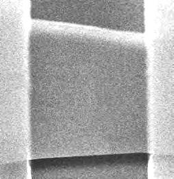
17 Imaging Suspended Graphene Directly exfoliate graphene sheets across pre-defined trenches Image under SEM trench graphene substrate 5µm 2µm 5µm Titl angle = 0º 45º >75º


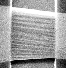
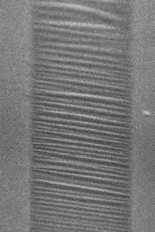
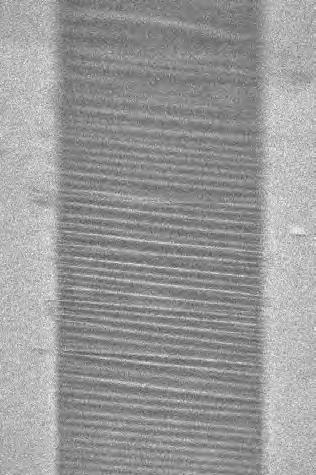
18 Spontaneous, Periodic Ripple Formation in Graphene Directly exfoliate graphene sheets across pre-defined trenches Many graphene sheets are not flat, but spontaneously form ripples Almost perfectly sinusoidal profile thickness: 0.3 nm (single layer) nm amplitude: 0.7 to 30 nm wavelength: 370 nm -- 5 µm SEM AFM substrate substrate 1 µm Distance (µm)
19 Origin of Ripples competition between bending and stretching ripples can be induced by longitudinal strains or E shears A" L = 8# 3(1$ # 2 ) t in-plane shear 15 A" L = 8 3(1+ #) t in-plane strain A!/L (nm) A=amplitude, L=length, λ=wavelength, t=thickness, ν=poisson ratio ~ t (nm) 20
 t in-plane strain A!/L (nm) A=amplitude, L=length, λ=wavelength, t=thickness, ν=poisson ratio~0.")
20 Graphene as an Elastic Membrane competition between bending and stretching ripples induced by longitudinal strains or shears E A" L = 8# 3(1$ # 2 ) t in-plane shear 15 Data from 51 samples A" L = 8 3(1+ #) t in-plane strain A!/L (nm) A=amplitude, L=length, λ=wavelength, t=thickness, ν=poisson ratio~ t (nm) 20
21 Strain-Induced Ripples in Atomic Membranes 1 single layer bi-layer 3-layer theory Aλ/L (nm) A!/L (nm) t (nm) 0 0 t (nm) 2 strain " = 4# 2 ( ) 3 1$% 2 ( tl) 2 & 4 t (nm) Membranes that are a few atomic layers thick obeys thin film mechanics Larger range of strains (up to 2%) observed for thinner membranes


22 Graphene as the World s thinnest Saran Wrap macroscopic mesoscopic 1 µm


23 Device Fabrication Attempt Ripples are the culprits for low mobility of our devices? Not so fast! Devices were annealed to improve mobility 300 ºC 1µm 1µm 2µm 2µm graphene sheets collapsed


24 Thermal Effect on Ripples 250 ºC 300 ºC 5µm Ripples have larger wavelengths and amplitudes Membranes buckles upward or towards the bottom of the trench


25 In Situ SEM imaging of ripple formation 1 µm T=25C 300C 25C 25C 300C 25C 2 µm

26 Movie of ripple formation


27 Mechanism of ripple formation Graphene has a negative thermal expansion coefficient Heating graphene contracts, substrate expands erasing pre-existing ripples Cooling graphene expands, substrate contracts bending is easier than sliding edges remain pinned by the trench edges ripples (transverse) slacks (longitudinal)
/L t (T) at different temperatures Slope b = dl dt \" #$ # Si Bao, Miao,Chen, Zhang, Jung, Dames and CNL, Nature Nanotechnol.")
28 Measurement of Thermal Expansion Coefficient α L t L g Single layer graphene heated to 500 K and cools down slowly Compute l(t)=l g (T)/L t (T) at different temperatures Slope b = dl dt " #$ # Si Bao, Miao,Chen, Zhang, Jung, Dames and CNL, Nature Nanotechnol. (2009)


29 Ongoing: Cooling Suspended Graphene 300K 100K 300K


30 Ongoing: Electrostatic Distortion of Suspended Graphene Gate Voltage = 0V 10V Gate voltages induces deformation in suspended graphene membranes. 20V 30V Back to 0V Leon, Prada, San-Jose, Guinea, PRL (2009)
31 Lessons Learnt Always look at the devices Suspended graphene membranes are very finicky! often have ripples anneal with care collapse graphene cause ripples to form or change morphology is strongly temperature dependent resistance is strongly temperature dependent quantum Hall plateaus disappear after annealing nanoelectromechanical resonatorʼs characteristic frequency shifts with temperature shape changes with gate voltages
32 Grapheneʼs Double Identity Extraordinary Conductor 2D Elastic Membrane New model system for condensed matter research and electronic materials Linear dispersion, tunable carrier, surface 2DEG, high thermal and electrical conductivity. Thinnest isolated membrane with exceptional mechanical properties Castro Neto, Guinea, Katsnelson, Brey, Louie, etc Exploit Electrical Properties of Rippled Graphene? superlattices, strain-based engineering


33 Coming soon -- Electrical Measurement Device with random or periodic ripples suspended and substrate supported portions of the same graphene sheet 2µm 5µm suspended with small ripples on-substrate very low mobility Despite small random ripples, suspended graphene has higher mobility Collapsed graphene (with very severe strain) does have very low mobility Ripple s T-dependence: relevant for suspended graphene devices


34 Acknowledgments Graduate Students Feng Miao Wenzhong Bao Discussion With Shan-Wan Tsai, Marc Bockrath, Antonio Castro-Neto, Misha Fogler, Paco Guinea, Gil Refael, Dmitri Abanin, Philip Kim, Chandra Varma, Leonid Pryadko, Dmitri Novikov, Alex Bratkosvki, Volodya Falko, Maria A.H. Vozmediano, Misha Katsnelson Gang Liu Jairo Velasco Hang Zhang
Chun Ning Lau (Jeanie) Graphene Quantum Electronics: p-n Junctions and Atomic Switches
 Graphene Quantum Electronics: p-n Junctions and Atomic Switches") Chun Ning Lau (Jeanie) Graphene Quantum Electronics: p-n Junctions and Atomic Switches Acknowledgement Graduate Students Feng Miao Wenzhong Bao Discussion With Shan-Wan Tsai, Antonio Castro-Neto, Michael
Chun Ning Lau (Jeanie) Graphene Quantum Electronics: p-n Junctions and Atomic Switches Acknowledgement Graduate Students Feng Miao Wenzhong Bao Discussion With Shan-Wan Tsai, Antonio Castro-Neto, Michael
Electrical transport in high-quality graphene pnp junctions
 Electrical transport in high-quality graphene pnp junctions To cite this article: Jairo Velasco Jr et al 2009 New J. Phys. 11 095008 View the article online for updates and enhancements. Related content
SUPPLEMENTARY INFORMATION
 SUPPLEMENTARY INFORMATION Controlled Ripple Texturing of Suspended Graphene and Ultrathin Graphite Membranes Wenzhong Bao, Feng Miao, Zhen Chen, Hang Zhang, Wanyoung Jang, Chris Dames, Chun Ning Lau *
Lithography-free Fabrication of High Quality Substrate-supported and. Freestanding Graphene devices
 Lithography-free Fabrication of High Quality Substrate-supported and Freestanding Graphene devices W. Bao 1, G. Liu 1, Z. Zhao 1, H. Zhang 1, D. Yan 2, A. Deshpande 3, B.J. LeRoy 3 and C.N. Lau 1, * 1
Lithography-Free Fabrication of High Quality Substrate- Supported and Freestanding Graphene Devices
 98 DOI 10.1007/s12274-010-1013-5 Research Article Lithography-Free Fabrication of High Quality Substrate- Supported and Freestanding Graphene Devices Wenzhong Bao 1, Gang Liu 1, Zeng Zhao 1, Hang Zhang
Bilayer graphene (BLG) is a unique two-dimensional
 is a unique two-dimensional") Quantum Transport and Field-Induced Insulating States in Bilayer Graphene pnp Junctions Lei Jing, Jairo Velasco Jr., Philip Kratz, Gang Liu, Wenzhong Bao, Marc Bockrath, and Chun Ning Lau* Department of
Quantum Transport and Field-Induced Insulating States in Bilayer Graphene pnp Junctions Lei Jing, Jairo Velasco Jr., Philip Kratz, Gang Liu, Wenzhong Bao, Marc Bockrath, and Chun Ning Lau* Department of
Transport through Andreev Bound States in a Superconductor-Quantum Dot-Graphene System
 Transport through Andreev Bound States in a Superconductor-Quantum Dot-Graphene System Nadya Mason Travis Dirk, Yung-Fu Chen, Cesar Chialvo Taylor Hughes, Siddhartha Lal, Bruno Uchoa Paul Goldbart University
Klein tunneling in graphene p-n-p junctions
 10.1149/1.3569920 The Electrochemical Society Klein tunneling in graphene p-n-p junctions E. Rossi 1,J.H.Bardarson 2,3,P.W.Brouwer 4 1 Department of Physics, College of William and Mary, Williamsburg,
Quantum Hall Effect in Graphene p-n Junctions
 Quantum Hall Effect in Graphene p-n Junctions Dima Abanin (MIT) Collaboration: Leonid Levitov, Patrick Lee, Harvard and Columbia groups UIUC January 14, 2008 Electron transport in graphene monolayer New
Ambipolar Graphene Field Effect Transistors by Local Metal Side Gates USA. Indiana 47907, USA. Abstract
 Ambipolar Graphene Field Effect Transistors by Local Metal Side Gates J. F. Tian *, a, b, L. A. Jauregui c, b, G. Lopez c, b, H. Cao a, b *, a, b, c, and Y. P. Chen a Department of Physics, Purdue University,
SUPPLEMENTARY INFORMATION
 SUPPLEMENTARY INFORMATION SUPPLEMENTARY INFORMATION Trilayer graphene is a semimetal with a gate-tuneable band overlap M. F. Craciun, S. Russo, M. Yamamoto, J. B. Oostinga, A. F. Morpurgo and S. Tarucha
(a) (b) Supplementary Figure 1. (a) (b) (a) Supplementary Figure 2. (a) (b) (c) (d) (e)
 (b) Supplementary Figure 1. (a) (b) (a) Supplementary Figure 2. (a) (b) (c) (d) (e)") (a) (b) Supplementary Figure 1. (a) An AFM image of the device after the formation of the contact electrodes and the top gate dielectric Al 2 O 3. (b) A line scan performed along the white dashed line
(a) (b) Supplementary Figure 1. (a) An AFM image of the device after the formation of the contact electrodes and the top gate dielectric Al 2 O 3. (b) A line scan performed along the white dashed line
Graphene Field effect transistors
 GDR Meso 2008 Aussois 8-11 December 2008 Graphene Field effect transistors Jérôme Cayssol CPMOH, UMR Université de Bordeaux-CNRS 1) Role of the contacts in graphene field effect transistors motivated by
Chun Ning Lau (Jeanie) Quantum Transport! in! 2D Atomic Membranes!
 Quantum Transport! in! 2D Atomic Membranes!") Chun Ning Lau (Jeanie) Quantum Transport! in! 2D Atomic Membranes! 2D Materials and Heterostructures! hbn MoS 2 WSe 2 Fluorographene Geim, Nature 2013. Conductors, e.g. graphene, few-layer graphene Semiconductors,
Chun Ning Lau (Jeanie) Quantum Transport! in! 2D Atomic Membranes! 2D Materials and Heterostructures! hbn MoS 2 WSe 2 Fluorographene Geim, Nature 2013. Conductors, e.g. graphene, few-layer graphene Semiconductors,
Supplementary Figure S1. AFM images of GraNRs grown with standard growth process. Each of these pictures show GraNRs prepared independently,
 Supplementary Figure S1. AFM images of GraNRs grown with standard growth process. Each of these pictures show GraNRs prepared independently, suggesting that the results is reproducible. Supplementary Figure
Supplementary information for Tunneling Spectroscopy of Graphene-Boron Nitride Heterostructures
 Supplementary information for Tunneling Spectroscopy of Graphene-Boron Nitride Heterostructures F. Amet, 1 J. R. Williams, 2 A. G. F. Garcia, 2 M. Yankowitz, 2 K.Watanabe, 3 T.Taniguchi, 3 and D. Goldhaber-Gordon
Graphene: : CERN on the desk. Mikhail Katsnelson
 Graphene: : CERN on the desk Mikhail Katsnelson Instead of epigraph You can get much further with a kind word and a gun than you can with a kind word alone (Al Capone) You can get much further with an
Lecture 3: Heterostructures, Quasielectric Fields, and Quantum Structures
 Lecture 3: Heterostructures, Quasielectric Fields, and Quantum Structures MSE 6001, Semiconductor Materials Lectures Fall 2006 3 Semiconductor Heterostructures A semiconductor crystal made out of more
Overview. Carbon in all its forms. Background & Discovery Fabrication. Important properties. Summary & References. Overview of current research
 Graphene Prepared for Solid State Physics II Pr Dagotto Spring 2009 Laurene Tetard 03/23/09 Overview Carbon in all its forms Background & Discovery Fabrication Important properties Overview of current
KAVLI v F. Curved graphene revisited. María A. H. Vozmediano. Instituto de Ciencia de Materiales de Madrid CSIC
 KAVLI 2012 v F Curved graphene revisited María A. H. Vozmediano Instituto de Ciencia de Materiales de Madrid CSIC Collaborators ICMM(Graphene group) http://www.icmm.csic.es/gtg/ A. Cano E. V. Castro J.
Graphene A One-Atom-Thick Material for Microwave Devices
 ROMANIAN JOURNAL OF INFORMATION SCIENCE AND TECHNOLOGY Volume 11, Number 1, 2008, 29 35 Graphene A One-Atom-Thick Material for Microwave Devices D. DRAGOMAN 1, M. DRAGOMAN 2, A. A. MÜLLER3 1 University
Suspended graphene: a bridge to the Dirac point.
 Suspended graphene: a bridge to the Dirac point. Xu Du, Ivan Skachko, Anthony Barker, Eva Y. Andrei Department of Physics & Astronomy, Rutgers the State University of New Jersey The recent discovery of
Effects of Interactions in Suspended Graphene
 Effects of Interactions in Suspended Graphene Ben Feldman, Andrei Levin, Amir Yacoby, Harvard University Broken and unbroken symmetries in the lowest LL: spin and valley symmetries. FQHE Discussions with
Black phosphorus: A new bandgap tuning knob
 Black phosphorus: A new bandgap tuning knob Rafael Roldán and Andres Castellanos-Gomez Modern electronics rely on devices whose functionality can be adjusted by the end-user with an external knob. A new
Optimizing Graphene Morphology on SiC(0001)
") Optimizing Graphene Morphology on SiC(0001) James B. Hannon Rudolf M. Tromp Graphene sheets Graphene sheets can be formed into 0D,1D, 2D, and 3D structures Chemically inert Intrinsically high carrier mobility
Optimizing Graphene Morphology on SiC(0001) James B. Hannon Rudolf M. Tromp Graphene sheets Graphene sheets can be formed into 0D,1D, 2D, and 3D structures Chemically inert Intrinsically high carrier mobility
Graphene - most two-dimensional system imaginable
 Graphene - most two-dimensional system imaginable A suspended sheet of pure graphene a plane layer of C atoms bonded together in a honeycomb lattice is the most two-dimensional system imaginable. A.J.
SUPPLEMENTARY INFORMATION
 Collapse of superconductivity in a hybrid tin graphene Josephson junction array by Zheng Han et al. SUPPLEMENTARY INFORMATION 1. Determination of the electronic mobility of graphene. 1.a extraction from
SiC Graphene Suitable For Quantum Hall Resistance Metrology.
 SiC Graphene Suitable For Quantum Hall Resistance Metrology. Samuel Lara-Avila 1, Alexei Kalaboukhov 1, Sara Paolillo, Mikael Syväjärvi 3, Rositza Yakimova 3, Vladimir Fal'ko 4, Alexander Tzalenchuk 5,
Graphene. Tianyu Ye November 30th, 2011
 Graphene Tianyu Ye November 30th, 2011 Outline What is graphene? How to make graphene? (Exfoliation, Epitaxial, CVD) Is it graphene? (Identification methods) Transport properties; Other properties; Applications;
ICTP Conference Graphene Week 2008
 1960-3 ICTP Conference Graphene Week 2008 25-29 August 2008 Current-induced cleaning of graphene J. Moser CIN2 Barcelona, Campus UAB, Bellaterra, Spain A. Barreiro CIN2 Barcelona, Campus UAB, Bellaterra,
Graphene electronics
 Graphene electronics Alberto Morpurgo Main collaborators J. Oostinga, H. Heersche, P. Jarillo Herrero, S. Russo, M. Craciun, L. Vandersypen, S. Tarucha, R. Danneau, P. Hakkonen A simple tight-binding H
TRANSVERSE SPIN TRANSPORT IN GRAPHENE
 International Journal of Modern Physics B Vol. 23, Nos. 12 & 13 (2009) 2641 2646 World Scientific Publishing Company TRANSVERSE SPIN TRANSPORT IN GRAPHENE TARIQ M. G. MOHIUDDIN, A. A. ZHUKOV, D. C. ELIAS,
Fermi Level Pinning at Electrical Metal Contacts. of Monolayer Molybdenum Dichalcogenides
 Supporting information Fermi Level Pinning at Electrical Metal Contacts of Monolayer Molybdenum Dichalcogenides Changsik Kim 1,, Inyong Moon 1,, Daeyeong Lee 1, Min Sup Choi 1, Faisal Ahmed 1,2, Seunggeol
Broken Symmetry States and Divergent Resistance in Suspended Bilayer Graphene
 Broken Symmetry States and Divergent Resistance in Suspended Bilayer Graphene The Harvard community has made this article openly available. Please share how this access benefits you. Your story matters.
Supporting Information. Nanoscale control of rewriteable doping patterns in pristine graphene/boron nitride heterostructures
 Supporting Information Nanoscale control of rewriteable doping patterns in pristine graphene/boron nitride heterostructures Jairo Velasco Jr. 1,5,, Long Ju 1,, Dillon Wong 1,, Salman Kahn 1, Juwon Lee
Supporting Information. by Hexagonal Boron Nitride
 Supporting Information High Velocity Saturation in Graphene Encapsulated by Hexagonal Boron Nitride Megan A. Yamoah 1,2,, Wenmin Yang 1,3, Eric Pop 4,5,6, David Goldhaber-Gordon 1 * 1 Department of Physics,
Graphene: massless electrons in flatland.
 Graphene: massless electrons in flatland. Enrico Rossi Work supported by: University of Chile. Oct. 24th 2008 Collaorators CMTC, University of Maryland Sankar Das Sarma Shaffique Adam Euyuong Hwang Roman
SUPPLEMENTARY INFORMATION
 Dirac electron states formed at the heterointerface between a topological insulator and a conventional semiconductor 1. Surface morphology of InP substrate and the device Figure S1(a) shows a 10-μm-square
Observation of topological surface state quantum Hall effect in an intrinsic three-dimensional topological insulator
 Observation of topological surface state quantum Hall effect in an intrinsic three-dimensional topological insulator Authors: Yang Xu 1,2, Ireneusz Miotkowski 1, Chang Liu 3,4, Jifa Tian 1,2, Hyoungdo
Supplementary Figure 1. Selected area electron diffraction (SAED) of bilayer graphene and tblg. (a) AB
 of bilayer graphene and tblg. (a) AB") Supplementary Figure 1. Selected area electron diffraction (SAED) of bilayer graphene and tblg. (a) AB stacked bilayer graphene (b), (c), (d), (e), and (f) are twisted bilayer graphene with twist angle
Supplementary Figure 1. Selected area electron diffraction (SAED) of bilayer graphene and tblg. (a) AB stacked bilayer graphene (b), (c), (d), (e), and (f) are twisted bilayer graphene with twist angle
A BIT OF MATERIALS SCIENCE THEN PHYSICS
 GRAPHENE AND OTHER D ATOMIC CRYSTALS Andre Geim with many thanks to K. Novoselov, S. Morozov, D. Jiang, F. Schedin, I. Grigorieva, J. Meyer, M. Katsnelson A BIT OF MATERIALS SCIENCE THEN PHYSICS CARBON
Supplementary Figure 2 Photoluminescence in 1L- (black line) and 7L-MoS 2 (red line) of the Figure 1B with illuminated wavelength of 543 nm.
 and 7L-MoS 2 (red line) of the Figure 1B with illuminated wavelength of 543 nm.") PL (normalized) Intensity (arb. u.) 1 1 8 7L-MoS 1L-MoS 6 4 37 38 39 4 41 4 Raman shift (cm -1 ) Supplementary Figure 1 Raman spectra of the Figure 1B at the 1L-MoS area (black line) and 7L-MoS area (red
PL (normalized) Intensity (arb. u.) 1 1 8 7L-MoS 1L-MoS 6 4 37 38 39 4 41 4 Raman shift (cm -1 ) Supplementary Figure 1 Raman spectra of the Figure 1B at the 1L-MoS area (black line) and 7L-MoS area (red
A. Optimizing the growth conditions of large-scale graphene films
 1 A. Optimizing the growth conditions of large-scale graphene films Figure S1. Optical microscope images of graphene films transferred on 300 nm SiO 2 /Si substrates. a, Images of the graphene films grown
Ferromagnetism and Anomalous Hall Effect in Graphene
 Ferromagnetism and Anomalous Hall Effect in Graphene Jing Shi Department of Physics & Astronomy, University of California, Riverside Graphene/YIG Introduction Outline Proximity induced ferromagnetism Quantized
SUPPLEMENTARY INFORMATION
 Dirac cones reshaped by interaction effects in suspended graphene D. C. Elias et al #1. Experimental devices Graphene monolayers were obtained by micromechanical cleavage of graphite on top of an oxidized
Properties of suspended graphene membranes
 Properties of suspended graphene membranes Graphene, a single layer of graphite, is a unique two-dimensional electron system as well as nature s thinnest elastic membrane. Here we review and describe our
Carbon based Nanoscale Electronics
 Carbon based Nanoscale Electronics 09 02 200802 2008 ME class Outline driving force for the carbon nanomaterial electronic properties of fullerene exploration of electronic carbon nanotube gold rush of
Imaging electrostatically confined Dirac fermions in graphene
 Imaging electrostatically confined Dirac fermions in graphene quantum dots 3 4 5 Juwon Lee, Dillon Wong, Jairo Velasco Jr., Joaquin F. Rodriguez-Nieva, Salman Kahn, Hsin- Zon Tsai, Takashi Taniguchi, Kenji
Supplementary Figure 1 Dark-field optical images of as prepared PMMA-assisted transferred CVD graphene films on silicon substrates (a) and the one
 and the one") Supplementary Figure 1 Dark-field optical images of as prepared PMMA-assisted transferred CVD graphene films on silicon substrates (a) and the one after PBASE monolayer growth (b). 1 Supplementary Figure
Supplementary Figure 1 Dark-field optical images of as prepared PMMA-assisted transferred CVD graphene films on silicon substrates (a) and the one after PBASE monolayer growth (b). 1 Supplementary Figure
Electronic Doping and Scattering by Transition Metals on Graphene
 Electronic Doping and Scattering by Transition Metals on Graphene K. Pi,* K. M. McCreary,* W. Bao, Wei Han, Y. F. Chiang, Yan Li, S.-W. Tsai, C. N. Lau, and R. K. Kawakami Department of Physics and Astronomy,
2D Materials for Gas Sensing
 2D Materials for Gas Sensing S. Guo, A. Rani, and M.E. Zaghloul Department of Electrical and Computer Engineering The George Washington University, Washington DC 20052 Outline Background Structures of
GRAPHENE the first 2D crystal lattice
 GRAPHENE the first 2D crystal lattice dimensionality of carbon diamond, graphite GRAPHENE realized in 2004 (Novoselov, Science 306, 2004) carbon nanotubes fullerenes, buckyballs what s so special about
Xu Du, Ivan Skachko and Eva Y. Andrei
 International Journal of Modern Physics B World Scientific Publishing Company TOWARDS BALLISTIC TRANSPORT IN GRAPHENE Xu Du, Ivan Skachko and Eva Y. Andrei Department of Physics and Astronomy, Rutgers
Graphite, graphene and relativistic electrons
 Graphite, graphene and relativistic electrons Introduction Physics of E. graphene Y. Andrei Experiments Rutgers University Transport electric field effect Quantum Hall Effect chiral fermions STM Dirac
Electrical Characteristics of Multilayer MoS 2 FET s
 Electrical Characteristics of Multilayer MoS 2 FET s with MoS 2 /Graphene Hetero-Junction Contacts Joon Young Kwak,* Jeonghyun Hwang, Brian Calderon, Hussain Alsalman, Nini Munoz, Brian Schutter, and Michael
Graphene and Quantum Hall (2+1)D Physics
D Physics") The 4 th QMMRC-IPCMS Winter School 8 Feb 2011, ECC, Seoul, Korea Outline 2 Graphene and Quantum Hall (2+1)D Physics Lecture 1. Electronic structures of graphene and bilayer graphene Lecture 2. Electrons
The 4 th QMMRC-IPCMS Winter School 8 Feb 2011, ECC, Seoul, Korea Outline 2 Graphene and Quantum Hall (2+1)D Physics Lecture 1. Electronic structures of graphene and bilayer graphene Lecture 2. Electrons
Supporting Information
 Electronic Supplementary Material (ESI) for ChemComm. This journal is The Royal Society of Chemistry 2014 Supporting Information Controllable Atmospheric Pressure Growth of Mono-layer, Bi-layer and Tri-layer
Graphene The Search For Two Dimensions. Christopher Scott Friedline Arizona State University
 Graphene The Search For Two Dimensions Christopher Scott Friedline Arizona State University What Is Graphene? Single atomic layer of graphite arranged in a honeycomb crystal lattice Consists of sp 2 -bonded
graphene nano-optoelectronics Frank Koppens ICFO, The institute of photonic sciences, Barcelona
 graphene nano-optoelectronics Frank Koppens ICFO, The institute of photonic sciences, Barcelona Graphene research at ICFO Frank Koppens: group Nano-optoelectronics (~100% graphene) Nano-optics and plasmonics
Piezoresistive Sensors
 Piezoresistive Sensors Outline Piezoresistivity of metal and semiconductor Gauge factor Piezoresistors Metal, silicon and polysilicon Close view of the piezoresistivity of single crystal silicon Considerations
Raman Imaging and Electronic Properties of Graphene
 Raman Imaging and Electronic Properties of Graphene F. Molitor, D. Graf, C. Stampfer, T. Ihn, and K. Ensslin Laboratory for Solid State Physics, ETH Zurich, 8093 Zurich, Switzerland ensslin@phys.ethz.ch
GRAPHENE ON THE Si-FACE OF SILICON CARBIDE USER MANUAL
 GRAPHENE ON THE Si-FACE OF SILICON CARBIDE USER MANUAL 1. INTRODUCTION Silicon Carbide (SiC) is a wide band gap semiconductor that exists in different polytypes. The substrate used for the fabrication
NiCl2 Solution concentration. Etching Duration. Aspect ratio. Experiment Atmosphere Temperature. Length(µm) Width (nm) Ar:H2=9:1, 150Pa
 Width (nm) Ar:H2=9:1, 150Pa") Experiment Atmosphere Temperature #1 # 2 # 3 # 4 # 5 # 6 # 7 # 8 # 9 # 10 Ar:H2=9:1, 150Pa Ar:H2=9:1, 150Pa Ar:H2=9:1, 150Pa Ar:H2=9:1, 150Pa Ar:H2=9:1, 150Pa Ar:H2=9:1, 150Pa Ar:H2=9:1, 150Pa Ar:H2=9:1,
Experiment Atmosphere Temperature #1 # 2 # 3 # 4 # 5 # 6 # 7 # 8 # 9 # 10 Ar:H2=9:1, 150Pa Ar:H2=9:1, 150Pa Ar:H2=9:1, 150Pa Ar:H2=9:1, 150Pa Ar:H2=9:1, 150Pa Ar:H2=9:1, 150Pa Ar:H2=9:1, 150Pa Ar:H2=9:1,
Terahertz sensing and imaging based on carbon nanotubes:
 Terahertz sensing and imaging based on carbon nanotubes: Frequency-selective detection and near-field imaging Yukio Kawano RIKEN, JST PRESTO ykawano@riken.jp http://www.riken.jp/lab-www/adv_device/kawano/index.html
SUPPLEMENTARY INFORMATION
 Supplementary Information: Photocurrent generation in semiconducting and metallic carbon nanotubes Maria Barkelid 1*, Val Zwiller 1 1 Kavli Institute of Nanoscience, Delft University of Technology, Delft,
Transport properties through double-magnetic-barrier structures in graphene
 Chin. Phys. B Vol. 20, No. 7 (20) 077305 Transport properties through double-magnetic-barrier structures in graphene Wang Su-Xin( ) a)b), Li Zhi-Wen( ) a)b), Liu Jian-Jun( ) c), and Li Yu-Xian( ) c) a)
& Dirac Fermion confinement Zahra Khatibi
 Graphene & Dirac Fermion confinement Zahra Khatibi 1 Outline: What is so special about Graphene? applications What is Graphene? Structure Transport properties Dirac fermions confinement Necessity External
TOPOLOGICAL BANDS IN GRAPHENE SUPERLATTICES
 TOPOLOGICAL BANDS IN GRAPHENE SUPERLATTICES 1) Berry curvature in superlattice bands 2) Energy scales for Moire superlattices 3) Spin-Hall effect in graphene Leonid Levitov (MIT) @ ISSP U Tokyo MIT Manchester
Fabrication of graphene nanogap with crystallographically matching edges and its. electron emission properties
 Fabrication of graphene nanogap with crystallographically matching edges and its electron emission properties H. M. Wang, 1 Z. Zheng, 1 Y.Y.Wang, 1 J.J. Qiu, Z.B. Guo, Z. X. Shen, 1 and T. Yu 1,* 1 Division
Surfaces, Interfaces, and Layered Devices
 Surfaces, Interfaces, and Layered Devices Building blocks for nanodevices! W. Pauli: God made solids, but surfaces were the work of Devil. Surfaces and Interfaces 1 Interface between a crystal and vacuum
Elastic properties of graphene
 Elastic properties of graphene M. I. Katsnelson P. Le Doussal B. Horowitz K. Wiese J. Gonzalez P. San-Jose V. Parente B. Amorim R. Roldan C. Gomez-Navarro J. Gomez G. Lopez-Polin F. Perez-Murano A. Morpurgo
1. Nanotechnology & nanomaterials -- Functional nanomaterials enabled by nanotechnologies.
 Novel Nano-Engineered Semiconductors for Possible Photon Sources and Detectors NAI-CHANG YEH Department of Physics, California Institute of Technology 1. Nanotechnology & nanomaterials -- Functional nanomaterials
Klein Tunneling. PHYS 503 Physics Colloquium Fall /11
 Klein Tunneling PHYS 503 Physics Colloquium Fall 2008 9/11 Deeak Rajut Graduate Research Assistant Center for Laser Alications University of Tennessee Sace Institute Email: drajut@utsi.edu Web: htt://drajut.com
crystals were phase-pure as determined by x-ray diffraction. Atomically thin MoS 2 flakes were
 Nano Letters (214) Supplementary Information for High Mobility WSe 2 p- and n-type Field Effect Transistors Contacted by Highly Doped Graphene for Low-Resistance Contacts Hsun-Jen Chuang, Xuebin Tan, Nirmal
Precision Cutting and Patterning of Graphene with Helium Ions. 1.School of Engineering and Applied Sciences, Harvard University, Cambridge MA 02138
 Precision Cutting and Patterning of Graphene with Helium Ions D.C. Bell 1,2, M.C. Lemme 3, L. A. Stern 4, J.R. Williams 1,3, C. M. Marcus 3 1.School of Engineering and Applied Sciences, Harvard University,
From nanophysics research labs to cell phones. Dr. András Halbritter Department of Physics associate professor
 From nanophysics research labs to cell phones Dr. András Halbritter Department of Physics associate professor Curriculum Vitae Birth: 1976. High-school graduation: 1994. Master degree: 1999. PhD: 2003.
Frictional characteristics of exfoliated and epitaxial graphene
 Frictional characteristics of exfoliated and epitaxial graphene Young Jun Shin a,b, Ryan Stromberg c, Rick Nay c, Han Huang d, Andrew T. S. Wee d, Hyunsoo Yang a,b,*, Charanjit S. Bhatia a a Department
Spring College on Computational Nanoscience May Electric Transport in Carbon Nanotubes and Graphene
 145-8 Spring College on Computational Nanoscience 17-8 May 1 Electric Transport in Carbon Nanotubes and Graphene Philip KIM Dept. of Physics, Columbia University New York U.S.A. Electric Transport in Nanotubes
Gate-induced insulating state in bilayer graphene devices
 Gate-induced insulating state in bilayer graphene devices Jeroen B. Oostinga, Hubert B. Heersche, Xinglan Liu, Alberto F. Morpurgo and Lieven M. K. Vandersypen Kavli Institute of Nanoscience, Delft University
Self-study problems and questions Processing and Device Technology, FFF110/FYSD13
 Self-study problems and questions Processing and Device Technology, FFF110/FYSD13 Version 2016_01 In addition to the problems discussed at the seminars and at the lectures, you can use this set of problems
Observation of an Electric-Field Induced Band Gap in Bilayer Graphene by Infrared Spectroscopy. Cleveland, OH 44106, USA
 Observation of an Electric-Field Induced Band Gap in Bilayer Graphene by Infrared Spectroscopy Kin Fai Mak 1, Chun Hung Lui 1, Jie Shan 2, and Tony F. Heinz 1* 1 Departments of Physics and Electrical Engineering,
Initial Stages of Growth of Organic Semiconductors on Graphene
 Initial Stages of Growth of Organic Semiconductors on Graphene Presented by: Manisha Chhikara Supervisor: Prof. Dr. Gvido Bratina University of Nova Gorica Outline Introduction to Graphene Fabrication
From graphene to Z2 topological insulator
 From graphene to Z2 topological insulator single Dirac topological AL mass U U valley WL ordinary mass or ripples WL U WL AL AL U AL WL Rashba Ken-Ichiro Imura Condensed-Matter Theory / Tohoku Univ. Dirac
Supporting Online Material for
 www.sciencemag.org/cgi/content/full/320/5874/356/dc1 Supporting Online Material for Chaotic Dirac Billiard in Graphene Quantum Dots L. A. Ponomarenko, F. Schedin, M. I. Katsnelson, R. Yang, E. W. Hill,
Electric Field-Dependent Charge-Carrier Velocity in Semiconducting Carbon. Nanotubes. Yung-Fu Chen and M. S. Fuhrer
 Electric Field-Dependent Charge-Carrier Velocity in Semiconducting Carbon Nanotubes Yung-Fu Chen and M. S. Fuhrer Department of Physics and Center for Superconductivity Research, University of Maryland,
SUPPLEMENTARY INFORMATION. Observation of tunable electrical bandgap in large-area twisted bilayer graphene synthesized by chemical vapor deposition
 SUPPLEMENTARY INFORMATION Observation of tunable electrical bandgap in large-area twisted bilayer graphene synthesized by chemical vapor deposition Jing-Bo Liu 1 *, Ping-Jian Li 1 *, Yuan-Fu Chen 1, Ze-Gao
1. Theoretical predictions for charged impurity scattering in graphene
 Supplementary Information 1. Theoretical predictions for charged impurity scattering in graphene We briefly review the state of theoretical and experimental work on zeromagnetic-field charge transport
NONLOCAL TRANSPORT IN GRAPHENE: VALLEY CURRENTS, HYDRODYNAMICS AND ELECTRON VISCOSITY
 NONLOCAL TRANSPORT IN GRAPHENE: VALLEY CURRENTS, HYDRODYNAMICS AND ELECTRON VISCOSITY Leonid Levitov (MIT) Frontiers of Nanoscience ICTP Trieste, August, 2015 Boris @ 60 2 Boris @ 60 3 Boris Blinks the
2D MBE Activities in Sheffield. I. Farrer, J. Heffernan Electronic and Electrical Engineering The University of Sheffield
 2D MBE Activities in Sheffield I. Farrer, J. Heffernan Electronic and Electrical Engineering The University of Sheffield Outline Motivation Van der Waals crystals The Transition Metal Di-Chalcogenides
Tunable Graphene Single Electron Transistor
 Tunable Graphene Single Electron Transistor NANO LETTERS 2008 Vol. 8, No. 8 2378-2383 C. Stampfer,* E. Schurtenberger, F. Molitor, J. Güttinger, T. Ihn, and K. Ensslin Solid State Physics Laboratory, ETH
Graphene and Carbon Nanotubes
 Graphene and Carbon Nanotubes 1 atom thick films of graphite atomic chicken wire Novoselov et al - Science 306, 666 (004) 100μm Geim s group at Manchester Novoselov et al - Nature 438, 197 (005) Kim-Stormer
Supplementary Information
 Supplementary Information Supplementary Figure 1 AFM and Raman characterization of WS 2 crystals. (a) Optical and AFM images of a representative WS 2 flake. Color scale of the AFM image represents 0-20
Topological insulator (TI)
") Topological insulator (TI) Haldane model: QHE without Landau level Quantized spin Hall effect: 2D topological insulators: Kane-Mele model for graphene HgTe quantum well InAs/GaSb quantum well 3D topological
Topological insulator (TI) Haldane model: QHE without Landau level Quantized spin Hall effect: 2D topological insulators: Kane-Mele model for graphene HgTe quantum well InAs/GaSb quantum well 3D topological
Supplementary Figure 1: Micromechanical cleavage of graphene on oxygen plasma treated Si/SiO2. Supplementary Figure 2: Comparison of hbn yield.
 1 2 3 4 Supplementary Figure 1: Micromechanical cleavage of graphene on oxygen plasma treated Si/SiO 2. Optical microscopy images of three examples of large single layer graphene flakes cleaved on a single
vapour deposition. Raman peaks of the monolayer sample grown by chemical vapour
 Supplementary Figure 1 Raman spectrum of monolayer MoS 2 grown by chemical vapour deposition. Raman peaks of the monolayer sample grown by chemical vapour deposition (S-CVD) are peak which is at 385 cm
state spectroscopy Xing Lan Liu, Dorothee Hug, Lieven M. K. Vandersypen Netherlands
 Gate-defined graphene double quantum dot and excited state spectroscopy Xing Lan Liu, Dorothee Hug, Lieven M. K. Vandersypen Kavli Institute of Nanoscience, Delft University of Technology, P.O. Box 5046,
Quantum Hall effect in graphene
 Solid State Communications 143 (2007) 14 19 www.elsevier.com/locate/ssc Quantum Hall effect in graphene Z. Jiang a,b, Y. Zhang a, Y.-W. Tan a, H.L. Stormer a,c, P. Kim a, a Department of Physics, Columbia
Controlling Graphene Ultrafast Hot Carrier Response from Metal-like. to Semiconductor-like by Electrostatic Gating
 Controlling Graphene Ultrafast Hot Carrier Response from Metal-like to Semiconductor-like by Electrostatic Gating S.-F. Shi, 1,2* T.-T. Tang, 1 B. Zeng, 1 L. Ju, 1 Q. Zhou, 1 A. Zettl, 1,2,3 F. Wang 1,2,3
GRAPHENE NANORIBBONS Nahid Shayesteh,
 USC Department of Physics Graduate Seminar 1 GRAPHENE NANORIBBONS Nahid Shayesteh, Outlines 2 Carbon based material Discovery and innovation of graphen Graphene nanoribbons structure Application of Graphene
Graphene Fundamentals and Emergent Applications
 Graphene Fundamentals and Emergent Applications Jamie H. Warner Department of Materials University of Oxford Oxford, UK Franziska Schaffel Department of Materials University of Oxford Oxford, UK Alicja