Physics 736. Experimental Methods in Nuclear-, Particle-, and Astrophysics
|
|
|
- Archibald Hancock
- 5 years ago
- Views:
Transcription
1 Physics 736 Experimental Methods in Nuclear-, Particle-, and Astrophysics - Ionization & Semiconductor Detectors - Karsten Heeger heeger@wisc.edu
2 Homework #6 Is due on Friday March 22 at 4.30pm
3 Make-up Lecture Friday March 22 at 4.40pm
4 Review of Last Lecture? Q: What determines the energy resolution in ionization detectors? Karsten Heeger, Univ. of Wisconsin Physics 736, Spring 2011
5 Review of Last Lecture? Q: What are the physics/detector characteristics that characterize ionization detectors? Karsten Heeger, Univ. of Wisconsin Physics 736, Spring 2011
6 Review of Last Lecture? Q: What are the physics/detector characteristics that characterize ionization detectors? diffusion drift velocity mobility energy resolution multiplication, gain Karsten Heeger, Univ. of Wisconsin Physics 736, Spring 2011
7 Ionization Detectors Avalanche formation Positive I ion drill I Id Electron 1 drift Anode Wire Q: why is avalanche drop shaped? Karsten Heeger, Univ. of Wisconsin Physics 736, Spring 2011

8 Ionization Detectors Avalanche formation Positive I ion drill I Id Electron 1 drift Anode Wire electrons are more mobile than ions Karsten Heeger, Univ. of Wisconsin Physics 736, Spring 2011
9 Review of Last Lecture What is a Townsend coefficient?

10 Review of Last Lecture What is a Townsend coefficient? Threshold for gas multiplicalion Eleclnc field strength
11 Ionization Detectors Operating Regions of Ionization Detectors trcoarbimtioa 1 bdcr coircfon f.gao C linit 4 d proportbmll' 5! a o t E lo' o o o, 3 to' z lonholio 2?roporfioncl 3 ; chorb.r Goutl'.? : i-r-i I I -l II Nr 7 II o rorlkl I Oirbrgr 6 rgfco I p F ttd n Vottoge, rcltr Karsten Heeger, Univ. of Wisconsin Physics 736, Spring 2011

12 Ionization Detectors Operating Regions of Ionization Detectors trcoarbimtioa bdcr coircfon f.gao C linit d proportbmll'! a o t E lo' o o o, 3 to' z lonholio?roporfioncl ; chorb.r Goutl'.? : i-r-i I I -l II Nr 7 II o rorlkl I Oirbrgr rgfco I p F ttd n Vottoge, rcltr Karsten Heeger, Univ. of Wisconsin Physics 736, Spring 2011

13 Ionization Detectors Proportional Counter Karsten Heeger, Univ. of Wisconsin Physics 736, Spring 2011
14 Homework #6 - Key Concepts TPC drift, diffusion, ionization, scintillation. electron-ion recombination
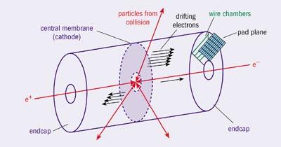
15 TPC
16 Homework #6 Q: What difference does it make whether you drift ions or electrons? - in terms of diffusion? - in terms of signal detection?
17 Homework #6 Q: What difference does it make whether you drift ions or electrons? - in terms of diffusion? diffusion can be much smaller for ions - in terms of signal detection? positively charged ions cannot induce avalanches
18 Homework #6 Q: What are the forms of energy transfer to Xenon atoms?
19 Homework #6 Q: What are the forms of energy transfer to Xenon atoms?
20 Homework #6 Q: What about Xenon and Fano factor?
21 Semiconductor Detectors
22 Review of Semiconductor Detectors What distinguishes a semiconductor from an insulator or conductor?
23 Review of Semiconductor Detectors What distinguishes a semiconductor from an insulator or conductor? What is the typical energy gap of a semiconductor?

24 Semiconductor Detectors Energy Band Structure En =6.eV Conduction band Energy 9ap valence band electrons Valence band Insutator Semiconductor Metat

25 Semiconductor Detectors Energy Band Structure En =6.eV Conduction band Energy 9ap valence band electrons Valence band Insutator Semiconductor Metat

26 Semiconductor Detectors Energy Band Structure
 at 0 K, all clectrons participate in bonding, (b) at higher temperatur6 some bonds are broken by thcrmal encrgy leaving a hole in the")
27 Semiconductor Detectors Covalent Bonding of Silicon T=0K T=300K (a) Valence electrons Semiconductor atom Free elcctron (b) Hole +o -i i. J I- *rt#'. o Fb. f0.2. Covalcnt bonding of silicon: (r) at 0 K, all clectrons participate in bonding, (b) at higher temperatur6 some bonds are broken by thcrmal encrgy leaving a hole in the valence band

28 Semiconductor Detectors Recombination and Trapping Conduction bend Ccntcr Vrlencc band Flg Rccombination and trapping sites in the forbidden energy gap

29 Semiconductor Detectors Recombination and Trapping
30 Semiconductor Detectors Doped Semiconductors n-type semiconductor donor impurities p-type semiconductor acceptor impurities "Excess" electron 0onor impurity "Excess" hote Acceptor impurity (a) Donor impurity level (b) Acceptor impurity level excess of electrons excess of holes

31 Semiconductor Detectors Doped Semiconductors n-type semiconductor donor impurities p-type semiconductor acceptor impurities

32 Semiconductor Detectors pn junction without bias

33 Semiconductor Detectors pn junction without bias

34 Semiconductor Detectors np Junction oa oa oo,, l -l!l lrj I


35 Semiconductor Detectors np junction structure for np junction structure of np junction when current applied When a current is driven through the np junction in the forward direction the electrons drop through the valence band to the empty electron states In a laser this energy drop can either be by the process of spontaneous or stimulated emission of a photon
36 Semiconductor Detectors np junction and diode laser np semiconductor is the laser medium where stimulated emission occurs

37 Semiconductor Detectors np junction and diode laser


38 Semiconductor Detectors reverse bias junction no applied voltage reverse bias enlarges sensitive volume for radiation detection reverse bias holes in the P-type material are pulled away from the junction, causing the width of the depletion zone to increase. 1 Deptetion I l-- Zone.+l with Bias Depletion Zone without Bias lir iit ;rf

39 Semiconductor Detectors junction diode detector Bias Metal contact heavily doped n + layer with almost zero depletion zone => ohmic contact

40 Semiconductor Detectors position sensitive detector uses resistive charge division low-resistive electrode on back charge collected at B will be proportional to energy of particle and resistance of electrode between contact and point of incidence x= L x B/C method of resistive charge division
41 Semiconductor Detectors 2-D position sensitive detector Flg dct tro vid NS
42 Semiconductor Detectors microstrip detector lfm Alminlunr O2pm SIQ p'- lmptrnt.tion (Boiqt) Sl-cry3t.l (n-typc) n'-lmpltntrtion lfm Aluminium (Arrcnk) "bond prd3" ryffile reffino, +- Flg Lay - 36mm+ ls strips (from H
43 Semiconductor Detectors silicon drift chambers created fully depleted waver third n+ contact on edge of waver potential inside waver then parabolic *=\ t I \l )l./l _/l ---/ Electron Potential!: oc, jgo r! O- l : e- created at some point in waver will fall down into potential well then they drift along central valley along longitudinal component of E- field drift time provides spatial information
 + \ FX -----, ron-rmpionlcd or ^T h il cvoporqtcd @ntoct ll =JL::.. Hole through Ge(Li) or IGC ll G;-n.o,onrcdor ll I 6/opo6l.d contoct ll---]-.._].")
44 Semiconductor Detectors configurations for Ge detector (0.5 - l.0mm) Lr-contoct (0.5 - t.onm) + \ - I l-l ill Closed- End Ge (Li) Coreless Ge(Li) c P-type IGC (0.5 - l.om) + True- Cooxiol Ge (Li) core Inocttve f,ctrve.e9ron Lr-cmtoct (0.5 lom) + \ FX -----, ron-rmpionlcd or ^T h il ll =JL::.. Hole through Ge(Li) or IGC ll G;-n.o,onrcdor ll I 6/opo6l.d contoct ll---]-.._].- Ge(Li) detectors Ge preferred for gamma detection lon - rmplonted contoct ( 0, 2 7rm ) + Li dilluscd Fig. l0.lt. Coaxial configurations for germanium detectors, Lithium is drifted in from the sides leaving an insensitive core (from PCT detector manual [0.2t1) Closed-End N-type IGC for charged particle detection Si is good too contgt intrinsic Germanium (High Purity Ge detectors)
45 Semiconductor Detectors Ge detector sco soura" Fig Comparison of spectra from source taken with a NaI detector (lop anrue) and a germanium detector o looo.rlt^0", 3ooo 4ooo
46 Semiconductor Detectors Operation of Semiconductor Detectors 1. bias voltage 2. signal amplification 3. temperature effects 4. radiation damage
47 Review of Semiconductor Detectors What is a pn junction and how does it work?
48 Review of Semiconductor Detectors What is a depletion zone?
49 Review of Semiconductor Detectors What is a depletion zone?
50 Karsten Heeger, Univ. of Wisconsin NUSS, July 13, 2009
Semiconductor Detectors
 Semiconductor Detectors Summary of Last Lecture Band structure in Solids: Conduction band Conduction band thermal conductivity: E g > 5 ev Valence band Insulator Charge carrier in conductor: e - Charge
Physics 736. Experimental Methods in Nuclear-, Particle-, and Astrophysics. - Brief Review of Course -
 Physics 736 Experimental Methods in Nuclear-, Particle-, and Astrophysics - Brief Review of Course - Karsten Heeger heeger@wisc.edu Final Course Presentation Date/Time for Presentations: Friday, May 11,
Chem 481 Lecture Material 3/20/09
 Chem 481 Lecture Material 3/20/09 Radiation Detection and Measurement Semiconductor Detectors The electrons in a sample of silicon are each bound to specific silicon atoms (occupy the valence band). If
Chap. 11 Semiconductor Diodes
 Chap. 11 Semiconductor Diodes Semiconductor diodes provide the best resolution for energy measurements, silicon based devices are generally used for charged-particles, germanium for photons. Scintillators
CLASS 12th. Semiconductors
 CLASS 12th Semiconductors 01. Distinction Between Metals, Insulators and Semi-Conductors Metals are good conductors of electricity, insulators do not conduct electricity, while the semiconductors have
Semiconductor-Detectors
 Semiconductor-Detectors 1 Motivation ~ 195: Discovery that pn-- junctions can be used to detect particles. Semiconductor detectors used for energy measurements ( Germanium) Since ~ 3 years: Semiconductor
Energetic particles and their detection in situ (particle detectors) Part II. George Gloeckler
 Part II. George Gloeckler") Energetic particles and their detection in situ (particle detectors) Part II George Gloeckler University of Michigan, Ann Arbor, MI University of Maryland, College Park, MD Simple particle detectors Gas-filled
Energetic particles and their detection in situ (particle detectors) Part II George Gloeckler University of Michigan, Ann Arbor, MI University of Maryland, College Park, MD Simple particle detectors Gas-filled
Unit IV Semiconductors Engineering Physics
 Introduction A semiconductor is a material that has a resistivity lies between that of a conductor and an insulator. The conductivity of a semiconductor material can be varied under an external electrical
Lecture 18. New gas detectors Solid state trackers
 Lecture 18 New gas detectors Solid state trackers Time projection Chamber Full 3-D track reconstruction x-y from wires and segmented cathode of MWPC z from drift time de/dx information (extra) Drift over
Lecture 2. Introduction to semiconductors Structures and characteristics in semiconductors
 Lecture 2 Introduction to semiconductors Structures and characteristics in semiconductors Semiconductor p-n junction Metal Oxide Silicon structure Semiconductor contact Literature Glen F. Knoll, Radiation
PN Junction
 P Junction 2017-05-04 Definition Power Electronics = semiconductor switches are used Analogue amplifier = high power loss 250 200 u x 150 100 u Udc i 50 0 0 50 100 150 200 250 300 350 400 i,u dc i,u u
Advantages / Disadvantages of semiconductor detectors
 Advantages / Disadvantages of semiconductor detectors Semiconductor detectors have a high density (compared to gas detector) large energy loss in a short distance diffusion effect is smaller than in gas
Chemistry Instrumental Analysis Lecture 8. Chem 4631
 Chemistry 4631 Instrumental Analysis Lecture 8 UV to IR Components of Optical Basic components of spectroscopic instruments: stable source of radiant energy transparent container to hold sample device
KATIHAL FİZİĞİ MNT-510
 KATIHAL FİZİĞİ MNT-510 YARIİLETKENLER Kaynaklar: Katıhal Fiziği, Prof. Dr. Mustafa Dikici, Seçkin Yayıncılık Katıhal Fiziği, Şakir Aydoğan, Nobel Yayıncılık, Physics for Computer Science Students: With
Avalanche breakdown. Impact ionization causes an avalanche of current. Occurs at low doping
 Avalanche breakdown Impact ionization causes an avalanche of current Occurs at low doping Zener tunneling Electrons tunnel from valence band to conduction band Occurs at high doping Tunneling wave decays
Lecture 1. OUTLINE Basic Semiconductor Physics. Reading: Chapter 2.1. Semiconductors Intrinsic (undoped) silicon Doping Carrier concentrations
 silicon Doping Carrier concentrations") Lecture 1 OUTLINE Basic Semiconductor Physics Semiconductors Intrinsic (undoped) silicon Doping Carrier concentrations Reading: Chapter 2.1 EE105 Fall 2007 Lecture 1, Slide 1 What is a Semiconductor? Low
Lecture 1 OUTLINE Basic Semiconductor Physics Semiconductors Intrinsic (undoped) silicon Doping Carrier concentrations Reading: Chapter 2.1 EE105 Fall 2007 Lecture 1, Slide 1 What is a Semiconductor? Low
Lecture 2. Semiconductor Physics. Sunday 4/10/2015 Semiconductor Physics 1-1
 Lecture 2 Semiconductor Physics Sunday 4/10/2015 Semiconductor Physics 1-1 Outline Intrinsic bond model: electrons and holes Charge carrier generation and recombination Intrinsic semiconductor Doping:
ECE 335: Electronic Engineering Lecture 2: Semiconductors
 Faculty of Engineering ECE 335: Electronic Engineering Lecture 2: Semiconductors Agenda Intrinsic Semiconductors Extrinsic Semiconductors N-type P-type Carrier Transport Drift Diffusion Semiconductors
Lecture 2. Introduction to semiconductors Structures and characteristics in semiconductors
 Lecture 2 Introduction to semiconductors Structures and characteristics in semiconductors Semiconductor p-n junction Metal Oxide Silicon structure Semiconductor contact Literature Glen F. Knoll, Radiation
Chapter 1 Overview of Semiconductor Materials and Physics
 Chapter 1 Overview of Semiconductor Materials and Physics Professor Paul K. Chu Conductivity / Resistivity of Insulators, Semiconductors, and Conductors Semiconductor Elements Period II III IV V VI 2 B
electronics fundamentals
 electronics fundamentals circuits, devices, and applications THOMAS L. FLOYD DAVID M. BUCHLA Lesson 1: Diodes and Applications Semiconductors Figure 1-1 The Bohr model of an atom showing electrons in orbits
Solid State Detectors
 Solid State Detectors Most material is taken from lectures by Michael Moll/CERN and Daniela Bortoletto/Purdue and the book Semiconductor Radiation Detectors by Gerhard Lutz. In gaseous detectors, a charged
Radiation Detector 2016/17 (SPA6309)
") Radiation Detector 2016/17 (SPA6309) Semiconductor detectors (Leo, Chapter 10) 2017 Teppei Katori Semiconductor detectors are used in many situations, mostly for some kind of high precision measurement.
Radiation Detector 2016/17 (SPA6309) Semiconductor detectors (Leo, Chapter 10) 2017 Teppei Katori Semiconductor detectors are used in many situations, mostly for some kind of high precision measurement.
Semiconductor Physics fall 2012 problems
 Semiconductor Physics fall 2012 problems 1. An n-type sample of silicon has a uniform density N D = 10 16 atoms cm -3 of arsenic, and a p-type silicon sample has N A = 10 15 atoms cm -3 of boron. For each
DETECTORS. I. Charged Particle Detectors
 DETECTORS I. Charged Particle Detectors A. Scintillators B. Gas Detectors 1. Ionization Chambers 2. Proportional Counters 3. Avalanche detectors 4. Geiger-Muller counters 5. Spark detectors C. Solid State
Gamma and X-Ray Detection
 Gamma and X-Ray Detection DETECTOR OVERVIEW The kinds of detectors commonly used can be categorized as: a. Gas-filled Detectors b. Scintillation Detectors c. Semiconductor Detectors The choice of a particular
Lecture 2. Introduction to semiconductors Structures and characteristics in semiconductors. Fabrication of semiconductor sensor
 Lecture 2 Introduction to semiconductors Structures and characteristics in semiconductors Semiconductor p-n junction Metal Oxide Silicon structure Semiconductor contact Fabrication of semiconductor sensor
Lecture (02) Introduction to Electronics II, PN Junction and Diodes I
 Introduction to Electronics II, PN Junction and Diodes I") Lecture (02) Introduction to Electronics II, PN Junction and Diodes I By: Dr. Ahmed ElShafee ١ Agenda Current in semiconductors/conductors N type, P type semiconductors N Type Semiconductor P Type Semiconductor
Lecture (02) Introduction to Electronics II, PN Junction and Diodes I By: Dr. Ahmed ElShafee ١ Agenda Current in semiconductors/conductors N type, P type semiconductors N Type Semiconductor P Type Semiconductor
Electronics The basics of semiconductor physics
 Electronics The basics of semiconductor physics Prof. Márta Rencz, Gergely Nagy BME DED September 16, 2013 The basic properties of semiconductors Semiconductors conductance is between that of conductors
Misan University College of Engineering Electrical Engineering Department. Exam: Final semester Date: 17/6/2017
 Misan University College of Engineering Electrical Engineering Department Subject: Electronic I Class: 1 st stage Exam: Final semester Date: 17/6/2017 Examiner: Dr. Baqer. O. TH. Time: 3 hr. Note: Answer
Electronic PRINCIPLES
 MALVINO & BATES Electronic PRINCIPLES SEVENTH EDITION Chapter 2 Semiconductors Topics Covered in Chapter 2 Conductors Semiconductors Silicon crystals Intrinsic semiconductors Two types of flow Doping a
SRI VIDYA COLLEGE OF ENGINEERING AND TECHNOLOGY VIRUDHUNAGAR Department of Electronics and Communication Engineering
 SRI VIDYA COLLEGE OF ENGINEERING AND TECHNOLOGY VIRUDHUNAGAR Department of Electronics and Communication Engineering Class/Sem:I ECE/II Question Bank for EC6201-ELECTRONIC DEVICES 1.What do u meant by
Lecture (02) PN Junctions and Diodes
 PN Junctions and Diodes") Lecture (02) PN Junctions and Diodes By: Dr. Ahmed ElShafee ١ I Agenda N type, P type semiconductors N Type Semiconductor P Type Semiconductor PN junction Energy Diagrams of the PN Junction and Depletion
Lecture (02) PN Junctions and Diodes By: Dr. Ahmed ElShafee ١ I Agenda N type, P type semiconductors N Type Semiconductor P Type Semiconductor PN junction Energy Diagrams of the PN Junction and Depletion
Diodes. EE223 Digital & Analogue Electronics Derek Molloy 2012/2013.
 Diodes EE223 Digital & Analogue Electronics Derek Molloy 2012/2013 Derek.Molloy@dcu.ie Diodes: A Semiconductor? Conductors Such as copper, aluminium have a cloud of free electrons weak bound valence electrons
Engineering 2000 Chapter 8 Semiconductors. ENG2000: R.I. Hornsey Semi: 1
 Engineering 2000 Chapter 8 Semiconductors ENG2000: R.I. Hornsey Semi: 1 Overview We need to know the electrical properties of Si To do this, we must also draw on some of the physical properties and we
Semiconductor Detectors are Ionization Chambers. Detection volume with electric field Energy deposited positive and negative charge pairs
 1 V. Semiconductor Detectors V.1. Principles Semiconductor Detectors are Ionization Chambers Detection volume with electric field Energy deposited positive and negative charge pairs Charges move in field
Semiconductor Devices and Circuits Fall Midterm Exam. Instructor: Dr. Dietmar Knipp, Professor of Electrical Engineering. Name: Mat. -Nr.
 Semiconductor Devices and Circuits Fall 2003 Midterm Exam Instructor: Dr. Dietmar Knipp, Professor of Electrical Engineering Name: Mat. -Nr.: Guidelines: Duration of the Midterm: 1 hour The exam is a closed
Charge Carriers in Semiconductor
 Charge Carriers in Semiconductor To understand PN junction s IV characteristics, it is important to understand charge carriers behavior in solids, how to modify carrier densities, and different mechanisms
Introduction to Semiconductor Physics. Prof.P. Ravindran, Department of Physics, Central University of Tamil Nadu, India
 Introduction to Semiconductor Physics 1 Prof.P. Ravindran, Department of Physics, Central University of Tamil Nadu, India http://folk.uio.no/ravi/cmp2013 Review of Semiconductor Physics Semiconductor fundamentals
Electron Energy, E E = 0. Free electron. 3s Band 2p Band Overlapping energy bands. 3p 3s 2p 2s. 2s Band. Electrons. 1s ATOM SOLID.
 Electron Energy, E Free electron Vacuum level 3p 3s 2p 2s 2s Band 3s Band 2p Band Overlapping energy bands Electrons E = 0 1s ATOM 1s SOLID In a metal the various energy bands overlap to give a single
ECE 250 Electronic Devices 1. Electronic Device Modeling
 ECE 250 Electronic Devices 1 ECE 250 Electronic Device Modeling ECE 250 Electronic Devices 2 Introduction to Semiconductor Physics You should really take a semiconductor device physics course. We can only
Photodiodes and other semiconductor devices
 Photodiodes and other semiconductor devices Chem 243 Winter 2017 What is a semiconductor? no e - Empty e levels Conduction Band a few e - Empty e levels Filled e levels Filled e levels lots of e - Empty
e - Galvanic Cell 1. Voltage Sources 1.1 Polymer Electrolyte Membrane (PEM) Fuel Cell
 Fuel Cell") Galvanic cells convert different forms of energy (chemical fuel, sunlight, mechanical pressure, etc.) into electrical energy and heat. In this lecture, we are interested in some examples of galvanic cells.
Galvanic cells convert different forms of energy (chemical fuel, sunlight, mechanical pressure, etc.) into electrical energy and heat. In this lecture, we are interested in some examples of galvanic cells.
Qualitative Picture of the Ideal Diode. G.R. Tynan UC San Diego MAE 119 Lecture Notes
 Qualitative Picture of the Ideal Diode G.R. Tynan UC San Diego MAE 119 Lecture Notes Band Theory of Solids: From Single Attoms to Solid Crystals Isolated Li atom (conducting metal) Has well-defined, isolated
EEE4106Z Radiation Interactions & Detection
 EEE4106Z Radiation Interactions & Detection 2. Radiation Detection Dr. Steve Peterson 5.14 RW James Department of Physics University of Cape Town steve.peterson@uct.ac.za May 06, 2015 EEE4106Z :: Radiation
Course overview. Me: Dr Luke Wilson. The course: Physics and applications of semiconductors. Office: E17 open door policy
 Course overview Me: Dr Luke Wilson Office: E17 open door policy email: luke.wilson@sheffield.ac.uk The course: Physics and applications of semiconductors 10 lectures aim is to allow time for at least one
Introduction to Semiconductor Devices
 Physics 233 Experiment 48 Introduction to Semiconductor Devices References 1. G.W. Neudeck, The PN Junction Diode, Addison-Wesley MA 1989 2. Background notes (Appendix A) 3. Specification sheet for Diode
CLASS 1 & 2 REVISION ON SEMICONDUCTOR PHYSICS. Reference: Electronic Devices by Floyd
 CLASS 1 & 2 REVISION ON SEMICONDUCTOR PHYSICS Reference: Electronic Devices by Floyd 1 ELECTRONIC DEVICES Diodes, transistors and integrated circuits (IC) are typical devices in electronic circuits. All
Concept of Core IENGINEERS- CONSULTANTS LECTURE NOTES SERIES ELECTRONICS ENGINEERING 1 YEAR UPTU. Page 1
 Concept of Core Conductivity of conductor and semiconductor can also be explained by concept of Core. Core: Core is a part of an atom other than its valence electrons. Core consists of all inner shells
Introduction to Semiconductor Devices
 Physics 233 Experiment 48 Introduction to Semiconductor Devices References 1. G.W. Neudeck, The PN Junction Diode, Addison-Wesley MA 1989 2. Background notes (Appendix A) 3. Specification sheet for Diode
EE 446/646 Photovoltaic Devices I. Y. Baghzouz
 EE 446/646 Photovoltaic Devices I Y. Baghzouz What is Photovoltaics? First used in about 1890, the word has two parts: photo, derived from the Greek word for light, volt, relating to electricity pioneer
ITT Technical Institute ET215 Devices I Unit 1
 ITT Technical Institute ET215 Devices I Unit 1 Chapter 1 Chapter 2, Sections 2.1-2.4 Chapter 1 Basic Concepts of Analog Circuits Recall ET115 & ET145 Ohms Law I = V/R If voltage across a resistor increases
1 Name: Student number: DEPARTMENT OF PHYSICS AND PHYSICAL OCEANOGRAPHY MEMORIAL UNIVERSITY OF NEWFOUNDLAND. Fall :00-11:00
 1 Name: DEPARTMENT OF PHYSICS AND PHYSICAL OCEANOGRAPHY MEMORIAL UNIVERSITY OF NEWFOUNDLAND Final Exam Physics 3000 December 11, 2012 Fall 2012 9:00-11:00 INSTRUCTIONS: 1. Answer all seven (7) questions.
Semiconductors 1. Explain different types of semiconductors in detail with necessary bond diagrams. Intrinsic semiconductors:
 Semiconductors 1. Explain different types of semiconductors in detail with necessary bond diagrams. There are two types of semi conductors. 1. Intrinsic semiconductors 2. Extrinsic semiconductors Intrinsic
Silicon Detectors in High Energy Physics
 Thomas Bergauer (HEPHY Vienna) IPM Teheran 22 May 2011 Sunday: Schedule Silicon Detectors in Semiconductor Basics (45 ) Detector concepts: Pixels and Strips (45 ) Coffee Break Strip Detector Performance
Session 6: Solid State Physics. Diode
 Session 6: Solid State Physics Diode 1 Outline A B C D E F G H I J 2 Definitions / Assumptions Homojunction: the junction is between two regions of the same material Heterojunction: the junction is between
Single Photon detectors
 Single Photon detectors Outline Motivation for single photon detection Semiconductor; general knowledge and important background Photon detectors: internal and external photoeffect Properties of semiconductor
smal band gap Saturday, April 9, 2011
 small band gap upper (conduction) band empty small gap valence band filled 2s 2p 2s 2p hybrid (s+p)band 2p no gap 2s (depend on the crystallographic orientation) extrinsic semiconductor semi-metal electron
Semiconductor Physics. Lecture 3
 Semiconductor Physics Lecture 3 Intrinsic carrier density Intrinsic carrier density Law of mass action Valid also if we add an impurity which either donates extra electrons or holes the number of carriers
EECS130 Integrated Circuit Devices
 EECS130 Integrated Circuit Devices Professor Ali Javey 8/30/2007 Semiconductor Fundamentals Lecture 2 Read: Chapters 1 and 2 Last Lecture: Energy Band Diagram Conduction band E c E g Band gap E v Valence
Atoms? All matters on earth made of atoms (made up of elements or combination of elements).
.") Chapter 1 Atoms? All matters on earth made of atoms (made up of elements or combination of elements). Atomic Structure Atom is the smallest particle of an element that can exist in a stable or independent
Chapter 1 Atoms? All matters on earth made of atoms (made up of elements or combination of elements). Atomic Structure Atom is the smallest particle of an element that can exist in a stable or independent
Review Energy Bands Carrier Density & Mobility Carrier Transport Generation and Recombination
 Review Energy Bands Carrier Density & Mobility Carrier Transport Generation and Recombination The Metal-Semiconductor Junction: Review Energy band diagram of the metal and the semiconductor before (a)
First-Hand Investigation: Modeling of Semiconductors
 perform an investigation to model the behaviour of semiconductors, including the creation of a hole or positive charge on the atom that has lost the electron and the movement of electrons and holes in
Classification of Solids
 Classification of Solids Classification by conductivity, which is related to the band structure: (Filled bands are shown dark; D(E) = Density of states) Class Electron Density Density of States D(E) Examples
Lecture # 3. Muhammad Irfan Asghar National Centre for Physics. First School on LHC physics
 Lecture # 3 Muhammad Irfan Asghar National Centre for Physics Introduction Gaseous detectors Greater mobility of electrons Obvious medium Charged particles detection Particle information easily transformed
OPTI510R: Photonics. Khanh Kieu College of Optical Sciences, University of Arizona Meinel building R.626
 OPTI510R: Photonics Khanh Kieu College of Optical Sciences, University of Arizona kkieu@optics.arizona.edu Meinel building R.626 Announcements Homework #6 is assigned, due May 1 st Final exam May 8, 10:30-12:30pm
Electrons are shared in covalent bonds between atoms of Si. A bound electron has the lowest energy state.
 Photovoltaics Basic Steps the generation of light-generated carriers; the collection of the light-generated carriers to generate a current; the generation of a large voltage across the solar cell; and
16EC401 BASIC ELECTRONIC DEVICES UNIT I PN JUNCTION DIODE. Energy Band Diagram of Conductor, Insulator and Semiconductor:
 16EC401 BASIC ELECTRONIC DEVICES UNIT I PN JUNCTION DIODE Energy bands in Intrinsic and Extrinsic silicon: Energy Band Diagram of Conductor, Insulator and Semiconductor: 1 2 Carrier transport: Any motion
8. Schottky contacts / JFETs
 Technische Universität Graz Institute of Solid State Physics 8. Schottky contacts / JFETs Nov. 21, 2018 Technische Universität Graz Institute of Solid State Physics metal - semiconductor contacts Photoelectric
The pn junction. [Fonstad, Ghione]
![The pn junction. [Fonstad, Ghione]](/thumbs/93/112370833.jpg "The pn junction. [Fonstad, Ghione]") The pn junction [Fonstad, Ghione] Band diagram On the vertical axis: potential energy of the electrons On the horizontal axis: now there is nothing: later we ll put the position qf s : work function (F
The pn junction [Fonstad, Ghione] Band diagram On the vertical axis: potential energy of the electrons On the horizontal axis: now there is nothing: later we ll put the position qf s : work function (F
ECE 340 Lecture 27 : Junction Capacitance Class Outline:
 ECE 340 Lecture 27 : Junction Capacitance Class Outline: Breakdown Review Junction Capacitance Things you should know when you leave M.J. Gilbert ECE 340 Lecture 27 10/24/11 Key Questions What types of
n N D n p = n i p N A
 Summary of electron and hole concentration in semiconductors Intrinsic semiconductor: E G n kt i = pi = N e 2 0 Donor-doped semiconductor: n N D where N D is the concentration of donor impurity Acceptor-doped
Lectures Overview. Particle Detectors Detectors
 Lectures 12 Particle Detectors Dec 2006, Lecture 12 Nuclear Physics Lectures, Dr. Armin Reichold 1 11.1 Detectors For photons only 11.0 Overview Photomultiplier and APD For charged particles and photons
Electro - Principles I
 Electro - Principles I Page 10-1 Atomic Theory It is necessary to know what goes on at the atomic level of a semiconductor so the characteristics of the semiconductor can be understood. In many cases a
Introduction to Transistors. Semiconductors Diodes Transistors
 Introduction to Transistors Semiconductors Diodes Transistors 1 Semiconductors Typical semiconductors, like silicon and germanium, have four valence electrons which form atomic bonds with neighboring atoms
Basic Semiconductor Physics
 6 Basic Semiconductor Physics 6.1 Introduction With this chapter we start with the discussion of some important concepts from semiconductor physics, which are required to understand the operation of solar
ECE 142: Electronic Circuits Lecture 3: Semiconductors
 Faculty of Engineering ECE 142: Electronic Circuits Lecture 3: Semiconductors Agenda Intrinsic Semiconductors Extrinsic Semiconductors N-type P-type Carrier Transport Drift Diffusion Semiconductors A semiconductor
Lectures Overview Detectors (for photons only, PMT) Particle Detectors Detectors For photons only. End of Lecture 11)
 Particle Detectors Detectors For photons only. End of Lecture 11)") Lectures 11 Particle Detectors 1 For photons only 11.0 Overview Photomultiplier and APD For charged particles and photons Scintillators Gas-counters Semi-conductors (GeLi, Si) 11.2 Example analysis of
Lectures 11 Particle Detectors 1 For photons only 11.0 Overview Photomultiplier and APD For charged particles and photons Scintillators Gas-counters Semi-conductors (GeLi, Si) 11.2 Example analysis of
Outline. Radiation Detectors. Radiation Detectors 1
 Outline Radiation Detectors Energy Resolution Detection Efficiency Dead Time Scintillation Detector Solid State Detectors Germanium Gamma Ray Detectors 2 Energy Resolution Energy Resolution For many applications
ELECTRONIC DEVICES AND CIRCUITS SUMMARY
 ELECTRONIC DEVICES AND CIRCUITS SUMMARY Classification of Materials: Insulator: An insulator is a material that offers a very low level (or negligible) of conductivity when voltage is applied. Eg: Paper,
ISSUES TO ADDRESS...
 Chapter 12: Electrical Properties School of Mechanical Engineering Choi, Hae-Jin Materials Science - Prof. Choi, Hae-Jin Chapter 12-1 ISSUES TO ADDRESS... How are electrical conductance and resistance
The outline. 1) Detector parameters: efficiency, geometrical acceptance, dead-time, resolution, linearity. 2) gaseous ionization chambers
 Detector parameters: efficiency, geometrical acceptance, dead-time, resolution, linearity. 2) gaseous ionization chambers") The outline 1) Detector parameters: efficiency, geometrical acceptance, dead-time, resolution, linearity 2) gaseous ionization chambers 3) proportional counters- ionization measurement 4) silicon detectors
The outline 1) Detector parameters: efficiency, geometrical acceptance, dead-time, resolution, linearity 2) gaseous ionization chambers 3) proportional counters- ionization measurement 4) silicon detectors
Introduction to Engineering Materials ENGR2000. Dr.Coates
 Introduction to Engineering Materials ENGR2000 Chapter 18: Electrical Properties Dr.Coates 18.2 Ohm s Law V = IR where R is the resistance of the material, V is the voltage and I is the current. l R A
Diodes. anode. cathode. cut-off. Can be approximated by a piecewise-linear-like characteristic. Lecture 9-1
 Diodes mplest nonlinear circuit element Basic operation sets the foundation for Bipolar Junction Transistors (BJTs) Also present in Field Effect Transistors (FETs) Ideal diode characteristic anode cathode
ELECTRONIC I Lecture 1 Introduction to semiconductor. By Asst. Prof Dr. Jassim K. Hmood
 ELECTRONIC I Lecture 1 Introduction to semiconductor By Asst. Prof Dr. Jassim K. Hmood SOLID-STATE ELECTRONIC MATERIALS Electronic materials generally can be divided into three categories: insulators,
Schottky diodes. JFETs - MESFETs - MODFETs
 Technische Universität Graz Institute of Solid State Physics Schottky diodes JFETs - MESFETs - MODFETs Quasi Fermi level When the charge carriers are not in equilibrium the Fermi energy can be different
Experimental Particle Physics
 Experimental Particle Physics Particle Interactions and Detectors Lecture 2 2nd May 2014 Fergus Wilson, RAL 1/31 How do we detect particles? Particle Types Charged (e - /K - /π - ) Photons (γ) Electromagnetic
Experimental Particle Physics
 Experimental Particle Physics Particle Interactions and Detectors Lecture 2 17th February 2010 Fergus Wilson, RAL 1/31 How do we detect particles? Particle Types Charged (e - /K - /π - ) Photons (γ) Electromagnetic
Section 12: Intro to Devices
 Section 12: Intro to Devices Extensive reading materials on reserve, including Robert F. Pierret, Semiconductor Device Fundamentals Bond Model of Electrons and Holes Si Si Si Si Si Si Si Si Si Silicon
Session 0: Review of Solid State Devices. From Atom to Transistor
 Session 0: Review of Solid State Devices From Atom to Transistor 1 Objective To Understand: how Diodes, and Transistors operate! p n p+ n p- n+ n+ p 2 21 Century Alchemy! Ohm s law resistivity Resistivity
Population inversion occurs when there are more atoms in the excited state than in the ground state. This is achieved through the following:
 Lasers and SemiconductorsTutorial Lasers 1. Fill in the table the differences between spontaneous emission and stimulated emission in atoms: External stimulus Direction of emission Phase & coherence of
Semiconductor Detectors
 Radiation Measurement Systems Semiconductor Detectors Ho Kyung Kim Pusan National University Semiconductors Differences btwn semiconductor & gas as a material for radiation detectors Higher (1,000 ) Free
CME 300 Properties of Materials. ANSWERS: Homework 9 November 26, As atoms approach each other in the solid state the quantized energy states:
 CME 300 Properties of Materials ANSWERS: Homework 9 November 26, 2011 As atoms approach each other in the solid state the quantized energy states: are split. This splitting is associated with the wave
Stanford University MatSci 152: Principles of Electronic Materials and Devices Spring Quarter, Final Exam, June 8, 2010
 Stanford University MatSci 152: Principles of Electronic Materials and Devices Spring Quarter, 2009-2010 Final Exam, June 8, 2010 This is a closed book, closed notes exam. You are allowed two double-sided
UNIT I: Electronic Materials.
 SIDDHARTH INSTITUTE OF ENGINEERING & TECHNOLOGY :: PUTTUR Siddharth Nagar, Narayanavanam Road 517583 QUESTION BANK (DESCRIPTIVE) Subject with Code: SEMICONDUCTOR PHYSICS (18HS0851) Course & Branch: B.Tech
Paper Review. Special Topics in Optical Engineering II (15/1) Minkyu Kim. IEEE Journal of Quantum Electronics, Feb 1985
 Minkyu Kim. IEEE Journal of Quantum Electronics, Feb 1985") Paper Review IEEE Journal of Quantum Electronics, Feb 1985 Contents Semiconductor laser review High speed semiconductor laser Parasitic elements limitations Intermodulation products Intensity noise Large
Paper Review IEEE Journal of Quantum Electronics, Feb 1985 Contents Semiconductor laser review High speed semiconductor laser Parasitic elements limitations Intermodulation products Intensity noise Large
CEMTool Tutorial. Semiconductor physics
 EMTool Tutorial Semiconductor physics Overview This tutorial is part of the EMWARE series. Each tutorial in this series will teach you a specific topic of common applications by explaining theoretical
Chapter 7. The pn Junction
 Chapter 7 The pn Junction Chapter 7 PN Junction PN junction can be fabricated by implanting or diffusing donors into a P-type substrate such that a layer of semiconductor is converted into N type. Converting
Semiconductor X-Ray Detectors. Tobias Eggert Ketek GmbH
 Semiconductor X-Ray Detectors Tobias Eggert Ketek GmbH Semiconductor X-Ray Detectors Part A Principles of Semiconductor Detectors 1. Basic Principles 2. Typical Applications 3. Planar Technology 4. Read-out
A SEMICONDUCTOR DIODE. P-N Junction
 A SEMICONDUCTOR DIODE P-N Junction Analog Electronics Pujianto Department of Physics Edu. State University of Yogyakarta A Semiconductor Devices A Semiconductor devices can be defined as a unit which consists,