Gregory S. Rohrer,* Victor E. Henrich, Dawn A. Bonnell
|
|
|
- Ezra Fowler
- 5 years ago
- Views:
Transcription
1 Structure of the Reduced TiO 2 (110) Surface Determined by Scanning Tunneling Microscopy Gregory S. Rohrer,* Victor E. Henrich, Dawn A. Bonnell The scanning tunneling microscope has been used to image a reduced TiO 2 (110) surface in ultrahigh vacuum. Structural units with periodicities ranging from 21 to 3.4 angstroms have been clearly imaged, demonstrating that atomic resolution imaging of an ionic, wide band gap (3.2 electron volts) semiconductor is possible. The observed surface structures can be explained by a model involving ordered arrangements of two dimensional defects known as crystallographic shear planes and indicate that the topography of nonstoichiometric oxide surfaces can be rather complex. [version 9/17/90] G. S. Rohrer, Department of Metallurgical Engineering and Materials Science, Carnegie Mellon University, Pittsburgh, PA V. E. Henrich, Surface Science Laboratory, Department of Applied Physics, Yale University, New Haven, CT D. A. Bonnell, Dept. of Materials Science and Engineering, University of Pennsylvania, Philadelphia, PA
2 Transition metal oxide surfaces play an important role in a number of interesting phenomena including heterogeneous catalysis, gas sensing, electrode/electrolyte interactions, and bonding a t metal/ceramic interfaces. However, in comparison to the current knowledge of metallic and covalently bonded semiconductor surfaces, little is known about transition metal oxide surfaces. Notable successes among the few scanning tunneling microscope (STM) studies of oxides include the atomic or near-atomic resolution imaging of four different metallic oxide surfaces (1) and the imaging of some atomic-scale features on the surface of Rb 0.05 WO 3, a semiconducting tungsten bronze (2). We have used the STM to study the geometric and electronic structure of the TiO 2 (110) surface, a wide band gap, semiconducting oxide. We acquired images from a single crystal TiO 2 (110) sample that was cleaned and annealed in ultrahigh vacuum (UHV), conditions necessary to avoid the adsorption, band bending, and charging effects which are known to occur in air. Several well-ordered areas have been imaged that contain a variety of atomic-scale, periodic structures. Although none of these features correlate with the expected surface structure, they are consistent with a model involving the presence of crystallographic shear (CS) planes that accommodate local variations in stoichiometry. We briefly describe two of the observed structures and compare them to the proposed model. Titania can support a wide range of oxygen deficiency (TiO 2-x, x = 0 to 0.33) through the formation of planar defects known as CS planes which, when numerous enough, order to form new compounds w i t h distinct compositions and structures that are known as Magneli phases 2
3 (3). The general formula for these compounds, which can occur as intergrowths in reduced crystals, is Ti n O 2n-1 where n 3. The n th - order CS structure may be formed by creating oxygen vacancies at the anion sites in every 2n th shear plane (for example, the (121) plane) a n d displacing the adjacent rutile section by 1 / 2 [011]. The result is that the approximately close-packed O framework remains continuous but the Ti cations are in antiphase locations, with increased Ti concentration along the shear planes (Fig. 1). Several groups have previously produced STM images of single crystal titania surfaces (4). None of these studies, however, produced atomic resolution images, four having been carried out in air and t h e fifth in an electrolyte solution. Our TiO 2 (110) single crystal was cleaned, annealed, and characterized in UHV (5). Low-energy electron diffraction (LEED) patterns indicated the presence of a well-ordered, relatively defect-free surface (6). The crystal was then exposed to air for several days before being introduced into the UHV STM chamber, where it was heated at approximately 673 K for 2 min and then 'flashed' at approximately 973 K for 5 s. A (1X1) LEED pattern was found after this treatment that was identical to that observed following the initial preparation. Orientation of the crystal during STM analysis was determined from the LEED pattern. The orientation of the images are within ± 10 of the crystal orientation, the primary source of error being thermal drift. We imaged the sample using a commercial STM head (7) controlled by "homemade" feedback electronics and software of conventional design. The mechanically formed Pt tip was "sharpened" in situ by applying a 90 V potential between the sample and tip a n d 3
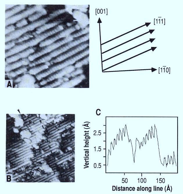
4 passing 1 µa of current for several minutes. The procedure had to b e repeated periodically to maintain tip resolution and stability. The dependence of the tunneling current on sample-tip separation was used to gauge the integrity of the vacuum gap. The standard vacuum tunneling equation was used to compute values of the effective barrier height between 4.2 and 5.0 ev (8). All of the images we present here were collected in the constant current mode at a 2.0 V sample bias with respect to the tip and a 0.1- na tunneling current and are presented after the subtraction of a background plane, which eliminates the tilt of the sample that would otherwise overwhelm small variations and make atomic features undetectable. Well-ordered areas were visible on the majority of the surface ( > 50 % when the tip was sharp), but observed less frequently after several days of analysis. Two of the observed structures are discussed below. Auger electron spectroscopy (AES) performed immediately after the initial thermal treatment and at the end of the STM analysis showed that the level of carbon contamination had increased, presumably through exposure to background gases in the vacuum chamber. Fourier analysis and direct measurement of the images in Fig. 2A and B indicates that the rows oriented in the [111] direction have an 8.5 Å periodicity and a 1 Å corrugation height. The corrugation directed along the rows has a 3.4 Å periodicity and a 0.2 Å amplitude. The width of these rows seems to vary somewhat and there are also numerous "missing cells.'' The bulk-terminated rutile lattice vectors have been added for comparison. The image in Fig. 2B shows a larger area containing two ledges o r atomic steps that are 2.2 Å in height, which is significantly less than the 4
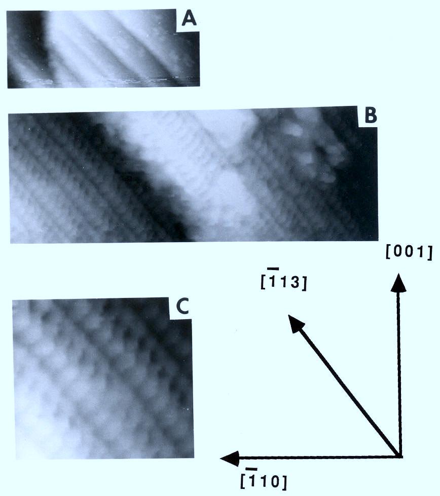
5 distance between adjacent (110) planes, which is 3.25 Å. Some regions of the image are either disordered or covered with adsorbates. Notice that the dark line that cuts across the image in Fig. 2B in the [113] direction (indicated by the arrow on the top left side of the image) a n d that forms a step edge in the lower portion of the picture. This feature is the same direction in which the rows and ledges found in Fig. 3, acquired from a different area of the crystal surface, are oriented. The largest rows in Fig. 3B, oriented in the [113] direction, are approximately 20 Å wide and are parallel to the large steps visible in Fig 3A. The height of the step in Fig. 3B is 9 Å. The detail in Fig 3C shows that each row is composed of discrete units arranged in a roughly hexagonal pattern. The structure shown in Fig. 2 differs from the one shown in Fig. 3, and neither can be explained by a simple surface termination of the bulk unit cell or some combination of unit cells. Two possible models can account for the observed surface structures, both of which rely on the presence of bulk nonstoichiometry. The geometries of both of the experimentally observed surface structures can be simply created by removing oxygen from the surface layer in the appropriate pattern; we call this the ordered-surface oxygen vacancy (OSOV) model. However, an STM image is not simply a reproduction of the surface geometry, but also depends on the surface density of states. Because all of the images were acquired at positive sample bias, electrons tunneled into unoccupied conduction band states that are predominantly Ti in origin. It follows that the light spots on the image reflect a greater density of Ti states, associated with the Ti atom positions, whereas the dark areas between the rows correspond to the absence of Ti states that occur at the O atom positions. This result 5
6 suggests that O must reside at the dark positions along the [111] a n d [113] directions while the other sites are vacant. However, at these positions, the tip is displaced downward by 1 Å, a rather large corrugation to arise from a change in the local density of states alone, especially considering that the presence of O atoms in these positions would presumably cause an additional opposite corrugation from purely geometric considerations. Because of this contradiction, the OSOV model does not seem plausible. The second model, the crystallographic shear (CS) model, avoids this contradiction by assuming that the major row corrugations are actually steps that would result naturally from CS displacements. The CS displacements can occur along a variety of planes including the (121) family of planes. The (121) plane intersects the (110) surface along t h e [111] direction, the same direction that the rows in Fig. 2 are oriented. The intersection of the (121) plane the (110) surface is in the direction [113], the same direction in which the rows in Fig. 3 are aligned. The CS displacement is always of the type 1 / 2 [011], which means that adjacent sections of the crystal are vertically displaced 1.6 Å with respect to one another along the line normal to the (110) surface. Because the plane subtraction applied to each image removes any global slope, a stepped structure appears saw-toothed, so that the intersection of each CS plane with the surface appears as a depression or dark spot on the image. The presence of excess Ti along the crystallographic shear planes should result in a corrugation which is opposite to the geometric effect. However, corrugations due to alterations in the electronic density of states are usually some tenths of angstroms, so this effect should not b e able to cancel the larger geometric effect. In fact, the observation that 6
7 the corrugations in Fig. 2 are about 1 Å, less than the expected value of 1.6 Å, suggests that the presence of excess Titanium in these positions compensates somewhat for the geometric effect. The disagreement between the expected and measured step height mentioned earlier m a y also be explained if each step is actually the sum of one (110) interplanar spacing and a CS plane. Although previous models of the reduced TiO 2 (110) surface have not considered the possible existence of CS planes or their effect on the titania surface structure (9), t h e existence of these planar defects has been proposed by Firment et al. (10) to explain angle-resolved UPS data from the reduced MoO 3 (010) surface, another transition metal oxide that forms a variety of CS structures. The spacing of the rows in Fig. 2 suggests that every sixth anion (121) plane is a CS plane and that the local composition in this area is Ti 3 O 5, while the spacing of the rows in Fig. 3 suggests that CS occurs a t every twelfth anion (121) plane and that the local composition is Ti 6 O 11. Although these phases are known to have a higher conductivity than rutile, they are still semiconducting, a fact verified by tunneling spectroscopy measurements. The 0.2 Å corrugations within the rows of Fig. 2 have a 3.4 Å spacing which is very close to the spacing of Ti atoms (3.5 Å) along this same direction in the ideal rutile unit cell. Apparently the nearest neighbor Ti atoms, separated by only 3 Å along the c axis, are not resolved. The distance between adjacent units within the rows of Fig. 3, measured parallel to the [110] direction, is approximately 6.4 Å, close to the bulk rutile unit cell spacing in that direction (6.5 Å). The distance between adjacent units in the [113] direction is 5.6 Å, which is the distance between the neighboring Ti atoms in that direction. 7
8 However, each Ti atom is clearly not imaged and a more detailed model for the atomic structure within the rows will have to be formed on the basis of additional experiments. 8
9 References and Notes 1. M. D. Kirk et al., Science 242, 1673 (1988); N. J. Zheng, U. Knipping, I. S. T. Tsong, W. T. Petuskey, J. C. Barry, J. Vac. Sci. Technol. A 6, 457 (1988); E. Garfunkel et al., Science 246, 99 (1989); X. L. Wu, Z. Zhang, Y. L. Wang, C. M. Lieber, ibid. 248,1211 (1990). 2. M. L. Norton, J. G. Mantovani, R. J. Warmack, J. Vac. Sci. Tech. A 7, 2898 (1989). 3. L. A. Bursill and B. G. Hyde, Prog. Solid State Chem. 7, 177 (1972). 4. S. E. Gilbert and J. E. Kennedy, J. Electrochem. Soc. 135, 2385 (1988); K. Itaya and E. Tomita, Chem. Lett., 285 (1985); K. Sakamaki, S. Matsunaga, K. Itoh, A. Fujishima, Y. Gohshi, Surf. Sci. 219, L531 (1989); S. E. GIlbert and J. H. Kennedy, Langmuir 5, 1412 (1989); Surf. Sci. 225, L1 (1990). 5. The 1.0 mm 5 mm 1.6 mm titania sample was oriented to within ± 1/2 of the (110) face by Laue diffraction and cut with a highspeed diamond saw from a single-crystal boule. The surface was polished by sequentially reducing the size of Al 2 O 3 grinding media down to 1 µ. The crystal was then reduced in UHV by annealing in a resistively heated tantalum boat at a temperature above 900 K (based upon color) for 36 hours. Following this treatment, the crystal was dark gray in color and opaque. The surface was then argon-ion milled for 5 min at 2 kv followed by 25 min of ion 9
10 bombardment at 500 V using an estimated current density of 5 to 10 µa/cm 2. The crystal was then annealed at 823 K for 30 min in 1 X 10⁻⁷ torr of oxygen in order to re-oxidize the surface and anneal out the damage produced by ion bombardment. 6. No ultraviolet photoelectron spectroscopy (UPS) data were taken on this surface, although the LEED patterns were similar to those on the TiO 2 (110) surfaces that exhibit no band gap defect surface states; see H. R. Sadeghi and V. E. Henrich, Appl. Surf. Sci. 19, 330 (1984). 7. The STM head was manufactured by WA technologies, Cambridge, England. 8. For details on the determination of the apparent barrier height, see J. K. Gimzewski and R. Moller, Phys. Rev. B 36, 1284 (1987); N. D. Lang, ibid, p. 8173; and G. Rohrer and D. Bonnell, J. Am. Ceram. Soc., in press. 9. W. Gopel, G. Rocker, R. Feierabend, Phys. Rev. B 28, 3427 (1983); V. Henrich, Rep. Prog. Phys. 48, 1481 (1985). 10 L. E. Firment, A. Ferretti, M. R. Cohen, R. P. Merrill, Langmuir 1, 166 (1985). 11. Supported at the University of Pennsylvania by IBM Research a n d the National Science Foundation and at Yale University by the National 10
11 Science Foundation solid state chemistry division grant DMR We thank Z. Zhang for assistance in preparing the sample surface. Fig. 1. Illustration of the CS plane formation process and the effect on the topography of the (110) surface. For simplicity, the structure is viewed parallel to the (100) direction in (A to C), while (D) is a perspective drawing that illustrates the effect of this operation on the (110) surface. (A) Idealized rutile structure; the larger circles represent O and small black circles represent Ti. (B) Oxygen vacancies formed along the (121) plane. (C) Translation of onehalf of the structure [the parts to the right of the (121) plane shown in (B)] by the vector 1/2[011] reestablishes the closepacked O framework and leaves the Ti atoms in antiphase positions. (D) The shear operations produce an ordered arrangement of steps on the (110) surface, as depicted in this perspective drawing. In this case, the steps are oriented in the [111] direction. Fig. 2. (A) An STM image showing a 109 Å by 109 Å area of the TiO 2 (110) surface. The vertical resolution from black to white is 2 Å, with lighter shades corresponding to topographic peaks. (B) A 246 Å by 246 Å area that includes several steps. The vertical resolution from black to white is 2.8 Å. (C) Profile taken along the line indicated in (B) shows the height of the steps. Fig. 3. (A) An STM image of a large terraced area (930 Å by 379 Å) with a series of steps oriented in the [113] direction. The vertical 11
12 resolution from black to white is 43 Å. (B) A more detailed scan (273 Å by 108 Å) of a region on the right side of (A). The vertical resolution from black to white is 9 Å. (C) An enlargement of a subsection of this image shows detail within each row. 12
13 [010] [001] (121) a) b) (121) [001] [111] (110) [100] [010] [110] (121) c) d)
14
15
The ability of the scanning tunneling microscope (STM) to record real-space, atomicscale
 to record real-space, atomicscale") EXPERIMENTAL AND SIMULATED SCANNING TUNNELING MICROSCOPY OF THE CLEAVED Rb 1 / 3 WO 3 (0001) SURFACE WEIER LU AND GREGORY S. ROHRER Carnegie Mellon University Department of Materials Science and Engineering
EXPERIMENTAL AND SIMULATED SCANNING TUNNELING MICROSCOPY OF THE CLEAVED Rb 1 / 3 WO 3 (0001) SURFACE WEIER LU AND GREGORY S. ROHRER Carnegie Mellon University Department of Materials Science and Engineering
IMAGING THE ATOMIC-SCALE STRUCTURE OF MOLYBDENUM AND VANADIUM OXIDES BY SCANNING TUNNELING MICROSCOPY
 IMAGING THE ATOMIC-SCALE STRUCTURE OF MOLYBDENUM AND VANADIUM OXIDES BY SCANNING TUNNELING MICROSCOPY GREGORY S. ROHRER, WEIER LU, AND RICHARD L. SMITH Carnegie Mellon University Department of Materials
Scanning Tunneling Microscopy Studies of the Ge(111) Surface
 Surface") VC Scanning Tunneling Microscopy Studies of the Ge(111) Surface Anna Rosen University of California, Berkeley Advisor: Dr. Shirley Chiang University of California, Davis August 24, 2007 Abstract: This
VC Scanning Tunneling Microscopy Studies of the Ge(111) Surface Anna Rosen University of California, Berkeley Advisor: Dr. Shirley Chiang University of California, Davis August 24, 2007 Abstract: This
Structure and apparent topography of TiO surfaces
 PHYSICAL REVIEW B VOLUME 56, NUMBER 16 Structure and apparent topography of TiO 2 110 surfaces 15 OCTOBER 1997-II Kwok-On Ng and David Vanderbilt Department of Physics and Astronomy, Rutgers University,
Surface Defects on Natural MoS 2
 Supporting Information: Surface Defects on Natural MoS 2 Rafik Addou 1*, Luigi Colombo 2, and Robert M. Wallace 1* 1 Department of Materials Science and Engineering, The University of Texas at Dallas,
SUPPLEMENTARY INFORMATION
 DOI: 10.1038/NCHEM.2491 Experimental Realization of Two-dimensional Boron Sheets Baojie Feng 1, Jin Zhang 1, Qing Zhong 1, Wenbin Li 1, Shuai Li 1, Hui Li 1, Peng Cheng 1, Sheng Meng 1,2, Lan Chen 1 and
2) Atom manipulation. Xe / Ni(110) Model: Experiment:
 Atom manipulation. Xe / Ni(110) Model: Experiment:") 2) Atom manipulation D. Eigler & E. Schweizer, Nature 344, 524 (1990) Xe / Ni(110) Model: Experiment: G.Meyer, et al. Applied Physics A 68, 125 (1999) First the tip is approached close to the adsorbate
2) Atom manipulation D. Eigler & E. Schweizer, Nature 344, 524 (1990) Xe / Ni(110) Model: Experiment: G.Meyer, et al. Applied Physics A 68, 125 (1999) First the tip is approached close to the adsorbate
STM spectroscopy (STS)
") STM spectroscopy (STS) di dv 4 e ( E ev, r) ( E ) M S F T F Basic concepts of STS. With the feedback circuit open the variation of the tunneling current due to the application of a small oscillating voltage
STM spectroscopy (STS) di dv 4 e ( E ev, r) ( E ) M S F T F Basic concepts of STS. With the feedback circuit open the variation of the tunneling current due to the application of a small oscillating voltage
Author(s) Okuyama, H; Aruga, T; Nishijima, M. Citation PHYSICAL REVIEW LETTERS (2003), 91(
 Okuyama, H; Aruga, T; Nishijima, M. Citation PHYSICAL REVIEW LETTERS (2003), 91(") Title Vibrational characterization of the Si(111)-(7x7) Author(s) Okuyama, H; Aruga, T; Nishijima, M Citation PHYSICAL REVIEW LETTERS (2003), 91( Issue Date 2003-12-19 URL http://hdl.handle.net/2433/49840
Title Vibrational characterization of the Si(111)-(7x7) Author(s) Okuyama, H; Aruga, T; Nishijima, M Citation PHYSICAL REVIEW LETTERS (2003), 91( Issue Date 2003-12-19 URL http://hdl.handle.net/2433/49840
Scanning tunneling microscopy studies of the TiO surface: Structure and the nucleation growth of Pd
 PHYSICAL REVIEW B VOLUME, NUMBER 20 15 NOVEMBER 1997-II Scanning tunneling microscopy studies of the TiO 2 110 surface: Structure and the nucleation growth of Pd C. Xu, X. Lai, G. W. Zajac,* and D. W.
Cross-Section Scanning Tunneling Microscopy of InAs/GaSb Superlattices
 Cross-Section Scanning Tunneling Microscopy of InAs/GaSb Superlattices Cecile Saguy A. Raanan, E. Alagem and R. Brener Solid State Institute. Technion, Israel Institute of Technology, Haifa 32000.Israel
Molecular Ordering at the Interface Between Liquid Water and Rutile TiO 2 (110)
") Molecular Ordering at the Interface Between Liquid Water and Rutile TiO 2 (110) B E A T R I C E B O N A N N I D i p a r t i m e n t o d i F i s i c a, U n i v e r s i t a di R o m a T o r V e r g a t a
Molecular Ordering at the Interface Between Liquid Water and Rutile TiO 2 (110) B E A T R I C E B O N A N N I D i p a r t i m e n t o d i F i s i c a, U n i v e r s i t a di R o m a T o r V e r g a t a
Surface Studies by Scanning Tunneling Microscopy
 Surface Studies by Scanning Tunneling Microscopy G. Binnig, H. Rohrer, Ch. Gerber, and E. Weibel IBM Zurich Research Laboratory, 8803 Ruschlikon-ZH, Switzerland (Received by Phys. Rev. Lett. on 30th April,
Supplementary information
 Supplementary information Supplementary Figure S1STM images of four GNBs and their corresponding STS spectra. a-d, STM images of four GNBs are shown in the left side. The experimental STS data with respective
Scanning Tunneling Microscopy. how does STM work? the quantum mechanical picture example of images how can we understand what we see?
 Scanning Tunneling Microscopy how does STM work? the quantum mechanical picture example of images how can we understand what we see? Observation of adatom diffusion with a field ion microscope Scanning
Low-temperature Scanning Tunneling Spectroscopy of Semiconductor Surfaces
 Low-temperature Scanning Tunneling Spectroscopy of Semiconductor Surfaces R. M. Feenstra 1 Department of Physics, Carnegie Mellon University, Pittsburgh, Pennsylvania 15213 G. Meyer 2 Paul Drude Institut
Molecular Dynamics on the Angstrom Scale
 Probing Interface Reactions by STM: Molecular Dynamics on the Angstrom Scale Zhisheng Li Prof. Richard Osgood Laboratory for Light-Surface Interactions, Columbia University Outline Motivation: Why do we
Observation of Bulk Defects by Scanning Tunneling Microscopy and Spectroscopy: Arsenic Antisite Defects in GaAs
 VOLUME 71, NUMBER 8 PH YSICAL REVI EW LETTERS 23 AUGUST 1993 Observation of Bulk Defects by Scanning Tunneling Microscopy and Spectroscopy: Arsenic Antisite Defects in GaAs R. M. Feenstra, J. M. Woodall,
Crystalline Surfaces for Laser Metrology
 Crystalline Surfaces for Laser Metrology A.V. Latyshev, Institute of Semiconductor Physics SB RAS, Novosibirsk, Russia Abstract: The number of methodological recommendations has been pronounced to describe
Supporting Online Material for
 www.sciencemag.org/cgi/content/full/315/5819/1692/dc1 Supporting Online Material for Enhanced Bonding of Gold Nanoparticles on Oxidized TiO 2 (110) D. Matthey, J. G. Wang, S. Wendt, J. Matthiesen, R. Schaub,
Special Properties of Au Nanoparticles
 Special Properties of Au Nanoparticles Maryam Ebrahimi Chem 7500/750 March 28 th, 2007 1 Outline Introduction The importance of unexpected electronic, geometric, and chemical properties of nanoparticles
Reduced preferential sputtering of TiO 2 (and Ta 2 O 5 ) thin films through argon cluster ion bombardment.
 thin films through argon cluster ion bombardment.") NATIOMEM Reduced preferential sputtering of TiO 2 (and Ta 2 O 5 ) thin films through argon cluster ion bombardment. R. Grilli *, P. Mack, M.A. Baker * * University of Surrey, UK ThermoFisher Scientific
NATIOMEM Reduced preferential sputtering of TiO 2 (and Ta 2 O 5 ) thin films through argon cluster ion bombardment. R. Grilli *, P. Mack, M.A. Baker * * University of Surrey, UK ThermoFisher Scientific
SUPPLEMENTARY INFORMATION
 In the format provided by the authors and unedited. Intrinsically patterned two-dimensional materials for selective adsorption of molecules and nanoclusters X. Lin 1,, J. C. Lu 1,, Y. Shao 1,, Y. Y. Zhang
Supporting Information
 Supporting Information Spatially-resolved imaging on photocarrier generations and band alignments at perovskite/pbi2 hetero-interfaces of perovskite solar cells by light-modulated scanning tunneling microscopy
Direct observation of a Ga adlayer on a GaN(0001) surface by LEED Patterson inversion. Xu, SH; Wu, H; Dai, XQ; Lau, WP; Zheng, LX; Xie, MH; Tong, SY
 surface by LEED Patterson inversion. Xu, SH; Wu, H; Dai, XQ; Lau, WP; Zheng, LX; Xie, MH; Tong, SY") Title Direct observation of a Ga adlayer on a GaN(0001) surface by LEED Patterson inversion Author(s) Xu, SH; Wu, H; Dai, XQ; Lau, WP; Zheng, LX; Xie, MH; Tong, SY Citation Physical Review B - Condensed
Title Direct observation of a Ga adlayer on a GaN(0001) surface by LEED Patterson inversion Author(s) Xu, SH; Wu, H; Dai, XQ; Lau, WP; Zheng, LX; Xie, MH; Tong, SY Citation Physical Review B - Condensed
Tunneling spectroscopic analysis of optically active wide band.. gap semiconductors
 Tunneling spectroscopic analysis of optically active wide band.. gap semiconductors D. A Bonnell and G. S. Rohrer") The University of Pennsylvania, Philadelphia, Pennsylvania 19104 R. H. French E. 1. DuPont
Oxygen-induced p(3 1) reconstruction of the W(100) surface
 reconstruction of the W(100) surface") Oxygen-induced p(3 1) reconstruction of the W(100) surface S. Murphy 1, G. Manai, I.V. Shvets SFI Laboratory, Physics Department, Trinity College, Dublin 2, Ireland Abstract The oxidation of the W(100)
Oxygen-induced p(3 1) reconstruction of the W(100) surface S. Murphy 1, G. Manai, I.V. Shvets SFI Laboratory, Physics Department, Trinity College, Dublin 2, Ireland Abstract The oxidation of the W(100)
Chapter 2 Surface Science Studies of Metal Oxide Gas Sensing Materials
 Chapter 2 Surface Science Studies of Metal Oxide Gas Sensing Materials Junguang Tao and Matthias Batzill Abstract In this chapter we present recent advances in the study of metal oxide surfaces and put
Direct Observation of Nodes and Twofold Symmetry in FeSe Superconductor
 www.sciencemag.org/cgi/content/full/332/6036/1410/dc1 Supporting Online Material for Direct Observation of Nodes and Twofold Symmetry in FeSe Superconductor Can-Li Song, Yi-Lin Wang, Peng Cheng, Ye-Ping
Electronic States of Oxidized GaN(0001) Surfaces
 Surfaces") Electronic States of Oxidized GaN(0001) Surfaces Y. Dong and R. M. Feenstra Dept. Physics, Carnegie Mellon University, Pittsburgh, PA 15213 J. E. Northrup Palo Alto Research Center, 3333 Coyote Hill Road,
Electronic States of Oxidized GaN(0001) Surfaces Y. Dong and R. M. Feenstra Dept. Physics, Carnegie Mellon University, Pittsburgh, PA 15213 J. E. Northrup Palo Alto Research Center, 3333 Coyote Hill Road,
Application of single crystalline tungsten for fabrication of high resolution STM probes with controlled structure 1
 Application of single crystalline tungsten for fabrication of high resolution STM probes with controlled structure 1 A. N. Chaika a, S. S. Nazin a, V. N. Semenov a, V. G. Glebovskiy a, S. I. Bozhko a,b,
Scanning Tunneling Microscopy
 Scanning Tunneling Microscopy References: 1. G. Binnig, H. Rohrer, C. Gerber, and Weibel, Phys. Rev. Lett. 49, 57 (1982); and ibid 50, 120 (1983). 2. J. Chen, Introduction to Scanning Tunneling Microscopy,
THE ATOMIC-SCALE CHARACTERIZATION OF DEFECTS ON CLEAVED VANADIUM AND MOLYBDENUM OXIDE SURFACES USING STM
 THE ATOMIC-SCALE CHARACTERIZATION OF DEFECTS ON CLEAVED VANADIUM AND MOLYBDENUM OXIDE SURFACES USING STM GREGORY S. ROHRER AND RICHARD L. SMITH Carnegie Mellon University Department of Materials Science
Indium incorporation and surface segregation during InGaN growth by molecular beam epitaxy: experiment and theory
 Indium incorporation and surface segregation during InGaN growth by molecular beam epitaxy: experiment and theory Huajie Chen 1,1 R. M. Feenstra 1, J. E. Northrup 2, J. Neugebauer 3, and D. W. Greve 4
8 Summary and outlook
 91 8 Summary and outlook The main task of present work was to investigate the growth, the atomic and the electronic structures of Co oxide as well as Mn oxide films on Ag(001) by means of STM/STS at LT
Supplementary Figure 1 Experimental setup for crystal growth. Schematic drawing of the experimental setup for C 8 -BTBT crystal growth.
 Supplementary Figure 1 Experimental setup for crystal growth. Schematic drawing of the experimental setup for C 8 -BTBT crystal growth. Supplementary Figure 2 AFM study of the C 8 -BTBT crystal growth
Surface of Sputtered and Annealed Polar SrTiO 3 (111): TiO x -Rich (n n) Reconstructions
: TiO x -Rich (n n) Reconstructions") 6538 J. Phys. Chem. C 2008, 112, 6538-6545 Surface of Sputtered and Annealed Polar SrTiO 3 (111): TiO x -Rich (n n) Reconstructions Bruce C. Russell and Martin R. Castell* Department of Materials, UniVersity
6538 J. Phys. Chem. C 2008, 112, 6538-6545 Surface of Sputtered and Annealed Polar SrTiO 3 (111): TiO x -Rich (n n) Reconstructions Bruce C. Russell and Martin R. Castell* Department of Materials, UniVersity
A high-pressure-induced dense CO overlayer on Pt(111) surface: A chemical analysis using in-situ near ambient pressure XPS
 surface: A chemical analysis using in-situ near ambient pressure XPS") Electronic Supplementary Material (ESI) for Physical Chemistry Chemical Physics. This journal is the Owner Societies 2014 Electronic Supplementary Information for A high-pressure-induced dense CO overlayer
Electronic Supplementary Material (ESI) for Physical Chemistry Chemical Physics. This journal is the Owner Societies 2014 Electronic Supplementary Information for A high-pressure-induced dense CO overlayer
Experimental methods in physics. Local probe microscopies I
 Experimental methods in physics Local probe microscopies I Scanning tunnelling microscopy (STM) Jean-Marc Bonard Academic year 09-10 1. Scanning Tunneling Microscopy 1.1. Introduction Image of surface
M2 TP. Low-Energy Electron Diffraction (LEED)
") M2 TP Low-Energy Electron Diffraction (LEED) Guide for report preparation I. Introduction: Elastic scattering or diffraction of electrons is the standard technique in surface science for obtaining structural
M2 TP Low-Energy Electron Diffraction (LEED) Guide for report preparation I. Introduction: Elastic scattering or diffraction of electrons is the standard technique in surface science for obtaining structural
Cross-sectional scanning tunneling microscopy of InAsSb/InAsP superlattices
 Cross-sectional scanning tunneling microscopy of InAsSb/InAsP superlattices S. L. Zuo and E. T. Yu a) Department of Electrical and Computer Engineering, University of California at San Diego, La Jolla,
S: spin quantum number
 substance: titanium oxide (TiO 2 ) property: ESR parameters of native defects in pure n-type TiO 2 x (rutile) e CB S principal g-value e CB : number of conduction band electrons axes per defect S: spin
Supplementary Information:
 Supplementary Figures Supplementary Information: a b 1 2 3 0 ΔZ (pm) 66 Supplementary Figure 1. Xe adsorbed on a Cu(111) surface. (a) Scanning tunnelling microscopy (STM) topography of Xe layer adsorbed
NTEGRA for EC PRESENTATION
 NTEGRA for EC PRESENTATION Application Purpose: In-situ control/modification of the surface morphology of single crystal and polycrystal electrodes (samples) during electrochemical process (in situ) in
Surface structure vs. surface science; Atomic imaging of surface with STM; Nanoscale surface probing with STM; Exploration of surface catalysis.
 Lecture 7: STM Atomic Imaging of Metal and Semiconductor Surface Surface structure vs. surface science; Atomic imaging of surface with STM; Nanoscale surface probing with STM; Exploration of surface catalysis.
Reflection high energy electron diffraction and scanning tunneling microscopy study of InP(001) surface reconstructions
 surface reconstructions") Reflection high energy electron diffraction and scanning tunneling microscopy study of InP(001) surface reconstructions V.P. LaBella, Z. Ding, D.W. Bullock, C. Emery, and P.M. Thibado Department of Physics,
Reflection high energy electron diffraction and scanning tunneling microscopy study of InP(001) surface reconstructions V.P. LaBella, Z. Ding, D.W. Bullock, C. Emery, and P.M. Thibado Department of Physics,
C. D. Lee and R. M. Feenstra Dept. Physics, Carnegie Mellon University, Pittsburgh, PA 15213
 Morphology and surface reconstructions of GaN(1 1 00) surfaces C. D. Lee and R. M. Feenstra Dept. Physics, Carnegie Mellon University, Pittsburgh, PA 15213 J. E. Northrup Palo Alto Research Center, 3333
REPORT ON SCANNING TUNNELING MICROSCOPE. Course ME-228 Materials and Structural Property Correlations Course Instructor Prof. M. S.
 REPORT ON SCANNING TUNNELING MICROSCOPE Course ME-228 Materials and Structural Property Correlations Course Instructor Prof. M. S. Bobji Submitted by Ankush Kumar Jaiswal (09371) Abhay Nandan (09301) Sunil
Imaging Methods: Scanning Force Microscopy (SFM / AFM)
") Imaging Methods: Scanning Force Microscopy (SFM / AFM) The atomic force microscope (AFM) probes the surface of a sample with a sharp tip, a couple of microns long and often less than 100 Å in diameter.
Imaging Methods: Scanning Force Microscopy (SFM / AFM) The atomic force microscope (AFM) probes the surface of a sample with a sharp tip, a couple of microns long and often less than 100 Å in diameter.
CHAPTER 5 ATOMIC HYDROGEN
 CHAPTER 5 TEMPERATURE DEPENDENT ETCHING OF THE DIAMOND (100) SURFACE BY ATOMIC HYDROGEN 5.1 Introduction Described in previous chapters of this dissertation are the results of the initial UHV STM studies
Scanning Probe Microscopy
 1 Scanning Probe Microscopy Dr. Benjamin Dwir Laboratory of Physics of Nanostructures (LPN) Benjamin.dwir@epfl.ch PH.D3.344 Outline: Introduction: What is SPM, history STM AFM Image treatment Advanced
Intrinsic vacancy induced nanoscale wire structure in heteroepitaxial Ga 2 Se 3 /Si(001)
") Intrinsic vacancy induced nanoscale wire structure in heteroepitaxial Ga 2 Se 3 /Si(001) Taisuke Ohta, 1, D. A. Schmidt, 2 Shuang Meng, 2, A. Klust, 2, A. Bostwick, 2, Q. Yu, 2 Marjorie A. Olmstead, 2
Intrinsic vacancy induced nanoscale wire structure in heteroepitaxial Ga 2 Se 3 /Si(001) Taisuke Ohta, 1, D. A. Schmidt, 2 Shuang Meng, 2, A. Klust, 2, A. Bostwick, 2, Q. Yu, 2 Marjorie A. Olmstead, 2
3.1 Electron tunneling theory
 Scanning Tunneling Microscope (STM) was invented in the 80s by two physicists: G. Binnig and H. Rorher. They got the Nobel Prize a few years later. This invention paved the way for new possibilities in
Mater. Res. Soc. Symp. Proc. Vol Materials Research Society
 Mater. Res. Soc. Symp. Proc. Vol. 1217 2010 Materials Research Society 1217-Y08-43 Surface Structure of Pd 3 Fe(111) and Effects of Oxygen Adsorption Xiaofang Yang, Lindsey A. Welch, Jie Fu and Bruce E.
A constant potential of 0.4 V was maintained between electrodes 5 and 6 (the electrode
 (a) (b) Supplementary Figure 1 The effect of changing po 2 on the field-enhanced conductance A constant potential of 0.4 V was maintained between electrodes 5 and 6 (the electrode configuration is shown
b imaging by a double tip potential
 Supplementary Figure Measurement of the sheet conductance. Resistance as a function of probe spacing including D and 3D fits. The distance is plotted on a logarithmic scale. The inset shows corresponding
Properties of Individual Nanoparticles
 TIGP Introduction technology (I) October 15, 2007 Properties of Individual Nanoparticles Clusters 1. Very small -- difficult to image individual nanoparticles. 2. New physical and/or chemical properties
Hydrogen termination following Cu deposition on Si(001)
") Hydrogen termination following Cu deposition on Si(001) L. A. Baker, A. R. Laracuente,* and L. J. Whitman Naval Research Laboratory, Washington, DC 20375-5342, USA Received 9 September 2004; published
Hydrogen termination following Cu deposition on Si(001) L. A. Baker, A. R. Laracuente,* and L. J. Whitman Naval Research Laboratory, Washington, DC 20375-5342, USA Received 9 September 2004; published
Energy level alignment and two-dimensional structure of pentacene on Au 111 surfaces
 JOURNAL OF APPLIED PHYSICS VOLUME 91, NUMBER 5 1 MARCH 2002 Energy level alignment and two-dimensional structure of pentacene on Au 111 surfaces P. G. Schroeder, C. B. France, J. B. Park, and B. A. Parkinson
Scanning Tunneling Microscopy
 Scanning Tunneling Microscopy A scanning tunneling microscope (STM) is an instrument for imaging surfaces at the atomic level. Its development in 1981 earned its inventors, Gerd Binnig and Heinrich Rohrer
Microscopical and Microanalytical Methods (NANO3)
") Microscopical and Microanalytical Methods (NANO3) 06.11.15 10:15-12:00 Introduction - SPM methods 13.11.15 10:15-12:00 STM 20.11.15 10:15-12:00 STS Erik Zupanič erik.zupanic@ijs.si stm.ijs.si 27.11.15
Microscopical and Microanalytical Methods (NANO3) 06.11.15 10:15-12:00 Introduction - SPM methods 13.11.15 10:15-12:00 STM 20.11.15 10:15-12:00 STS Erik Zupanič erik.zupanic@ijs.si stm.ijs.si 27.11.15
General concept and defining characteristics of AFM. Dina Kudasheva Advisor: Prof. Mary K. Cowman
 General concept and defining characteristics of AFM Dina Kudasheva Advisor: Prof. Mary K. Cowman Overview Introduction History of the SPM invention Technical Capabilities Principles of operation Examples
M. Enachescu Materials Sciences Division, Lawrence Berkeley National Laboratory, University of California, Berkeley, California 94720
 JOURNAL OF APPLIED PHYSICS VOLUME 95, NUMBER 12 15 JUNE 2004 The role of contaminants in the variation of adhesion, friction, and electrical conduction properties of carbide-coated scanning probe tips
Excitations and Interactions
 Excitations and Interactions Magnon gases A7 A8 Spin physics A3 A5 A9 A10 A12 Quantum magnets A3 A8 B1 B2 B3 B4 B5 Synthesis B4 B6 B10 E Spectroscopy B11 Excitations and Interactions Charge-transfer induced
Scanning Tunneling Microscopy
 Scanning Tunneling Microscopy References: 1. G. Binnig, H. Rohrer, C. Gerber, and Weibel, Phys. Rev. Lett. 49, 57 (1982); and ibid 50, 120 (1983). 2. J. Chen, Introduction to Scanning Tunneling Microscopy,
tip of a current tip and the sample. Components: 3. Coarse sample-to-tip isolation system, and
 SCANNING TUNNELING MICROSCOPE Brief history: Heinrich Rohrer and Gerd K. Binnig, scientists at IBM's Zurich Research Laboratory in Switzerland, are awarded the 1986 Nobel Prize in physicss for their work
Characterization of metal clusters (Pd and Au) supported on various metal oxide surfaces (MgO and TiO 2 )
 supported on various metal oxide surfaces (MgO and TiO 2 )") Characterization of metal clusters (Pd and Au) supported on various metal oxide surfaces (MgO and TiO 2 ) C. Xu, W. S. Oh, G. Liu, D. Y. Kim, a) and D. W. Goodman b) Department of Chemistry, Texas A&M
Characterization of metal clusters (Pd and Au) supported on various metal oxide surfaces (MgO and TiO 2 ) C. Xu, W. S. Oh, G. Liu, D. Y. Kim, a) and D. W. Goodman b) Department of Chemistry, Texas A&M
Lecture 12. study surfaces.
 Lecture 12 Solid Surfaces Techniques to Solid Surfaces. Techniques to study surfaces. Solid Surfaces Molecules on surfaces are not mobile (to large extent) Surfaces have a long-range order (crystalline)
672 Advanced Solid State Physics. Scanning Tunneling Microscopy
 672 Advanced Solid State Physics Scanning Tunneling Microscopy Biao Hu Outline: 1. Introduction to STM 2. STM principle & working modes 3. STM application & extension 4. STM in our group 1. Introduction
From manipulation of the charge state to imaging of individual molecular orbitals and bond formation
 Scanning Probe Microscopy of Adsorbates on Insulating Films: From manipulation of the charge state to imaging of individual molecular orbitals and bond formation Gerhard Meyer, Jascha Repp, Peter Liljeroth
Metal Oxides Surfaces
 Chapter 2 Metal xides Surfaces 2.1 Cobalt xides 1. Co Co (cobalt monoxide) with rocksalt structure (NaCl structure) consists of two interpenetrating fcc sublattices of Co 2+ and 2. These two sublattices
Self-Assembly of Two-Dimensional Organic Networks Containing Heavy Metals (Pb, Bi) and Preparation of Spin-Polarized Scanning Tunneling Microscope
 and Preparation of Spin-Polarized Scanning Tunneling Microscope") MPhil Thesis Defense Self-Assembly of Two-Dimensional Organic Networks Containing Heavy Metals (Pb, Bi) and Preparation of Spin-Polarized Scanning Tunneling Microscope Presented by CHEN Cheng 12 th Aug.
MPhil Thesis Defense Self-Assembly of Two-Dimensional Organic Networks Containing Heavy Metals (Pb, Bi) and Preparation of Spin-Polarized Scanning Tunneling Microscope Presented by CHEN Cheng 12 th Aug.
Surface Structure and Lattice Vibrations of MnO(001) Analyzed by High-resolution Medium Energy Ion Scattering Spectroscopy
 Analyzed by High-resolution Medium Energy Ion Scattering Spectroscopy") Surface Structure and Lattice Vibrations of MnO(001) Analyzed by High-resolution Medium Energy Ion Scattering Spectroscopy Tetsuaki Okazawa and Yoshiaki Kido Abstract Clean MnO(001)-1 1 surfaces were successfully
Surface Structure and Lattice Vibrations of MnO(001) Analyzed by High-resolution Medium Energy Ion Scattering Spectroscopy Tetsuaki Okazawa and Yoshiaki Kido Abstract Clean MnO(001)-1 1 surfaces were successfully
Initial growth of Au on oxides
 SURFACE AND INTERFACE ANALYSIS Surf. Interface Anal. 2001; 32: 161 165 Initial growth of Au on oxides Qinlin Guo, 1 Kai Luo, 2 Kent A. Davis 2 and D. W. Goodman 2 1 State Key Laboratory for Surface Physics,
Introduction to Scanning Tunneling Microscopy
 Introduction to Scanning Tunneling Microscopy C. JULIAN CHEN IBM Research Division Thomas J. Watson Research Center Yorktown Heights, New York New York Oxford OXFORD UNIVERSITY PRESS 1993 CONTENTS List
Scanning tunneling microscopy
 IFM The Department of Physics, Chemistry and Biology Lab 72 in TFFM08 Scanning tunneling microscopy NAME PERS. - NUMBER DATE APPROVED Rev. Dec 2006 Ivy Razado Aug 2014 Tuomas Hänninen Contents 1 Introduction
High resolution STM imaging with oriented single crystalline tips
 High resolution STM imaging with oriented single crystalline tips A. N. Chaika a, *, S. S. Nazin a, V. N. Semenov a, N. N Orlova a, S. I. Bozhko a,b, O. Lübben b, S. A. Krasnikov b, K. Radican b, and I.
Breakdown of cation vacancies into anion vacancy-antisite complexes on III-V semiconductor surfaces
 Breakdown of cation vacancies into anion vacancy-antisite complexes on III-V semiconductor surfaces A. Höglund and S. Mirbt Department of Physics, Uppsala University, Box 530, SE-75121 Uppsala, Sweden
Scanning Tunneling Microscopy/Spectroscopy on Superconducting Diamond Films
 T. New Nishizaki Diamond et and al. Frontier Carbon Technology 21 Vol. 17, No. 1 2007 MYU Tokyo NDFCT 530 Scanning Tunneling Microscopy/Spectroscopy on Superconducting Diamond Films Terukazu Nishizaki
Instrumentation and Operation
 Instrumentation and Operation 1 STM Instrumentation COMPONENTS sharp metal tip scanning system and control electronics feedback electronics (keeps tunneling current constant) image processing system data
Solid Surfaces, Interfaces and Thin Films
 Hans Lüth Solid Surfaces, Interfaces and Thin Films Fifth Edition With 427 Figures.2e Springer Contents 1 Surface and Interface Physics: Its Definition and Importance... 1 Panel I: Ultrahigh Vacuum (UHV)
Supporting Information. Surface-Enhanced Polymerization via Schiff-base Coupling. at the Solid-Water Interface under ph-control. and Claudio Goletti d
 Supporting Information Surface-Enhanced Polymerization via Schiff-base Coupling at the Solid-Water Interface under ph-control Marco Di Giovannantonio, a,b Tomasz Kosmala, a,c Beatrice Bonanni, d Giulia
Scanning Probe Microscopy. EMSE-515 F. Ernst
 Scanning Probe Microscopy EMSE-515 F. Ernst 1 Literature 2 3 Scanning Probe Microscopy: The Lab on a Tip by Ernst Meyer,Ans Josef Hug,Roland Bennewitz 4 Scanning Probe Microscopy and Spectroscopy : Theory,
Hydrogen-Induced Changes in Palladium Surface Structure: Field Ion Microscopy Study
 Vol. 114 (2008) ACTA PHYSICA POLONICA A Supplement Proceedings of the Professor Stefan Mróz Symposium Hydrogen-Induced Changes in Palladium Surface Structure: Field Ion Microscopy Study A. Tomaszewska
Spectro-microscopic photoemission evidence of surface dissociation and charge uncompensated areas in Pb(Zr,Ti)O 3 (001) layers
O 3 (001) layers") Electronic Supplementary Material (ESI) for Physical Chemistry Chemical Physics. This journal is the Owner Societies 2014 Electronic Supplementary Information - Phys. Chem. Chem. Phys. Spectro-microscopic
Electronic Supplementary Material (ESI) for Physical Chemistry Chemical Physics. This journal is the Owner Societies 2014 Electronic Supplementary Information - Phys. Chem. Chem. Phys. Spectro-microscopic
INTRODUCTION TO SCA\ \I\G TUNNELING MICROSCOPY
 INTRODUCTION TO SCA\ \I\G TUNNELING MICROSCOPY SECOND EDITION C. JULIAN CHEN Department of Applied Physics and Applied Mathematics, Columbia University, New York OXFORD UNIVERSITY PRESS Contents Preface
Role of Si adatoms in the Si 111 -Au 5 2 quasi-one-dimensional system
 PHYSICAL REVIEW B VOLUME 55, NUMBER 23 15 JUNE 1997-I Role of Si adatoms in the Si 111 -Au 5 2 quasi-one-dimensional system I. G. Hill and A. B. McLean Department of Physics, Queen s University, Kingston,
Formation of Halogen Bond-Based 2D Supramolecular Assemblies by Electric Manipulation
 Formation of Halogen Bond-Based 2D Supramolecular Assemblies by Electric Manipulation Qing-Na Zheng, a,b Xuan-He Liu, a,b Ting Chen, a Hui-Juan Yan, a Timothy Cook, c Dong Wang* a, Peter J. Stang, c Li-Jun
Interaction of Hydrogen on a Lanthanum hexaboride (111) Surface Jenna Cameli, Aashani Tillekaratne, Michael Trenary Department of Chemistry,
 Surface Jenna Cameli, Aashani Tillekaratne, Michael Trenary Department of Chemistry,") Interaction of Hydrogen on a Lanthanum hexaboride (111) Surface Jenna Cameli, Aashani Tillekaratne, Michael Trenary Department of Chemistry, University of Illinois at Chicago, Chicago, IL 60607 1 Abstract
Interaction of Hydrogen on a Lanthanum hexaboride (111) Surface Jenna Cameli, Aashani Tillekaratne, Michael Trenary Department of Chemistry, University of Illinois at Chicago, Chicago, IL 60607 1 Abstract
SUPPLEMENTARY NOTES Supplementary Note 1: Fabrication of Scanning Thermal Microscopy Probes
 SUPPLEMENTARY NOTES Supplementary Note 1: Fabrication of Scanning Thermal Microscopy Probes Fabrication of the scanning thermal microscopy (SThM) probes is summarized in Supplementary Fig. 1 and proceeds
Chapter 10. Nanometrology. Oxford University Press All rights reserved.
 Chapter 10 Nanometrology Oxford University Press 2013. All rights reserved. 1 Introduction Nanometrology is the science of measurement at the nanoscale level. Figure illustrates where nanoscale stands
Structure And Surface Alloying of Sn on a Pt(110) Single Crystal
 Single Crystal") Lehigh University Lehigh Preserve Theses and Dissertations 2011 Structure And Surface Alloying of Sn on a Pt(110) Single Crystal Jie Fu Lehigh University Follow this and additional works at: http://preserve.lehigh.edu/etd
Lehigh University Lehigh Preserve Theses and Dissertations 2011 Structure And Surface Alloying of Sn on a Pt(110) Single Crystal Jie Fu Lehigh University Follow this and additional works at: http://preserve.lehigh.edu/etd
" which has been adapted to a stainless-steel glove
 PHYSICAL REVIEW B VOLUME 42, NUMBER 3 15 JULY 1990-II Rapid Communications Rapid Communications are intended for the accelerated publication of important new results and are therefore given priority treatment
Two-dimensional lattice
 Two-dimensional lattice a 1 *, k x k x =0,k y =0 X M a 2, y Γ X a 2 *, k y a 1, x Reciprocal lattice Γ k x = 0.5 a 1 *, k y =0 k x = 0, k y = 0.5 a 2 * k x =0.5a 1 *, k y =0.5a 2 * X X M k x = 0.25 a 1
Vacancy migration, adatom motion, a.nd atomic bistability on the GaAs(110) surface studied by scanning tunneling microscopy
 surface studied by scanning tunneling microscopy") acancy migration, adatom motion, a.nd atomic bistability on the GaAs(110) surface studied by scanning tunneling microscopy s. Gwo, A. R. Smith, and C. K. Shih Department of Physics, The University of Texas
acancy migration, adatom motion, a.nd atomic bistability on the GaAs(110) surface studied by scanning tunneling microscopy s. Gwo, A. R. Smith, and C. K. Shih Department of Physics, The University of Texas
MSE 321 Structural Characterization
 Auger Spectroscopy Auger Electron Spectroscopy (AES) Scanning Auger Microscopy (SAM) Incident Electron Ejected Electron Auger Electron Initial State Intermediate State Final State Physical Electronics
Surface Sensitivity & Surface Specificity
 Surface Sensitivity & Surface Specificity The problems of sensitivity and detection limits are common to all forms of spectroscopy. In its simplest form, the question of sensitivity boils down to whether
ELECTRON CURRENT IMAGE DIFFRACTION FROM CRYSTAL SURFACES AT LOW ENERGIES
 C. BRENT BARGERON, A. NORMAN JETTE, and BERRY H. NALL ELECTRON CURRENT IMAGE DIFFRACTION FROM CRYSTAL SURFACES AT LOW ENERGIES Low-energy electron diffraction patterns in current images of crystal surfaces
Enantiospecific Desorption of Chiral Compounds from Chiral Cu(643) and Achiral Cu(111) Surfaces
 and Achiral Cu(111) Surfaces") Published on Web 02/13/2002 Enantiospecific Desorption of Chiral Compounds from Chiral Cu(643) and Achiral Cu(111) Surfaces Joshua D. Horvath and Andrew J. Gellman* Contribution from the Department of
Published on Web 02/13/2002 Enantiospecific Desorption of Chiral Compounds from Chiral Cu(643) and Achiral Cu(111) Surfaces Joshua D. Horvath and Andrew J. Gellman* Contribution from the Department of
Energy Spectroscopy. Ex.: Fe/MgO
 Energy Spectroscopy Spectroscopy gives access to the electronic properties (and thus chemistry, magnetism,..) of the investigated system with thickness dependence Ex.: Fe/MgO Fe O Mg Control of the oxidation