Surface structure vs. surface science; Atomic imaging of surface with STM; Nanoscale surface probing with STM; Exploration of surface catalysis.
|
|
|
- Godfrey Clement Morton
- 6 years ago
- Views:
Transcription
1 Lecture 7: STM Atomic Imaging of Metal and Semiconductor Surface Surface structure vs. surface science; Atomic imaging of surface with STM; Nanoscale surface probing with STM; Exploration of surface catalysis.
2 Surface Science The Nobel Prize in Chemistry 2007 "for his studies of chemical processes on solid surfaces" Gerhard Ertl Germany Fritz-Haber-Institut der Max-Planck- Gesellschaft Berlin, Germany b. 1936
3 Description of crystalline surface: Terrace Step Kink (TSK) model TSK model, also referred to as Terrace Ledge Kink (TLK) model, describes the thermodynamics of crystal surface formation and transformation, as well as the energetics of surface defect formation. The TSK model can be applied successfully to surface science topics such as crystal growth (including epitaxial growth), surface diffusion, roughening, and vaporization, because it consider the two major points about the surface: 1. The energy of an atom s position on a crystal surface is determined by its bonding to neighboring atoms; 2. Phase growth or transition simply involve the counting of broken and formed bonds. The TSK model was originally proposed by Kossel and Stranski. Terrace Island

4 A place in Egypt, or Middle East? A Copper Surface This is what a copper surface looks like through the STM
5 What is Surface? Surface --- the boundary layer between a solid and a vacuum, gas, or liquid. Occasionally surface also refers to the boundary between liquid and gas phase. Surface differs substantially from the interior of the solid both in chemical composition and physical properties (what differences?): unsaturated atoms for binding or adsorption, more exposure to air or liquid, more? As the dimension of a solid becomes smaller (in nanometer range), the ratio of surface atoms increases dramatically (draw scheme on board: 4 atoms cube). For a 3 nm CdSe nanoparticle, ~ 50% atoms are on surface, while for a large bulk material, the surface layer is generally only a tiny fraction of the total solid.
6 Surface Science Surface science is the study of physical and chemical phenomena that occur at the surfaces. Surface science includes the fields of surface chemistry and surface physics, though some related practical applications are classed as surface engineering. Surface science covers the concepts such as 1. heterogeneous catalysis, see slides 2. semiconductor devices (p-n junctions, interfacial CT), see slides 3. fuel cells, see slides 4. self-assembled monolayers, see slides 5. corrosion and adhesion, 6. metal/alloy surface, 7. behavior and function of biological membranes.
7 Surface Chemistry Surface chemistry can be roughly defined as the study of chemical reactions at interfaces, aiming at modifying the chemical composition of a surface by incorporation of selected elements or functional groups that produce various desired effects or improvements in the properties of the surface or interface. Surface chemistry is of particular importance to the field of heterogeneous catalysis. Particularly, the adhesion of gas or liquid molecules to the surface is known as adsorption. Although this can be due to either chemisorption or by physisorption, these two are included in surface chemistry. The field of surface chemistry started with heterogeneous catalysis pioneered by Paul Sabatier on hydrogenation and Fritz Haber on the Haber process. Irving Langmuir was also one of the founders of this field, and the Langmuir adsorption equation is used to model monolayer adsorption where all surface adsorption sites have the same affinity for the adsorbing species. Most recent developments in surface sciences include the 2007 Nobel Prize of Chemistry winner Gerhard Ertl's advancements in surface chemistry, specifically his investigation of the interaction between carbon monoxide molecules and platinum and other catalysts surfaces, as well as their catalytic conversion into carbon dioxides.
8 Surface Physics Surface physics can be roughly defined as the study of physical changes that occur at interfaces. Some of the things investigated by surface physics include surface states, surface diffusion, surface reconstruction, surface phonons and plasmons, epitaxy and surface enhanced Raman scattering, the emission and tunneling of electrons, spintronics, and the self-assembly of nanostructures on surface. Very often, Surface physics overlaps with surface chemistry, particularly at the very ultimate atomic or molecular scale, where physics and chemistry are no longer distinct by the traditional definition. As traditionally defined, a physical change in a substance doesn't change what the substance is. In a chemical change where there is a chemical reaction, a new substance is formed and energy is either given off or absorbed. For example, if a piece of paper is cut up into small pieces it still is paper. This would be a physical change in the shape and size of the paper. If the same piece of paper is burned, it is broken up into different substances that are not paper. Then, what about putting two atoms or molecules together under STM? --- an atomic process, with no distinction between chemistry and physics. Also, as traditionally defined, physical changes can be reversed, chemical changes cannot be reversed with the substance changed back without extraordinary means, if at all. For example, a cup of water can be frozen when cooled and then can be returned to a liquid form when heated. However, this definition does not stand at the atomic scale. For example, under UHV a molecule like carbon mono-oxide can be reversibly adsorbed and desorbed from a metal (e.g., platinum) surface? is such a adsorption or desorption physical or chemical?


9 Heterogeneous catalysis In chemistry, heterogeneous catalysis refers to the form of catalysis where the phase of the catalyst differs from that of the reactants. Phase here refers not only to solid, liquid, vs gas, but also immiscible liquids, e.g. oil and water. The great majority of practical heterogeneous catalysts are solids and the great majority of reactants are gases or liquids. Heterogeneous catalysis is of paramount importance in many areas of the chemical and energy industries. Heterogeneous catalysis has attracted 3 times Nobel prizes for Fritz Haber and Carl Bosch in 1918, Irving Langmuir in 1932, and Gerhard Ertl in Two typical cases of Heterogeneous catalysis: hydrogenation pioneered by Paul Sabatier, and Haber process for nitrogen fixation by Fritz Haber. Surface catalyzed hydrogenation


10 Interface is critical for semiconductor devices: where molecules interact Plastic, paint-on solar cells High-quality organic single-crystal transistors Nature Materials 5, (2006)

11 Fuel cells: controlled by interfacial molecular processes and reactions A fuel cell is an electrochemical cell that converts a source fuel into an electric current. It generates electricity inside a cell through reactions between a fuel and an oxidant, triggered in the presence of an electrolyte. The reactants flow into the cell, and the reaction products flow out of it, while the electrolyte remains within it. Fuel cells can operate continuously as long as the necessary reactant and oxidant flows are maintained.
12 Typical methods for surface analysis Surface analysis is crucial for explaining many surface phenomena and improving the properties of many solid materials and devices. Two major instrumentation techniques for surface analysis: 1. Surface spectroscopy: a) identifying the surface chemical species and determining the concentrations; b) providing both qualitative and quantitative (less used) information about the composition of surface layer (a few to a few tens of Å depth). Two major spectroscopy techniques: X-ray photoelectron spectroscopy (XPS); Auger electron spectroscopy (AES) --- depth profile 2. Surface microscopy: a) imaging the surface and determining the morphology, atomic crystalline structure, and other physical properties and features at different size scale (nanometers to micrometers); b) 3-dimensional surface structure with high resolution.
, 5. Feedback loop (current).")
13 Basic components of STM: The scanner can be mounted with the tip or the sample stage. Five basic components: 1. Metal tip, 2. Piezoelectric scanner, 3. Current amplifier (na), 4. Bipotentiostat (bias), 5. Feedback loop (current). Tunneling current from tip to sample or vice-versa depending on bias; Current is exponentially dependent on distance; Raster scanning gives 2D image; Feedback is normally based on constant current, thus measuring the height on surface.
14 Advantages of STM for surface analysis High resolution (angstrom to nanometers) scanning, and atomic or even sub-atomic level imaging. Atomic scale represent the ultimate resolution in terms of chemical composition and reactions. Why able to probe atomic scale? --- single-atom scanning due to the tunneling mechanism, which is sensitive to the tip-sample distance. Only the outermost atom on tip is involved in measurement. Feasible for both UHV and ambient conditions (only for some special samples which is not sensitive to surface contamination). Direct imaging of atomic structure. In situ characterization of surface reaction at atomic scale.
15 Graphite surface: standard for STM One of the factors affecting resolution is corrugation, i.e. how much the electron density of surface atoms varies in height above the surface. Graphite has a large corrugation, and is very planar, and thus is one of the easiest materials to image with atomic resolution. HOPG is used the most: highly ordered pyrolytic graphite.

16 Graphite surface: standard for STM STM atomic resolution on Highly Oriented Pyrolytic Graphite


17 STM does NOT probe the nuclear position directly, but rather it is a probe of the electron density, so STM images do not always show the position of the atoms. Graphite layer comprises of totally conjugated carbons as demonstrated above. STM images the conjugated pi-electrons, which are delocalized among the plane. The hexagonal unit cell of graphite has two atoms in its basis, but STM only shows one of the two, forming a triangular lattice as shown on the right (Figure A). However, AFM images individual atoms through the inter-atomic interaction feedback. The hexagonal carbon rings are visible for AFM imaging as shown on the right (Figure B), and the complete surface lattice is imaged.

18 Graphite surface: standard for STM STM atomic resolution on Highly Oriented Pyrolytic Graphite

 77 K 29 Å x 29")
19 Graphite surface: temperature dependence (thermal agitation of electrons) 77 K 29 Å x 29 Å 295 K 37 Å x 37 Å

20 Xe atoms get organized on graphite lattice: epitaxial STM image of Xe on graphite atomically resolved hexagonal Xe domains arranged in a hexagonal honeycomb-like structure. image size 16 nm x 16 nm. Xe atoms form hexagonal patches about 15 atomic rows wide, separated by domain walls which appear in the STM signal as a smooth contrast several atomic rows in width. Xe atoms forming domain walls are slightly darker in the image than the surrounding Xe atoms in the domains, leading to an apparent height difference in the STM image of up to 0.03 nm (0.3 angstrom!). Physical Review Letters 83, 991 (1999).
-c) are explained by different higher angular momentum tunneling states.")
21 Imaging Angular Momentum Experimental images of a Si surface imaged in the dynamic (constant height) STM mode. The different radii of the atomic images in a)-c) are explained by different higher angular momentum tunneling states. Images taken with tips made from different elements: a) silicon tip b) cobalt tip c) samarium tip [Phys. Rev. B 68, (2003)].


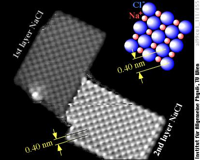
22 Imaging single crystal lattice: NaCl The aluminum supporting is shown black.
23 A case study of atomic imaging Conversion of carbon mono-oxide (CO) to carbon dioxide (CO 2 ) Numerous applications in mining safety, vehicle exhaust treatment, carbon dioxide lasers, etc. Must be operated at room temperature. Cost effective: current catalysts are mostly based on precious metals like platinum. Development of new catalysts demands exploration of surface reaction mechanism, especially at atomic sacle. L. Zang, & H. Kisch Angew. Chem. Int. Ed. 2000, 39, German Patent (DE ).
24 Room Temperature Oxidation of CO over Amorphous Nanocrystalline RuO 2 CO + O 2 CO 2 RuO 2 No significant loss of activity after 5 cycles L. Zang, & H. Kisch Angew. Chem. Int. Ed. 2000, 39, German Patent (DE ).
 Surface Ru-cus: coordinatively unsaturated sites CO + cus CO-cus O 2 + 2cus 2O-cus CO-cus + O-cus CO")
25 K. Jacobi, H. Over & G. Ertl et al. Science 2000, 287, J. Am. Chem. Soc. 2001, 123, J. Phys. Chem. B, 2002, 106, Ball-and-Stick Model of the RuO 2 (110) Surface Ru-cus: coordinatively unsaturated sites CO + cus CO-cus O 2 + 2cus 2O-cus CO-cus + O-cus CO 2 + 2cus
 and its rectangular unit cell.")
26 STM probing of RuO 2 single-crystal surface On the left side, RuO 2 (110) domains are visible. The magnified inset shows the internal structure of this phase (parallel rows along the [001] direction) and its rectangular unit cell. The right side represents a domain of the Ru(0001)-(1 1)- O surface; The magnified inset reveals a hexagonal arrangement of dots corresponding to the Ru(0001) lattice. The dark spots mark the locations of the chemisorbed O atoms in the (1 1) overlayer. The bright spots represent Ru atoms coordinated to three O atoms. Large-scale STM image (1000 Å by 1000 Å) together with enlargements (50 Å by 50 Å) as insets. Tunneling parameters are U = 1.21 V and 0.46 na Science, Vol 287, Issue 5457,
. STM image (200 Å by 200 Å, U = 0.82 V, I = 3.")
27 STM probing of RuO 2 single-crystal surface deposited with CO STM image (200 Å by 200 Å, U = 1.08 V, I = 0.46 na, constant current mode) of the RuO2(110) surface after exposure of 10-layer of CO. The CO molecules are imaged as bright protrusions with an apparent height of 0.5 Å. The CO molecules are sitting between the bright rows (Ru). STM image (200 Å by 200 Å, U = 0.82 V, I = 3.34 na) of the CO-covered RuO2(110) surface of after annealing to 600 K. The removal of CO molecules is accompanied by the creation of 1.5 Å to 3.0 Å deep holes --- vacancies, due to the partial removal of O atoms from the substrate lattice by reaction with CO. Science, Vol 287, Issue 5457,

28 Excellent Agreement between Ambient and UHV: Arrhenius plot Open square: RuO 2 particle Solid circle: RuO 2 (100) crystal surface. The absolute pressure of CO & O 2 differed by about 10 orders of magnitude! Note: Only the slope (activation energy) holds for the interest of agreement, as the absolute Y scale should be related to the active surface area. Y-axis is given in arbitrary units on which both sets of data were arbitrarily displaced vertically until best agreement was reached. K. Jacobi, & G. Ertl et al. J. Phys. Chem. B, 2002, 106, L. Zang, & H. Kisch Angew. Chem. Int. Ed. 2000, 39, German Patent (DE ).

29 Real surface of Gold Gold surface, 120X120 nm, 4K, no atomic structure Be careful --- When you try to say you got a flat surface.

30 Real atomic flat! Atomically flat Au film

31 STM does good job for imaging metal cluster 2-D network of 4 nm Au cluster array on GaAs

32 STM does good job for imaging metal cluster 3-D piling of 2 nm Au clusters

33 Shape control of transition metal nanoparticles Why control the shape? Non-linear optical properties; Surface enhanced Raman; Catalysis. (George Schatz work at NW) Au triangles on MoS2
, and deposition of vanadium metal thereon; (b) 0.03 ML(monolayer), (c) 0.")
34 Single crystalline Titanium oxide: doping of vanadium STM images obtained for (a) clean TiO2(110), and deposition of vanadium metal thereon; (b) 0.03 ML(monolayer), (c) 0.25 ML, (d) 2.0 ML.
 and octahedral- Fe terminated (b) Fe3O4(001).")
35 Iron oxides: important materials for recording Atomically resolved STM images of tetrahedral-fe terminated (a) and octahedral- Fe terminated (b) Fe3O4(001).

36 STM exploration of physical properties Atoms of n-type MoS2 --- a common dry lubricant. The bright spots indicate S atoms, which account for its excellent lubrication properties.

")
37 Imaging organic reaction on surface Physisorbed pyridine and pyridineoxide at a Cu(110) surface 3D representation of an STM image of Pyridine oxide at a Cu(110) surface
Special Properties of Au Nanoparticles
 Special Properties of Au Nanoparticles Maryam Ebrahimi Chem 7500/750 March 28 th, 2007 1 Outline Introduction The importance of unexpected electronic, geometric, and chemical properties of nanoparticles
Lecture 30: Kinetics of Epitaxial Growth: Surface Diffusion and
 Lecture 30: Kinetics of Epitaxial Growth: Surface Diffusion and Nucleation Today s topics Understanding the basics of epitaxial techniques used for surface growth of crystalline structures (films, or layers).
Catalysis by supported metal clusters and model systems
 Catalysis by supported metal clusters and model systems Gianfranco Pacchioni Dipartimento di Scienza dei Materiali Università Milano-Bicocca Part I Catalysis by supported metal clusters and model systems
Supplementary Figure 1 Experimental setup for crystal growth. Schematic drawing of the experimental setup for C 8 -BTBT crystal growth.
 Supplementary Figure 1 Experimental setup for crystal growth. Schematic drawing of the experimental setup for C 8 -BTBT crystal growth. Supplementary Figure 2 AFM study of the C 8 -BTBT crystal growth
SUPPLEMENTARY INFORMATION
 DOI: 10.1038/NCHEM.2491 Experimental Realization of Two-dimensional Boron Sheets Baojie Feng 1, Jin Zhang 1, Qing Zhong 1, Wenbin Li 1, Shuai Li 1, Hui Li 1, Peng Cheng 1, Sheng Meng 1,2, Lan Chen 1 and
Catalysis. Catalytic nanoparticles have been used for centuries to facilitate desirable chemical reactions and to suppress unwanted byproducts.
 Catalysis Catalytic nanoparticles have been used for centuries to facilitate desirable chemical reactions and to suppress unwanted byproducts. Gerhard Ertl received the 2007 Chemistry Nobel Prize for converting
Graphene. Tianyu Ye November 30th, 2011
 Graphene Tianyu Ye November 30th, 2011 Outline What is graphene? How to make graphene? (Exfoliation, Epitaxial, CVD) Is it graphene? (Identification methods) Transport properties; Other properties; Applications;
Università degli Studi di Bari "Aldo Moro"
 Università degli Studi di Bari "Aldo Moro" Table of contents 1. Introduction to Atomic Force Microscopy; 2. Introduction to Raman Spectroscopy; 3. The need for a hybrid technique Raman AFM microscopy;
Module 5: "Adsoption" Lecture 25: The Lecture Contains: Definition. Applications. How does Adsorption occur? Physisorption Chemisorption.
 The Lecture Contains: Definition Applications How does Adsorption occur? Physisorption Chemisorption Energetics Adsorption Isotherms Different Adsorption Isotherms Langmuir Adsorption Isotherm file:///e
STM spectroscopy (STS)
") STM spectroscopy (STS) di dv 4 e ( E ev, r) ( E ) M S F T F Basic concepts of STS. With the feedback circuit open the variation of the tunneling current due to the application of a small oscillating voltage
STM spectroscopy (STS) di dv 4 e ( E ev, r) ( E ) M S F T F Basic concepts of STS. With the feedback circuit open the variation of the tunneling current due to the application of a small oscillating voltage
Water clustering on nanostructured iron oxide films
 ARTICLE Received 12 May 2013 Accepted 22 May 2014 Published 30 Jun 2014 Water clustering on nanostructured iron oxide films Lindsay R. Merte1,2, Ralf Bechstein1, W. Guowen Peng3, Felix Rieboldt1, Carrie
Lecture 4 Scanning Probe Microscopy (SPM)
") Lecture 4 Scanning Probe Microscopy (SPM) General components of SPM; Tip --- the probe; Cantilever --- the indicator of the tip; Tip-sample interaction --- the feedback system; Scanner --- piezoelectric
Lecture 4 Scanning Probe Microscopy (SPM) General components of SPM; Tip --- the probe; Cantilever --- the indicator of the tip; Tip-sample interaction --- the feedback system; Scanner --- piezoelectric
High-resolution Characterization of Organic Ultrathin Films Using Atomic Force Microscopy
 High-resolution Characterization of Organic Ultrathin Films Using Atomic Force Microscopy Jing-jiang Yu Nanotechnology Measurements Division Agilent Technologies, Inc. Atomic Force Microscopy High-Resolution
Scanning Tunneling Microscopy and its Application
 Chunli Bai Scanning Tunneling Microscopy and its Application With 181 Figures SHANGHAI SCIENTIFIC & TECHNICAL PUBLISHERS Jpl Springer Contents 1. Introduction 1 1.1 Advantages of STM Compared with Other
Crystalline Surfaces for Laser Metrology
 Crystalline Surfaces for Laser Metrology A.V. Latyshev, Institute of Semiconductor Physics SB RAS, Novosibirsk, Russia Abstract: The number of methodological recommendations has been pronounced to describe
Surface Science (Chemistry)
") Surface Science Mankind has studied surface and interface phenomena since antiquity. In old Babylon a form of divination, called lecanomancy, involved an examination of the properties of oil poured into
Surface Science Mankind has studied surface and interface phenomena since antiquity. In old Babylon a form of divination, called lecanomancy, involved an examination of the properties of oil poured into
Surface atoms/molecules of a material act as an interface to its surrounding environment;
 1 Chapter 1 Thesis Overview Surface atoms/molecules of a material act as an interface to its surrounding environment; their properties are often complicated by external adsorbates/species on the surface
Chem 728 Introduction to Solid Surfaces
 Chem 728 Introduction to Solid Surfaces Solids: hard; fracture; not compressible; molecules close to each other Liquids: molecules mobile, but quite close to each other Gases: molecules very mobile; compressible
SUPPLEMENTARY INFORMATION
 In the format provided by the authors and unedited. Intrinsically patterned two-dimensional materials for selective adsorption of molecules and nanoclusters X. Lin 1,, J. C. Lu 1,, Y. Shao 1,, Y. Y. Zhang
Graphene films on silicon carbide (SiC) wafers supplied by Nitride Crystals, Inc.
 wafers supplied by Nitride Crystals, Inc.") 9702 Gayton Road, Suite 320, Richmond, VA 23238, USA Phone: +1 (804) 709-6696 info@nitride-crystals.com www.nitride-crystals.com Graphene films on silicon carbide (SiC) wafers supplied by Nitride Crystals,
9702 Gayton Road, Suite 320, Richmond, VA 23238, USA Phone: +1 (804) 709-6696 info@nitride-crystals.com www.nitride-crystals.com Graphene films on silicon carbide (SiC) wafers supplied by Nitride Crystals,
Introduction to Nanotechnology Chapter 5 Carbon Nanostructures Lecture 1
 Introduction to Nanotechnology Chapter 5 Carbon Nanostructures Lecture 1 ChiiDong Chen Institute of Physics, Academia Sinica chiidong@phys.sinica.edu.tw 02 27896766 Carbon contains 6 electrons: (1s) 2,
REPORT ON SCANNING TUNNELING MICROSCOPE. Course ME-228 Materials and Structural Property Correlations Course Instructor Prof. M. S.
 REPORT ON SCANNING TUNNELING MICROSCOPE Course ME-228 Materials and Structural Property Correlations Course Instructor Prof. M. S. Bobji Submitted by Ankush Kumar Jaiswal (09371) Abhay Nandan (09301) Sunil
Scanning Tunneling Microscopy Studies of the Ge(111) Surface
 Surface") VC Scanning Tunneling Microscopy Studies of the Ge(111) Surface Anna Rosen University of California, Berkeley Advisor: Dr. Shirley Chiang University of California, Davis August 24, 2007 Abstract: This
VC Scanning Tunneling Microscopy Studies of the Ge(111) Surface Anna Rosen University of California, Berkeley Advisor: Dr. Shirley Chiang University of California, Davis August 24, 2007 Abstract: This
Shell-isolated nanoparticle-enhanced Raman spectroscopy
 Shell-isolated nanoparticle-enhanced Raman spectroscopy Jian Feng Li, Yi Fan Huang, Yong Ding, Zhi Lin Yang, Song Bo Li, Xiao Shun Zhou, Feng Ru Fan, Wei Zhang, Zhi You Zhou, De Yin Wu, Bin Ren, Zhong
Scanning Tunneling Microscopy. how does STM work? the quantum mechanical picture example of images how can we understand what we see?
 Scanning Tunneling Microscopy how does STM work? the quantum mechanical picture example of images how can we understand what we see? Observation of adatom diffusion with a field ion microscope Scanning
a b c Supplementary Figure S1
 a b c Supplementary Figure S1 AFM measurements of MoS 2 nanosheets prepared from the electrochemical Liintercalation and exfoliation. (a) AFM measurement of a typical MoS 2 nanosheet, deposited on Si/SiO
Hydrogenation of Single Walled Carbon Nanotubes
 Hydrogenation of Single Walled Carbon Nanotubes Anders Nilsson Stanford Synchrotron Radiation Laboratory (SSRL) and Stockholm University Coworkers and Ackowledgement A. Nikitin 1), H. Ogasawara 1), D.
NTEGRA for EC PRESENTATION
 NTEGRA for EC PRESENTATION Application Purpose: In-situ control/modification of the surface morphology of single crystal and polycrystal electrodes (samples) during electrochemical process (in situ) in
2) Atom manipulation. Xe / Ni(110) Model: Experiment:
 Atom manipulation. Xe / Ni(110) Model: Experiment:") 2) Atom manipulation D. Eigler & E. Schweizer, Nature 344, 524 (1990) Xe / Ni(110) Model: Experiment: G.Meyer, et al. Applied Physics A 68, 125 (1999) First the tip is approached close to the adsorbate
2) Atom manipulation D. Eigler & E. Schweizer, Nature 344, 524 (1990) Xe / Ni(110) Model: Experiment: G.Meyer, et al. Applied Physics A 68, 125 (1999) First the tip is approached close to the adsorbate
Lecture 10 Thin Film Growth
 Lecture 10 Thin Film Growth 1/76 Announcements Homework: Homework Number 2 is returned today, please pick it up from me at the end of the class. Solutions are online. Homework 3 will be set Thursday (2
Nanostructure. Materials Growth Characterization Fabrication. More see Waser, chapter 2
 Nanostructure Materials Growth Characterization Fabrication More see Waser, chapter 2 Materials growth - deposition deposition gas solid Physical Vapor Deposition Chemical Vapor Deposition Physical Vapor
General concept and defining characteristics of AFM. Dina Kudasheva Advisor: Prof. Mary K. Cowman
 General concept and defining characteristics of AFM Dina Kudasheva Advisor: Prof. Mary K. Cowman Overview Introduction History of the SPM invention Technical Capabilities Principles of operation Examples
From manipulation of the charge state to imaging of individual molecular orbitals and bond formation
 Scanning Probe Microscopy of Adsorbates on Insulating Films: From manipulation of the charge state to imaging of individual molecular orbitals and bond formation Gerhard Meyer, Jascha Repp, Peter Liljeroth
Surface Studies by Scanning Tunneling Microscopy
 Surface Studies by Scanning Tunneling Microscopy G. Binnig, H. Rohrer, Ch. Gerber, and E. Weibel IBM Zurich Research Laboratory, 8803 Ruschlikon-ZH, Switzerland (Received by Phys. Rev. Lett. on 30th April,
Solid Surfaces, Interfaces and Thin Films
 Hans Lüth Solid Surfaces, Interfaces and Thin Films Fifth Edition With 427 Figures.2e Springer Contents 1 Surface and Interface Physics: Its Definition and Importance... 1 Panel I: Ultrahigh Vacuum (UHV)
Concepts in Surface Physics
 M.-C. Desjonqueres D. Spanjaard Concepts in Surface Physics Second Edition With 257 Figures Springer 1. Introduction................................. 1 2. Thermodynamical and Statistical Properties of
Nanoscale Surface Physics PHY 5XXX
 SYLLABUS Nanoscale Surface Physics PHY 5XXX Spring Semester, 2006 Instructor: Dr. Beatriz Roldán-Cuenya Time: Tuesday and Thursday 4:00 to 5:45 pm Location: Theory: MAP 306, Laboratory: MAP 148 Office
Recent applications of nanostructured materials - from solar cells and batteries to biological markers
 Recent applications of nanostructured materials - from solar cells and batteries to biological markers Prof. Jan Augustyński o Origins of nanotechnology - limits of miniaturization. o Nanoparticle size
SUPPLEMENTARY FIGURES
 1 SUPPLEMENTARY FIGURES Supplementary Figure 1: Initial stage showing monolayer MoS 2 islands formation on Au (111) surface. a, Scanning tunneling microscopy (STM) image of molybdenum (Mo) clusters deposited
Nanostructure Fabrication Using Selective Growth on Nanosize Patterns Drawn by a Scanning Probe Microscope
 Nanostructure Fabrication Using Selective Growth on Nanosize Patterns Drawn by a Scanning Probe Microscope Kentaro Sasaki, Keiji Ueno and Atsushi Koma Department of Chemistry, The University of Tokyo,
8 Summary and outlook
 91 8 Summary and outlook The main task of present work was to investigate the growth, the atomic and the electronic structures of Co oxide as well as Mn oxide films on Ag(001) by means of STM/STS at LT
Molecular Ordering at the Interface Between Liquid Water and Rutile TiO 2 (110)
") Molecular Ordering at the Interface Between Liquid Water and Rutile TiO 2 (110) B E A T R I C E B O N A N N I D i p a r t i m e n t o d i F i s i c a, U n i v e r s i t a di R o m a T o r V e r g a t a
Molecular Ordering at the Interface Between Liquid Water and Rutile TiO 2 (110) B E A T R I C E B O N A N N I D i p a r t i m e n t o d i F i s i c a, U n i v e r s i t a di R o m a T o r V e r g a t a
Designing Graphene for Hydrogen Storage
 Designing Graphene for Hydrogen Storage Stefan Heun NEST, Istituto Nanoscienze-CNR and Scuola Normale Superiore Pisa, Italy Outline Introduction to Hydrogen Storage Epitaxial Graphene Hydrogen Storage
Molecular Dynamics on the Angstrom Scale
 Probing Interface Reactions by STM: Molecular Dynamics on the Angstrom Scale Zhisheng Li Prof. Richard Osgood Laboratory for Light-Surface Interactions, Columbia University Outline Motivation: Why do we
Solids. properties & structure
 Solids properties & structure Determining Crystal Structure crystalline solids have a very regular geometric arrangement of their particles the arrangement of the particles and distances between them is
Supplementary Materials for
 advances.sciencemag.org/cgi/content/full/3/10/e1701661/dc1 Supplementary Materials for Defect passivation of transition metal dichalcogenides via a charge transfer van der Waals interface Jun Hong Park,
Self-Assembly of Two-Dimensional Organic Networks Containing Heavy Metals (Pb, Bi) and Preparation of Spin-Polarized Scanning Tunneling Microscope
 and Preparation of Spin-Polarized Scanning Tunneling Microscope") MPhil Thesis Defense Self-Assembly of Two-Dimensional Organic Networks Containing Heavy Metals (Pb, Bi) and Preparation of Spin-Polarized Scanning Tunneling Microscope Presented by CHEN Cheng 12 th Aug.
MPhil Thesis Defense Self-Assembly of Two-Dimensional Organic Networks Containing Heavy Metals (Pb, Bi) and Preparation of Spin-Polarized Scanning Tunneling Microscope Presented by CHEN Cheng 12 th Aug.
1 Introduction COPYRIGHTED MATERIAL. 1.1 HowdoweDefinetheSurface?
 1 Introduction JOHN C. VICKERMAN Manchester Interdisciplinary Biocentre, School of Chemical Engineering and Analytical Science, The University of Manchester, Manchester, UK The surface behaviour of materials
SUPPLEMENTARY INFORMATION
 Lateral heterojunctions within monolayer MoSe 2 -WSe 2 semiconductors Chunming Huang 1,#,*, Sanfeng Wu 1,#,*, Ana M. Sanchez 2,#,*, Jonathan J. P. Peters 2, Richard Beanland 2, Jason S. Ross 3, Pasqual
Introduction to Nanotechnology Chapter 5 Carbon Nanostructures Lecture 1
 Introduction to Nanotechnology Chapter 5 Carbon Nanostructures Lecture 1 ChiiDong Chen Institute of Physics, Academia Sinica chiidong@phys.sinica.edu.tw 02 27896766 Section 5.2.1 Nature of the Carbon Bond
Reactions at solid surfaces: From atoms to complexity. Gerhard Ertl Fritz Haber Institut der Max Planck-Gesellschaft Berlin, Germany
 Reactions at solid surfaces: From atoms to complexity Gerhard Ertl Fritz Haber Institut der Max Planck-Gesellschaft Berlin, Germany Jöns Jakob Berzelius 1779 1848 Wilhelm Ostwald 1853 1932 Nobel Prize
SUPPLEMENTARY INFORMATION
 SUPPLEMENTARY INFORMATION Towards wafer-size graphene layers by atmospheric pressure graphitization of silicon carbide Supporting online material Konstantin V. Emtsev 1, Aaron Bostwick 2, Karsten Horn
Experimental methods in physics. Local probe microscopies I
 Experimental methods in physics Local probe microscopies I Scanning tunnelling microscopy (STM) Jean-Marc Bonard Academic year 09-10 1. Scanning Tunneling Microscopy 1.1. Introduction Image of surface
Initial Stages of Growth of Organic Semiconductors on Graphene
 Initial Stages of Growth of Organic Semiconductors on Graphene Presented by: Manisha Chhikara Supervisor: Prof. Dr. Gvido Bratina University of Nova Gorica Outline Introduction to Graphene Fabrication
Nanostructures. Lecture 13 OUTLINE
 Nanostructures MTX9100 Nanomaterials Lecture 13 OUTLINE -What is quantum confinement? - How can zero-dimensional materials be used? -What are one dimensional structures? -Why does graphene attract so much
Imaging Methods: Scanning Force Microscopy (SFM / AFM)
") Imaging Methods: Scanning Force Microscopy (SFM / AFM) The atomic force microscope (AFM) probes the surface of a sample with a sharp tip, a couple of microns long and often less than 100 Å in diameter.
Imaging Methods: Scanning Force Microscopy (SFM / AFM) The atomic force microscope (AFM) probes the surface of a sample with a sharp tip, a couple of microns long and often less than 100 Å in diameter.
MSE8210 Advanced Topics in Theoretical Surface and Interface Science
 MSE8210 Advanced Topics in Theoretical Surface and Interface Science Aloysius Soon 알로이시우스손 aloysius.soon@yonsei.ac.kr Course outline An introduction to fundamental concepts in theoretical surface science
Supporting Information
 Supporting Information Yao et al. 10.1073/pnas.1416368111 Fig. S1. In situ LEEM imaging of graphene growth via chemical vapor deposition (CVD) on Pt(111). The growth of graphene on Pt(111) via a CVD process
CITY UNIVERSITY OF HONG KONG. Theoretical Study of Electronic and Electrical Properties of Silicon Nanowires
 CITY UNIVERSITY OF HONG KONG Ë Theoretical Study of Electronic and Electrical Properties of Silicon Nanowires u Ä öä ªqk u{ Submitted to Department of Physics and Materials Science gkö y in Partial Fulfillment
A nanoscale perspective on the effect of acid washing of carbon catalyst supports
 A nanoscale perspective on the effect of acid washing of carbon catalyst supports Emir Bouleghlimat, Philip R. Davies, Robert J. Davies, Jiri Kulahvy, David J. Morgan, School of Chemistry, Cardiff University
Institut des NanoSciences de Paris
 CNRS / Photothèque Cyril Frésillon Institut des NanoSciences de Paris Polarity in low dimensions: MgO nano-ribbons on Au(111) J. Goniakowski, C. Noguera Institut des Nanosciences de Paris, CNRS & Université
Quantum Condensed Matter Physics Lecture 12
 Quantum Condensed Matter Physics Lecture 12 David Ritchie QCMP Lent/Easter 2016 http://www.sp.phy.cam.ac.uk/drp2/home 12.1 QCMP Course Contents 1. Classical models for electrons in solids 2. Sommerfeld
Wafer holders. Mo- or Ta- made holders Bonding: In (Ga), or In-free (clamped) Quick and easy transfer
, or In-free (clamped) Quick and easy transfer") Wafer holders Mo- or Ta- made holders Bonding: In (Ga), or In-free (clamped) Quick and easy transfer Image: In-free, 3-inch sample holder fitting a quarter of a 2- inch wafer Reflection High Energy Electron
Wafer holders Mo- or Ta- made holders Bonding: In (Ga), or In-free (clamped) Quick and easy transfer Image: In-free, 3-inch sample holder fitting a quarter of a 2- inch wafer Reflection High Energy Electron
Mater. Res. Soc. Symp. Proc. Vol Materials Research Society
 Mater. Res. Soc. Symp. Proc. Vol. 1217 2010 Materials Research Society 1217-Y08-43 Surface Structure of Pd 3 Fe(111) and Effects of Oxygen Adsorption Xiaofang Yang, Lindsey A. Welch, Jie Fu and Bruce E.
672 Advanced Solid State Physics. Scanning Tunneling Microscopy
 672 Advanced Solid State Physics Scanning Tunneling Microscopy Biao Hu Outline: 1. Introduction to STM 2. STM principle & working modes 3. STM application & extension 4. STM in our group 1. Introduction
29: Nanotechnology. What is Nanotechnology? Properties Control and Understanding. Nanomaterials
 29: Nanotechnology What is Nanotechnology? Properties Control and Understanding Nanomaterials Making nanomaterials Seeing at the nanoscale Quantum Dots Carbon Nanotubes Biology at the Nanoscale Some Applications
Scanning Tunneling Microscopy (STM)
") Page 1 of 8 Scanning Tunneling Microscopy (STM) This is the fastest growing surface analytical technique, which is replacing LEED as the surface imaging tool (certainly in UHV, air and liquid). STM has
Page 1 of 8 Scanning Tunneling Microscopy (STM) This is the fastest growing surface analytical technique, which is replacing LEED as the surface imaging tool (certainly in UHV, air and liquid). STM has
Surface Sensitivity & Surface Specificity
 Surface Sensitivity & Surface Specificity The problems of sensitivity and detection limits are common to all forms of spectroscopy. In its simplest form, the question of sensitivity boils down to whether
Supplementary Figure 1 Morpholigical properties of TiO 2-x SCs. The statistical particle size distribution (a) of the defective {001}-TiO 2-x SCs and
 of the defective {001}-TiO 2-x SCs and") Supplementary Figure 1 Morpholigical properties of TiO 2-x s. The statistical particle size distribution (a) of the defective {1}-TiO 2-x s and their typical TEM images (b, c). Quantity Adsorbed (cm 3
Supplementary Figure 1 Morpholigical properties of TiO 2-x s. The statistical particle size distribution (a) of the defective {1}-TiO 2-x s and their typical TEM images (b, c). Quantity Adsorbed (cm 3
The first three categories are considered a bottom-up approach while lithography is a topdown
 Nanowires and Nanorods One-dimensional structures have been called in different ways: nanowires, nanorod, fibers of fibrils, whiskers, etc. The common characteristic of these structures is that all they
MSE 321 Structural Characterization
 Auger Spectroscopy Auger Electron Spectroscopy (AES) Scanning Auger Microscopy (SAM) Incident Electron Ejected Electron Auger Electron Initial State Intermediate State Final State Physical Electronics
STM and graphene. W. W. Larry Pai ( 白偉武 ) Center for condensed matter sciences, National Taiwan University NTHU, 2013/05/23
 Center for condensed matter sciences, National Taiwan University NTHU, 2013/05/23") STM and graphene W. W. Larry Pai ( 白偉武 ) Center for condensed matter sciences, National Taiwan University NTHU, 2013/05/23 Why graphene is important: It is a new form of material (two dimensional, single
STM and graphene W. W. Larry Pai ( 白偉武 ) Center for condensed matter sciences, National Taiwan University NTHU, 2013/05/23 Why graphene is important: It is a new form of material (two dimensional, single
INTRODUCTION TO SCA\ \I\G TUNNELING MICROSCOPY
 INTRODUCTION TO SCA\ \I\G TUNNELING MICROSCOPY SECOND EDITION C. JULIAN CHEN Department of Applied Physics and Applied Mathematics, Columbia University, New York OXFORD UNIVERSITY PRESS Contents Preface
The design of an integrated XPS/Raman spectroscopy instrument for co-incident analysis
 The design of an integrated XPS/Raman spectroscopy instrument for co-incident analysis Tim Nunney The world leader in serving science 2 XPS Surface Analysis XPS +... UV Photoelectron Spectroscopy UPS He(I)
Solutions for Assignment-8
 Solutions for Assignment-8 Q1. The process of adding impurities to a pure semiconductor is called: [1] (a) Mixing (b) Doping (c) Diffusing (d) None of the above In semiconductor production, doping intentionally
1. Robust hexagonal rings on Cu(111) Figure S1 2. Details of Monte Carlo simulations
 Figure S1 2. Details of Monte Carlo simulations") Supporting Information for Influence of Relativistic Effects on Assembled Structures of V-Shaped Bispyridine Molecules on M(111) Surfaces where M = Cu, Ag, Au Xue Zhang, 1,ǁ Na Li, 1, Hao Wang, 1 Chenyang
Supporting Information for Influence of Relativistic Effects on Assembled Structures of V-Shaped Bispyridine Molecules on M(111) Surfaces where M = Cu, Ag, Au Xue Zhang, 1,ǁ Na Li, 1, Hao Wang, 1 Chenyang
MODERN TECHNIQUES OF SURFACE SCIENCE
 MODERN TECHNIQUES OF SURFACE SCIENCE Second edition D. P. WOODRUFF & T. A. DELCHAR Department ofphysics, University of Warwick CAMBRIDGE UNIVERSITY PRESS Contents Preface to first edition Preface to second
Spectroscopy at nanometer scale
 Spectroscopy at nanometer scale 1. Physics of the spectroscopies 2. Spectroscopies for the bulk materials 3. Experimental setups for the spectroscopies 4. Physics and Chemistry of nanomaterials Various
Application of single crystalline tungsten for fabrication of high resolution STM probes with controlled structure 1
 Application of single crystalline tungsten for fabrication of high resolution STM probes with controlled structure 1 A. N. Chaika a, S. S. Nazin a, V. N. Semenov a, V. G. Glebovskiy a, S. I. Bozhko a,b,
Supplementary Figure 1. (a-b) EDX of Mo 2 and Mo 2
 EDX of Mo 2 and Mo 2") Supplementary Figure 1. (a-b) EDX of Mo 2 C@NPC/NPRGO and Mo 2 C@NPC. Supplementary Figure 2. (a) SEM image of PMo 12 2-PPy, (b) TEM, (c) HRTEM, (d) STEM image and EDX elemental mapping of C, N, P, and
Supplementary Figure 1. (a-b) EDX of Mo 2 C@NPC/NPRGO and Mo 2 C@NPC. Supplementary Figure 2. (a) SEM image of PMo 12 2-PPy, (b) TEM, (c) HRTEM, (d) STEM image and EDX elemental mapping of C, N, P, and
Supplementary information
 Supplementary information Supplementary Figure S1STM images of four GNBs and their corresponding STS spectra. a-d, STM images of four GNBs are shown in the left side. The experimental STS data with respective
Seminars in Nanosystems - I
 Seminars in Nanosystems - I Winter Semester 2011/2012 Dr. Emanuela Margapoti Emanuela.Margapoti@wsi.tum.de Dr. Gregor Koblmüller Gregor.Koblmueller@wsi.tum.de Seminar Room at ZNN 1 floor Topics of the
Chapter 2 Surface Science Studies of Metal Oxide Gas Sensing Materials
 Chapter 2 Surface Science Studies of Metal Oxide Gas Sensing Materials Junguang Tao and Matthias Batzill Abstract In this chapter we present recent advances in the study of metal oxide surfaces and put
Surface Physics Surface Diffusion. Assistant: Dr. Enrico Gnecco NCCR Nanoscale Science
 Surface Physics 008 8. Surface Diffusion Assistant: Dr. Enrico Gnecco NCCR Nanoscale Science Random-Walk Motion Thermal motion of an adatom on an ideal crystal surface: - Thermal excitation the adatom
Spectroscopy of Nanostructures. Angle-resolved Photoemission (ARPES, UPS)
") Spectroscopy of Nanostructures Angle-resolved Photoemission (ARPES, UPS) Measures all quantum numbers of an electron in a solid. E, k x,y, z, point group, spin E kin, ϑ,ϕ, hν, polarization, spin Electron
Spectroscopy of Nanostructures Angle-resolved Photoemission (ARPES, UPS) Measures all quantum numbers of an electron in a solid. E, k x,y, z, point group, spin E kin, ϑ,ϕ, hν, polarization, spin Electron
Fabrication at the nanoscale for nanophotonics
 Fabrication at the nanoscale for nanophotonics Ilya Sychugov, KTH Materials Physics, Kista silicon nanocrystal by electron beam induced deposition lithography Outline of basic nanofabrication methods Devices
Scanning Probe Microscopy. Amanda MacMillan, Emmy Gebremichael, & John Shamblin Chem 243: Instrumental Analysis Dr. Robert Corn March 10, 2010
 Scanning Probe Microscopy Amanda MacMillan, Emmy Gebremichael, & John Shamblin Chem 243: Instrumental Analysis Dr. Robert Corn March 10, 2010 Scanning Probe Microscopy High-Resolution Surface Analysis
Cover Page. The handle holds various files of this Leiden University dissertation
 Cover Page The handle http://hdl.handle.net/1887/29891 holds various files of this Leiden University dissertation Author: Roobol, Sander Bas Title: The structure of a working catalyst : from flat surfaces
Physics 9826: Surface Science. Textbooks
 Physics 9826: Surface Science Winter 2013 Lectures: Monday, 10:30 am 12:30 pm P&A B 26 Wednesday, 10:30am-11:30am P&A B 26 Office hours: by appointment, PAB 231 Web-site: http://www.physics.uwo.ca/~lgonchar/courses/p9826/index.shtml
Energy level alignment and two-dimensional structure of pentacene on Au 111 surfaces
 JOURNAL OF APPLIED PHYSICS VOLUME 91, NUMBER 5 1 MARCH 2002 Energy level alignment and two-dimensional structure of pentacene on Au 111 surfaces P. G. Schroeder, C. B. France, J. B. Park, and B. A. Parkinson
Pb thin films on Si(111): Local density of states and defects
: Local density of states and defects") University of Wollongong Research Online Australian Institute for Innovative Materials - Papers Australian Institute for Innovative Materials 2014 Pb thin films on Si(111): Local density of states and
University of Wollongong Research Online Australian Institute for Innovative Materials - Papers Australian Institute for Innovative Materials 2014 Pb thin films on Si(111): Local density of states and
The Use of Synchrotron Radiation in Modern Research
 The Use of Synchrotron Radiation in Modern Research Physics Chemistry Structural Biology Materials Science Geochemical and Environmental Science Atoms, molecules, liquids, solids. Electronic and geometric
A new method of growing graphene on Cu by hydrogen etching
 A new method of growing graphene on Cu by hydrogen etching Linjie zhan version 6, 2015.05.12--2015.05.24 CVD graphene Hydrogen etching Anisotropic Copper-catalyzed Highly anisotropic hydrogen etching method
Adsorption, desorption, and diffusion on surfaces. Joachim Schnadt Divsion of Synchrotron Radiation Research Department of Physics
 Adsorption, desorption, and diffusion on surfaces Joachim Schnadt Divsion of Synchrotron Radiation Research Department of Physics Adsorption and desorption Adsorption Desorption Chemisorption: formation
Adsorption energetics of CO on supported Pd nanoparticles as a function of particle size by single crystal microcalorimetry
 PCCP Dynamic Article Links View Online Cite this: DOI: 10.1039/c1cp21677e www.rsc.org/pccp PAPER Adsorption energetics of CO on supported Pd nanoparticles as a function of particle size by single crystal
Physics and Chemistry of Interfaces
 Hans Jürgen Butt, Karlheinz Graf, and Michael Kappl Physics and Chemistry of Interfaces Second, Revised and Enlarged Edition WILEY- VCH WILEY-VCH Verlag GmbH & Co. KGaA Contents Preface XI 1 Introduction
Chemical Processes on Solid Surfaces
 10 October 2007 Scientific Background on the Nobel Prize in Chemistry 2007 Chemical Processes on Solid Surfaces The Royal Swedish Academy of Sciences, Information Department, Box 50005, SE-104 05 Stockholm,
Supporting Information. for. Angew. Chem. Int. Ed. Z Wiley-VCH 2003
 Supporting Information for Angew. Chem. Int. Ed. Z52074 Wiley-VCH 2003 69451 Weinheim, Germany Kinetic and Thermodynamic Control via Chemical Bond Rearrangement on Si(001) Surface Chiho Hamai, Akihiko
Photovoltage phenomena in nanoscaled materials. Thomas Dittrich Hahn-Meitner-Institute Berlin
 Photovoltage phenomena in nanoscaled materials Thomas Dittrich Hahn-Meitner-Institute Berlin 1 2 Introduction From bulk to nanostructure: SPV on porous Si Retarded SPV response and its origin Photovoltage
Gregory S. Rohrer,* Victor E. Henrich, Dawn A. Bonnell
 Structure of the Reduced TiO 2 (110) Surface Determined by Scanning Tunneling Microscopy Gregory S. Rohrer,* Victor E. Henrich, Dawn A. Bonnell The scanning tunneling microscope has been used to image