Precision Electrolytic Nanofabrication
|
|
|
- Percival Thornton
- 5 years ago
- Views:
Transcription
1 University of Tennessee, Knoxville Trace: Tennessee Research and Creative Exchange University of Tennessee Honors Thesis Projects University of Tennessee Honors Program Spring Precision Electrolytic Nanofabrication Kent Cooksey Wilcher University of Tennessee - Knoxville Follow this and additional works at: Recommended Citation Wilcher, Kent Cooksey, "Precision Electrolytic Nanofabrication" (2002). University of Tennessee Honors Thesis Projects. This is brought to you for free and open access by the University of Tennessee Honors Program at Trace: Tennessee Research and Creative Exchange. It has been accepted for inclusion in University of Tennessee Honors Thesis Projects by an authorized administrator of Trace: Tennessee Research and Creative Exchange. For more information, please contact trace@utk.edu.
2 Precision Electrolytic Nanofabrication Kent Wilcher Senior Honors Project The University of Tennessee, Knoxville Oak Ridge National Laboratory Knoxville, TN Submitted: May 03,2002
3 11 Table of Contents Abstract iii Introduction 1 Methods and Materials 2 Results 4 Discussion and Conclusions 8 Acknowledgments 9 References 10 Figures 11 Tables 21

4 111 Abstract The ability to manipulate individual molecules is of fundamental importance in the development of the next generation of nanoscale devices. One of the major difficulties encountered in the fabrication of such devices is the creation of the interface between macroscopic structures and individual molecules. This project involved the fabrication of nanoelectrodes by precise electrolytic deposition of metal onto a substrate. The substrate consisted of two gold electrodes separated by a distance of approximately one micron, fabricated using electron beam lithography. Metal was then deposited on the tip of one of the electrodes by applying a potential across the gap using a programmable pulse current source while under an electrolytic solution containing metal compounds. The focused electric field generated across the gap between the two electrodes theoretically allows for deposition of metal only at the tip of the negative electrode. The amount and location of the deposition was monitored in situ using an Atomic Force Microscope (AFM). The goal of this project was to demonstrate the ability to create a nanometer-scale gap suitable for molecular applications. Category: Chemical Engineering School Author Attends: University of Tennessee, Knoxville DOE National Laboratory: Oak Ridge National Laboratory Mentor's Name: James W. Lee Presenter's Name: Kent Wilcher Mailing Address: 7134 Deane Hill City/State/Zip: Knoxville, TN Phone: Address: kwilcher@utk.edu
5 1 Introduction The goal of this project was to develop a repeatable and precisely controlled method to create electrodes with molecular scale (1-10 nanometers) distance between terminals. Even with the most precise lithographic techniques it is very difficult, expensive, and time consuming to produce electrodes separated by distances of less around 25 nm 1. This type of device is expected to be useful primarily because it provides new opportunities and abilities to manipulate and measure single molecules, nanoparticles, and possibly even atoms. The basic techniques used to fabricate these electrodes (electron-beam lithography and electrochemical deposition) are well suited to large scale fabrication processes, suggesting that such electrodes could be produced in bulk quantities and used to aid in a variety of nanoscale experiments and devices.
6 2 Methods and Materials The initial structure was constructed using electron beam lithography to create gold electrodes on a silicon oxide substrate. The gold was deposited in the shape of large gold contact pads connected to the smaller microelectrodes. The electrodes and gold pads were constructed by depositing 10 nanometers of titanium followed by 40 nanometers of gold onto the silicon oxide surface using chemical vapor deposition. Initially the microelectrodes were approximately 50 microns long and 1.5 microns wide, with a distance of 1 micron between the tips of the electrodes. Conductive silver adhesive was used to connect wires to the gold contact pads. The device was then mounted on an AFM puck using torr sealant. Figure 1 depicts the basic structure and scale of the microelectrodes before any deposition was attempted. Initially 100 ml solutions of 10 mm Ni(1I )CI2, 10mM Pt(NH 3 )4Cb, 10 mm Co(II)Cb, 10mM Cu(II)Cb, and 10mM KAu(CNh were prepared, with the KAu(CN)2 also containing 1 M KHC0 3 and 0.2 M KOH to buffer the solution to a basic ph (approximately 10). The 10 mm Ni(II)CI2 solution was later buffered to basic ph also. Deposition was accomplished by using an HP-72J programmable voltage source to apply a potential across the gap between the electrodes while the device was under one of the above electrolyte solutions. During the deposition reaction the metal ion accepts an electron from the negative electrode and forms a neutral, stable metal atom on the surface of the electrode. For
7 3 deposition a negative potential was applied at one electrode with the other electrode being set up as ground. Although the focus for this experiment was deposition, it is obviously possible to deplete the electrodes by applying a positive potential across the gap in a suitable solution. A digital oscilloscope and counter were used to monitor the output from the pulse generator and ensure that it was functioning properly and as programmed. A Digital Instruments multimode AFM, operating in contact mode, was used in concert with a liquid cell sample holder to monitor the electrodes during deposition.
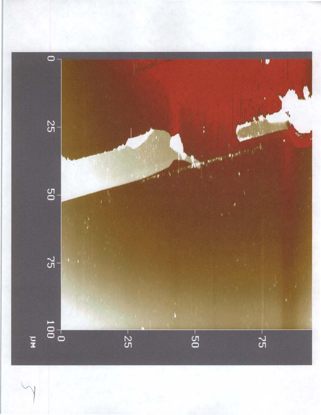
8 4 Results and Discussion Initially the deposition of gold, platinum, nickel, and cobalt was verified using the 10 mm solutions described earlier and potentials of approximately -1.0 to -1.5 V, with pulse durations of rnicroseconds and pulse frequencies on the order of 3 khz. The results obtained using nickel, of interest because of its use as a catalyst for nanotube growth, are of particular interest and are discussed in greater detail later on. While initial deposition attempts were successful in depositing metal onto the negative electrode, the deposition occurred all along the electrode in a nearly equal amount, as opposed to the desired goal of depositing only on the tip of the electrode axially towards the opposing (ground) electrode. An example of this type of deposition is given in figure 2. Several possible reasons for this were explored. First was the possibility that the connection between the macrostructure and microelectrodes was not complete for one of the electrodes. If, for instance, the circuit between the negative wire and negative electrode was not connected all the way out to the tip of the electrode the electric field generated by the voltage source would extend from the area of the disconnect to the ground electrode. Ideally this electric field should extend axially from the tip of one electrode to the tip of another. It was found to be possible to measure the impedance of the connection between the connecting wire and the macrostructure directly beside the microelectrode using a multimeter and a small wire. Using this measurement it was then possible to determine whether or not
9 5 the bulk connection was faulty, with an impedance (including some contact loss due to poor measuring wire connection) of between ohms expected for an intact half-circuit (from one wire to a corresponding gold pad right before the microelectrode). Inspection with the AFM could then be used to verify that the actual microelectrode structure was intact and not suffering from a gross defect (see Figure 3). Using these techniques several macro-structural defects created during initial fabrication or during post-lithographic handling were found, and, when possible, repaired with a conductive silver liquid. Although inspecting the macro- and micro- structures carefully for defect helped to insure that no gross connection failure was causing irregular deposition, even structures verified to be intact in every way still exhibited deposition all along the electrode, although usually in greater amount at the tip of the electrode. One possible explanation for this behavior was that deposition of material at the gap quickly depleted the surrounding solution of metal ions, resulting in a deficit of ions in the vicinity of the gap. Therefore deposition all along the electrode could occur in order to equalize the charge building up on it. To account for this effect pulse times were shortened to 5-20 microseconds and pulse frequencies moved to Hz. As seen in Figures 4 and 5 these modifications resulted in deposition occurring primarily at the tip of the electrode but still also somewhat on the sides and top of the electrode. In addition to this problem, it was also noticed that as many consecutive experiments were performed with the NiCI 2 solution the ground electrode was being depleted (see Tables 1 and 2 and Figures 6,7, and 8).
10 6 One possible explanation is that the voltage source was not perfectly grounded. Even a slightly positive potential occurring at the 'ground' terminal could have, over a long period of time (in comparison with the very short timeframe for negative potential application), caused gradual depletion of the ground electrode. This was easily corrected by simply grounding the voltage generator's 'ground' terminal to a true earth ground. One consequence of this depletion is that as experiments were performed to determine the optimum settings for the voltage source to maximize the precision of the deposition the ground electrode was being slowly depleted, changing the characteristics of the electric field between the two electrodes. Experiments to verify that this depletion problem has been solved by grounding the voltage source are still ongoing. When the 10 mm NiCb solution was used to deposit nickel onto an electrode it was observed that almost immediately the deposited nickel was reabsorbed into solution. Figures 9 and 10 demonstrate this process. Typically within 30 seconds of the deposition of a similar amount as in Figure 9 all Ni would have dissolved away, leaving the electrode in essentially the same condition it was in pre-deposition. It was determined that the cause of this solid Ni instability in solution was due to the slightly acidic ph (about 6.85) of the solution. By changing the ph to approximately 9.9 using a buffer solution it was possible to get the Ni to remain stable after deposited on an electrode. Despite the eventual undesirability of having unstable nickel, it proved extremely useful experimentally because it allowed one to test voltage source settings or solution
11 7 concentrations repeatable using the same expensive-to-fabricate electrode structure.
12 8 Conclusion The deposition process definitely functions with a variety of metal ions, and can be shown to be fairly selectively on the tip of the electrodes, but the desired precision deposition on the tip of the electrode only has not been demonstrated so far. Some problems with the deposition setup and process have been found and presumadely corrected but further experimentation is needed to insure that with an intact and 'functional macrostructure, adequate time given for diffusion to occur between pulses, and grounding problems solved that reproducible deposition occurs only axially out from the tip of the negative electrode, not on the sides that has occurred previously_ Having shown that it is possible to deposit nickel, and, by nl0difying the ph of the solution make the nickel remain on the electrode, if precise deposition on the tip of the electrode could be achieved these electrodes could be used for one of the many potential applications for nanoelectrodes, nanotube growth.
13 9 Acknowledgements I would like to thank my mentor, Dr. James W. Lee, for giving me the opportunity to work on and learn from such an interesting project. Also special thanks go to Dr. Ida Lee and Dr. Thomas Thundat for providing valuable advice and expertise regarding AFM operation. Thanks also go to the Department of Energy funded ERULF and ORISE programs, without which none of this would have been possible.
14 10 References 1Lee, J. W., and Greenbaum, E. Patent Application, 1999, No : Programmable Nanometer-Scale Electrolytic Deposition and Depletion.
15 11 Figures Figure 1: Overall geometry of the microelectrodes and connecting gold structure
16 Figure 2: Initial Deposition Attempt (using 10 mm Pt(NH3)4CI2) 12
17 Figure 3: Defective microelectrode. Gap approximately 20 microns across 13
18 Figure 4: Pre-deposition condition of device #6 14
19 Figure 5: Deposition of Ni in 10 mm NiCI 2 using microsecond pulses at 1 KHz (Device #6) 15
20 Figure 6: Pre-experiment condition of device #4 16
21 Figure 7: Condition of device #4 after multiple deposition and dissolution of Ni (top electrode negative, bottom electrode ground) 17

22 Figure 8: Condition of device #6 after multiple deposition and dissolution of Ni (top electrode negative, bottom electrode positive) 18
23 Figure 9: Massive Ni deposition onto device #2 (20, microsecond pulses at -1.SV) Time = 0 seconds 19
24 Figure 10: Device 2 at Time = 10 seconds 20
25 ! 21 Tables I I Ground Electrode Depletion Device 4 Negative Electrode Height [pre-deposition (nm) post-deposition (nm) Difference (nm) % Diff I % i % i % i % % % % % % % STDEV % MEAN % 95% Conf % Ground Electrode Height pre-deposition (nm) Ipost-deposition {nm' Difference (nm \ % Diff % % % % % % % % % % STDEV % MEAN % 95% Conf % Table 1: Change in height of ground and negative electrodes (deposition on negative, depletion on ground) for device #4
26 I 22 I Ground Electrode Depletion Device 6 Negative Electrode Height pre-deposition (nm) post-deposition (nm) Difference (nm) % Diff % % % % % % % % % % STDEV % MEAN % 95% Conf % Ground Electrode Height pre-deposition (nm) post-deposition (nm) Difference (nm) % Diff % % % % % % % % % % STDEV % MEAN % 95% Conf % Table 2: Change in height of ground and negative electrodes (deposition on negative, depletion on ground) for device #6
27
28
29
30
31
32
33
34
35

36

37
38

39
40

41 ,Concept.. ""'It... l""j~~"'''~~x~..:_,;;;.~:;.~-f'.'~:ii~~~>:~~j "I, :,,t.(~; 'l; ~:".' A set of gold electrodes is fabricated on a silicon oxide substrate using electron-beam lithography and vapor deposition with an initial distance between electrodes of approximately 1 micron. While under a metal-containing electrolyte solution such as NiCI 2, a potential is applied between the electrodes, setting up a strongly localized electric field between the tips of the electrodes. If a negative potential is used, deposition will occur only on the tip of the negative terminal as electrons are donated to the Pt ion in solution, likewise a positive potential results in depletion at the positive terminal.
42

43

44 1Jresentel to Kent Wilcher 9n 1f.(1(1recfafion {or 1/our Con{ri6u{fom as r.ne'j!j 1<tsearch l1ntle'jratfuate.t.a6orafo"!j ~e{fowshif1 Parficif1ant Chemical Technology Division Oak Ridge National Laboratory* *Managed by UT -Battelle, LLC, for the U.S. Dept. of Energy under contract DE-AC05-000R2272S. 7/ze"j 01 Date ( I 7 r. fj? CJ1.fl- Q 5 ~ L. E. McNeese, Director Chemical Technology Division

45 ORNL DWG Carbon Nanotube
46
.")
47 Applications Controllable nanotube placement at specific sites by deposition of Nickel, a catalyst for nanotuoe growth. NA sequencing (LDRD proposal already suomitted). olecular applications.

48 Electrolytic N anofab Chemical Technology Division Kent Wilcher Mentor: Dr. James Lee
49

50 erimental Set An Atomic Force Microscope (AFM) was used to monitor the deposition process in real... tim...,. U se of an AFM liquid cell allows scanning while under ionic solutions. he programmable voltage source used was caoable of changing the duration, magnitude, and time between pulses.
51

52
53
54

55 ORNL DWG 99C-44S Iding Through Ele ulsing Electrolytic Me Bypassing Circuit cted --E-""ition +: ~rogrgmmable Pul~ing Current Source yo,ass R
Design and Fabrication of a Capacitance Dilatometer for use in the Quantum Design Physical Property Measurement System
 University of Tennessee, Knoxville Trace: Tennessee Research and Creative Exchange University of Tennessee Honors Thesis Projects University of Tennessee Honors Program Spring 5-2002 Design and Fabrication
LaserTrim Ceramic Chip Capacitor
 DESCRIPTION Laser adjustable monolithic ceramic Rated voltage - 50V Porcelain Capacitors Excellent post-trim Q and ESR No capacitance drift APPLICATIONS Pagers, RF Modems Cellular Communications Remote
LaserTrim Ceramic Chip Capacitor
 DESCRIPTION Laser adjustable monolithic ceramic Rated voltage - 50V Porcelain Capacitors Excellent post-trim Q and ESR No capacitance drift APPLICATIONS Pagers, RF Modems Cellular Communications Remote
NTEGRA for EC PRESENTATION
 NTEGRA for EC PRESENTATION Application Purpose: In-situ control/modification of the surface morphology of single crystal and polycrystal electrodes (samples) during electrochemical process (in situ) in
CTAB-Influenced Electrochemical Dissolution of Silver Dendrites
 Supporting Information CTAB-Influenced Electrochemical Dissolution of Silver Dendrites Colm O Regan, 1, 2, 3 Xi Zhu, 4 Jun Zhong, 1, 2 Utkarsh Anand, 1, 2, 3, 5 Jingyu Lu, 1, 2, 3, 5 Haibin Su, 4 and 1,
REPORT ON SCANNING TUNNELING MICROSCOPE. Course ME-228 Materials and Structural Property Correlations Course Instructor Prof. M. S.
 REPORT ON SCANNING TUNNELING MICROSCOPE Course ME-228 Materials and Structural Property Correlations Course Instructor Prof. M. S. Bobji Submitted by Ankush Kumar Jaiswal (09371) Abhay Nandan (09301) Sunil
There's Plenty of Room at the Bottom
 There's Plenty of Room at the Bottom 12/29/1959 Feynman asked why not put the entire Encyclopedia Britannica (24 volumes) on a pin head (requires atomic scale recording). He proposed to use electron microscope
Nanotechnology Fabrication Methods.
 Nanotechnology Fabrication Methods. 10 / 05 / 2016 1 Summary: 1.Introduction to Nanotechnology:...3 2.Nanotechnology Fabrication Methods:...5 2.1.Top-down Methods:...7 2.2.Bottom-up Methods:...16 3.Conclusions:...19
ORION NanoFab: An Overview of Applications. White Paper
 ORION NanoFab: An Overview of Applications White Paper ORION NanoFab: An Overview of Applications Author: Dr. Bipin Singh Carl Zeiss NTS, LLC, USA Date: September 2012 Introduction With the advancement
Final Reading Assignment: Travels to the Nanoworld: pages pages pages
 Final Reading Assignment: Travels to the Nanoworld: pages 152-164 pages 201-214 pages 219-227 Bottom-up nanofabrication Can we assemble nanomachines manually? What are the components (parts)? nanoparticles
Kavli Workshop for Journalists. June 13th, CNF Cleanroom Activities
 Kavli Workshop for Journalists June 13th, 2007 CNF Cleanroom Activities Seeing nm-sized Objects with an SEM Lab experience: Scanning Electron Microscopy Equipment: Zeiss Supra 55VP Scanning electron microscopes
Instrumentation and Operation
 Instrumentation and Operation 1 STM Instrumentation COMPONENTS sharp metal tip scanning system and control electronics feedback electronics (keeps tunneling current constant) image processing system data
Topic: APPLIED ELECTROCHEMISTRY. Q.1 What is polarization? Explain the various type of polarization.
 Topic: APPLIED ELECTROCHEMISTRY T.Y.B.Sc Q.1 What is polarization? Explain the various type of polarization. Ans. The phenomenon of reverse e.m.f. brought about by the presence of product of electrolysis
Measuring charge transport through molecules
 Measuring charge transport through molecules utline Indirect methods 1. ptical techniques 2. Electrochemical techniques Direct methods 1. Scanning probe techniques 2. In-plane electrodes 3. Break junctions
Lecture 4. Conductance sensors. ChemFET. Electrochemical Impedance Spectroscopy. py Practical consideration for electrochemical biosensors.
 Lecture 4 Conductance sensors. ChemFET. Electrochemical Impedance Spectroscopy. py Practical consideration for electrochemical biosensors. Conductivity I V = I R=, L - conductance L= κa/, l Λ= κ /[ C]
e - Galvanic Cell 1. Voltage Sources 1.1 Polymer Electrolyte Membrane (PEM) Fuel Cell
 Fuel Cell") Galvanic cells convert different forms of energy (chemical fuel, sunlight, mechanical pressure, etc.) into electrical energy and heat. In this lecture, we are interested in some examples of galvanic cells.
Galvanic cells convert different forms of energy (chemical fuel, sunlight, mechanical pressure, etc.) into electrical energy and heat. In this lecture, we are interested in some examples of galvanic cells.
Chapter 10. Nanometrology. Oxford University Press All rights reserved.
 Chapter 10 Nanometrology Oxford University Press 2013. All rights reserved. 1 Introduction Nanometrology is the science of measurement at the nanoscale level. Figure illustrates where nanoscale stands
Thin Film Bi-based Perovskites for High Energy Density Capacitor Applications
 ..SKELETON.. Thin Film Bi-based Perovskites for High Energy Density Capacitor Applications Colin Shear Advisor: Dr. Brady Gibbons 2010 Table of Contents Chapter 1 Introduction... 1 1.1 Motivation and Objective...
Supplementary Materials
 Atomic layer-deposited tunnel oxide stabilizes silicon photoanodes for water oxidation Yi Wei Chen 1, Jonathan D. Prange 2, Simon Dühnen 2, Yohan Park 1, Marika Gunji 1, Christopher E. D. Chidsey 2, and
Chapter 24. Electrogravimetry and Coulometry
 Chapter 24 Electrogravimetry and Coulometry Dynamic Electrochemical Methods of analysis Electrolysis Electrogravimetric and Coulometric Methods For a cell to do any useful work or for an electrolysis to
MIL-STD-883E METHOD THERMAL CHARACTERISTICS
 THERMAL CHARACTERISTICS 1. PURPOSE. The purpose of this test is to determine the thermal characteristics of microelectronic devices. This includes junction temperature, thermal resistance, case and mounting
Institute for Electron Microscopy and Nanoanalysis Graz Centre for Electron Microscopy
 Institute for Electron Microscopy and Nanoanalysis Graz Centre for Electron Microscopy Micromechanics Ass.Prof. Priv.-Doz. DI Dr. Harald Plank a,b a Institute of Electron Microscopy and Nanoanalysis, Graz
NANONICS IMAGING FOUNTAIN PEN
 NANONICS IMAGING FOUNTAIN PEN NanoLithography Systems Methods of Nanochemical Lithography Fountain Pen NanoLithography A. Lewis et al. Appl. Phys. Lett. 75, 2689 (1999) FPN controlled etching of chrome.
Bio-electrochemistry Prof. Mainak Das Department of Biological Sciences & Bioengineering & Design Programme Indian Institute of Technology, Kanpur
 Bio-electrochemistry Prof. Mainak Das Department of Biological Sciences & Bioengineering & Design Programme Indian Institute of Technology, Kanpur Lecture 04 Galvanic Cells-I Welcome back to the lecture
UNIT 3. By: Ajay Kumar Gautam Asst. Prof. Dev Bhoomi Institute of Technology & Engineering, Dehradun
 UNIT 3 By: Ajay Kumar Gautam Asst. Prof. Dev Bhoomi Institute of Technology & Engineering, Dehradun 1 Syllabus Lithography: photolithography and pattern transfer, Optical and non optical lithography, electron,
Electrochemical Deposition of Carbon Nanotubes from Organic Solutions
 University of Central Florida UCF Patents Patent Electrochemical Deposition of Carbon Nanotubes from Organic Solutions 7-6-2004 Lee Chow University of Central Florida Elvira Anoshkina University of Central
A LAZAR LABORATORY HANDBOOK MEASUREMENT OF NITRIC OXIDE IN BIOLOGICAL SAMPLES
 A LAZAR LABORATORY HANDBOOK MEASUREMENT OF NITRIC OXIDE IN BIOLOGICAL SAMPLES Copyright Lazar Research Laboratories, Inc. 2004-1 - QUESTIONS? Call us at 1-800-824-2066 (1-323-931-1204 international), fax
SECTION #1 - The experimental setup
 Lemon Battery Connected in Series Charging a 2.2 Farad Capacitor SECTION #1 - The experimental setup 1. The goal of this experiment is to see if I can connect 2, 3 or 4 lemons together in a series configuration
Highly efficient hydrogen evolution of platinum via tuning the interfacial dissolved-gas concentration
 Electronic Supplementary Material (ESI) for Chemical Communications. This journal is The Royal Society of Chemistry 2018 Supporting Information for Highly efficient hydrogen evolution of platinum via tuning
SUPPLEMENTARY INFORMATION
 Ultrahigh interlayer friction in multiwalled boron nitride nanotubes 1 Contents Nanotubes production and characterizations 2 Experimental Methods 4 Post mortem characterization of the nanotubes 4 Références
Scanning Tunneling Microscopy Studies of the Ge(111) Surface
 Surface") VC Scanning Tunneling Microscopy Studies of the Ge(111) Surface Anna Rosen University of California, Berkeley Advisor: Dr. Shirley Chiang University of California, Davis August 24, 2007 Abstract: This
VC Scanning Tunneling Microscopy Studies of the Ge(111) Surface Anna Rosen University of California, Berkeley Advisor: Dr. Shirley Chiang University of California, Davis August 24, 2007 Abstract: This
some things to think about when doing evaporation liftoff of nanometer scale patterns 1/30/09
 some things to think about when doing evaporation liftoff of nanometer scale patterns 1/30/09 review fundamentals sample sample holder r dep = deposition rate (thickness/sec) r evap = evaporation rate
CHM 2046 Test #4 Review: Chapter 17 & Chapter 18
 1. Which of the following is true concerning a nonspontaneous reaction? a. It s impossible for the reaction to occur b. The reaction occurs, but very slowly c. It can be made spontaneous by adding a catalyst
Supporting Information
 Electronic Supplementary Material (ESI) for Nanoscale. This journal is The Royal Society of Chemistry 2014 Engineering Cu 2 O/NiO/Cu 2 MoS 4 Hybrid Photocathode for H 2 Generation in Water Chen Yang, a,b
Supplementary Figure 1 a) Scheme of microfluidic device fabrication by photo and soft lithography,
 Scheme of microfluidic device fabrication by photo and soft lithography,") a b 1 mm Supplementary Figure 1 a) Scheme of microfluidic device fabrication by photo and soft lithography, (a1, a2) 50nm Pd evaporated on Si wafer with 100 nm Si 2 insulating layer and 5nm Cr as an adhesion
a b 1 mm Supplementary Figure 1 a) Scheme of microfluidic device fabrication by photo and soft lithography, (a1, a2) 50nm Pd evaporated on Si wafer with 100 nm Si 2 insulating layer and 5nm Cr as an adhesion
Chapter 12. Nanometrology. Oxford University Press All rights reserved.
 Chapter 12 Nanometrology Introduction Nanometrology is the science of measurement at the nanoscale level. Figure illustrates where nanoscale stands in relation to a meter and sub divisions of meter. Nanometrology
CITY UNIVERSITY OF HONG KONG. Theoretical Study of Electronic and Electrical Properties of Silicon Nanowires
 CITY UNIVERSITY OF HONG KONG Ë Theoretical Study of Electronic and Electrical Properties of Silicon Nanowires u Ä öä ªqk u{ Submitted to Department of Physics and Materials Science gkö y in Partial Fulfillment
Multilayer Ceramic Chip Capacitors
 HIGH VOLTAGE SERIES JARO high voltage series Multilayer Ceramic Capacitors are constructed by depositing alternative layers of ceramic dielectric materials and internal metallic electrodes, by using advanced
What are Carbon Nanotubes? What are they good for? Why are we interested in them?
 Growth and Properties of Multiwalled Carbon Nanotubes What are Carbon Nanotubes? What are they good for? Why are we interested in them? - Interconnects of the future? - our vision Where do we stand - our
What is the importance of redox reactions? Their importance lies in the fact that we can use the transfer of electrons between species to do useful
 What is the importance of redox reactions? Their importance lies in the fact that we can use the transfer of electrons between species to do useful work. This is accomplished by constructing a voltaic
MAS.836 PROBLEM SET THREE
 MAS.836 PROBLEM SET THREE FSR, Strain Gauge, and Piezo Circuits: The purpose of this problem set is to familiarize yourself with the most common forms of pressure and force measurement. The circuits you
Analysis of cations and anions by Ion- Selective Electrodes (ISEs)
") Analysis of cations and anions by Ion- Selective Electrodes (ISEs) Purpose: The purpose of this assignment is to introduce potentiometric measurements of ionic species by ion selective electrodes (ISEs)
Analysis of cations and anions by Ion- Selective Electrodes (ISEs) Purpose: The purpose of this assignment is to introduce potentiometric measurements of ionic species by ion selective electrodes (ISEs)
Electrical Characterization with SPM Application Modules
 Electrical Characterization with SPM Application Modules Metrology, Characterization, Failure Analysis: Data Storage Magnetoresistive (MR) read-write heads Semiconductor Transistors Interconnect Ferroelectric
Unit 12 Conduction in Liquids and Gases
 Conduction in Liquids and Gases Objectives: Define positive and negative ions. Discuss electrical conduction in gases. Discuss electrical conduction in a liquid. Discuss several of the ionization processes.
Lithium-ion Batteries Based on Vertically-Aligned Carbon Nanotubes and Ionic Liquid
 Electronic Supplementary Information Lithium-ion Batteries Based on Vertically-Aligned Carbon Nanotubes and Ionic Liquid Electrolytes Wen Lu, * Adam Goering, Liangti Qu, and Liming Dai * 1. Synthesis of
1. Narrative Overview Questions
 Homework 4 Due Nov. 16, 010 Required Reading: Text and Lecture Slides on Downloadable from Course WEB site: http://courses.washington.edu/overney/nme498.html 1. Narrative Overview Questions Question 1
THERMAL CHARACTERIZATION OF MULTI-WALL CARBON NANOTUBE BUNDLES BASED ON PULSED LASER-ASSISTED THERMAL RELAXATION
 Functional Materials Letters Vol. 1, No. 1 (2008) 71 76 c World Scientific Publishing Company THERMAL CHARACTERIZATION OF MULTI-WALL CARBON NANOTUBE BUNDLES BASED ON PULSED LASER-ASSISTED THERMAL RELAXATION
RTAC104 AFM References in Package
 Radiant Technologies, Inc. 2835D Pan American Freeway NE Albuquerque, NM 87107 Tel: 505-842-8007 Fax: 505-842-0366 e-mail: radiant@ferrodevices.com www.ferrodevices.com RTAC104 AFM References in Package
ANALYSIS OF INDUCTIVE CURRENT PULSE DYNAMICS IN WATER ELECTROLYSES CELL
 ANALYSIS OF INDUCTIVE CURRENT PULSE DYNAMICS IN WATER ELECTROLYSES CELL Martins Vanags, Janis Kleperis, Gunars Bajars, Andrejs Lusis Institute of Solid State Physics of University of Latvia, Riga, LV-10050,
ANALYSIS OF LEAD IN SEAWATER
 ANALYSIS OF LEAD IN SEAWATER BY DIFFERENTIAL PULSE POLAROGRAPHY Introduction Electrochemical methods of analysis can be used for the quantitative analysis of any electroactive species any species that
Chemistry Instrumental Analysis Lecture 37. Chem 4631
 Chemistry 4631 Instrumental Analysis Lecture 37 Most analytes separated by HPLC are thermally stable and non-volatile (liquids) (unlike in GC) so not ionized easily by EI or CI techniques. MS must be at
CSCI 2570 Introduction to Nanocomputing
 CSCI 2570 Introduction to Nanocomputing The Emergence of Nanotechnology John E Savage Purpose of the Course The end of Moore s Law is in sight. Researchers are now exploring replacements for standard methods
GHZ ELECTRICAL PROPERTIES OF CARBON NANOTUBES ON SILICON DIOXIDE MICRO BRIDGES
 GHZ ELECTRICAL PROPERTIES OF CARBON NANOTUBES ON SILICON DIOXIDE MICRO BRIDGES SHENG F. YEN 1, HAROON LAIS 1, ZHEN YU 1, SHENGDONG LI 1, WILLIAM C. TANG 1,2, AND PETER J. BURKE 1,2 1 Electrical Engineering
Transient Thermal Measurement and Behavior of Integrated Circuits
 Transient Thermal Measurement and Behavior of Integrated Circuits Dustin Kendig¹*, Kazuaki Kazawa 1,2, and Ali Shakouri 2 ¹Microsanj LLC 3287 Kifer Rd, Santa Clara, CA 95051, USA ² Birck Nanotechnology
Supporting Information
 Supporting Information Universal, In-Situ Transformation of Bulky Compounds into Nanoscale Catalysts by High Temperature Pulse Shaomao Xu 1, (a), Yanan Chen 1, (a), Yiju Li 1, (a), Aijiang Lu 1, Yonggang
Characterisation of Nanoparticle Structure by High Resolution Electron Microscopy
 Journal of Physics: Conference Series OPEN ACCESS Characterisation of Nanoparticle Structure by High Resolution Electron Microscopy To cite this article: Robert D Boyd et al 2014 J. Phys.: Conf. Ser. 522
In-situ Imaging electrochemistry reaction with atomic force microscope and 3D desktop manufacturing in developing electrochemistry cells
 In-situ Imaging electrochemistry reaction with atomic force microscope and 3D desktop manufacturing in developing electrochemistry cells Song Xu, Ph.D. Sr. Application Scientist Agilent Technologies Why
Dominance of Old End Growth is Inherited in Fission Yeast
 University of Tennessee, Knoxville Trace: Tennessee Research and Creative Exchange University of Tennessee Honors Thesis Projects University of Tennessee Honors Program 5-2015 Dominance of Old End Growth
R. Ludwig and G. Bogdanov RF Circuit Design: Theory and Applications 2 nd edition. Figures for Chapter 6
 R. Ludwig and G. Bogdanov RF Circuit Design: Theory and Applications 2 nd edition Figures for Chapter 6 Free electron Conduction band Hole W g W C Forbidden Band or Bandgap W V Electron energy Hole Valence
Zn+2 (aq) + Cu (s) Oxidation: An atom, ion, or molecule releases electrons and is oxidized. The oxidation number of the atom oxidized increases.
 + Cu (s) Oxidation: An atom, ion, or molecule releases electrons and is oxidized. The oxidation number of the atom oxidized increases.") Oxidation-Reduction Page 1 The transfer of an electron from one compound to another results in the oxidation of the electron donor and the reduction of the electron acceptor. Loss of electrons (oxidation)
Oxidation-Reduction Page 1 The transfer of an electron from one compound to another results in the oxidation of the electron donor and the reduction of the electron acceptor. Loss of electrons (oxidation)
University of Maryland Department of Physics. Spring 2009 Final Exam 20. May (175 points) Post grades on web? (Initial, please) Yes No
 Post grades on web? (Initial, please) Yes No") University of Maryland Department of Physics Physics 122 20. May 2009 (175 points) Post grades on web? (Initial, please) Yes No (If you agree, I will post your grades and your detailed scores for each
University of Maryland Department of Physics Physics 122 20. May 2009 (175 points) Post grades on web? (Initial, please) Yes No (If you agree, I will post your grades and your detailed scores for each
EE301 RESISTANCE AND OHM S LAW
 Learning Objectives a. Describe the concept of resistance b. Use Ohm s law to calculate current, voltage, and resistance values in a circuit c. Discuss the difference between an open circuit and a short
PT/NI COUNTER-ELECTRODES WITH IMPROVED STABILITY FOR DYE SENSITIZED SOLAR CELLS
 PT/NI COUNTER-ELECTRODES WITH IMPROVED STABILITY FOR DYE SENSITIZED SOLAR CELLS G. Syrrokostas, G. Leftheriotis and P. Yianoulis Energy and Environment Lab, Physics Department, University of Patras, Rion,
11.3. Electrolytic Cells. Electrolysis of Molten Salts. 524 MHR Unit 5 Electrochemistry
 11.3 Electrolytic Cells Section Preview/ Specific Expectations In this section, you will identify the components of an electrolytic cell, and describe how they work describe electrolytic cells using oxidation
Structural and Mechanical Properties of Nanostructures
 Master s in nanoscience Nanostructural properties Mechanical properties Structural and Mechanical Properties of Nanostructures Prof. Angel Rubio Dr. Letizia Chiodo Dpto. Fisica de Materiales, Facultad
A NEW APPROACH TOWARDS PROPERTY NANOMEASUREMENTS USING IN-SITU TEM
 A NEW APPROACH TOWARDS PROPERTY NANOMEASUREMENTS USING IN-SITU TEM Z.L. WANG*, P. PONCHARAL**, W.A. DE HEER** and R.P. GAO* * School of Materials Science and Engineering, ** School of Physics, Georgia
Vapor-Phase Cutting of Carbon Nanotubes Using a Nanomanipulator Platform
 Vapor-Phase Cutting of Carbon Nanotubes Using a Nanomanipulator Platform MS&T 10, October 18, 2010 Vladimir Mancevski, President and CTO, Xidex Corporation Philip D. Rack, Professor, The University of
Supplementary information for
 Supplementary information for Transverse electric field dragging of DNA in a nanochannel Makusu Tsutsui, Yuhui He, Masayuki Furuhashi, Rahong Sakon, Masateru Taniguchi & Tomoji Kawai The Supplementary
Nanotechnology Nanofabrication of Functional Materials. Marin Alexe Max Planck Institute of Microstructure Physics, Halle - Germany
 Nanotechnology Nanofabrication of Functional Materials Marin Alexe Max Planck Institute of Microstructure Physics, Halle - Germany Contents Part I History and background to nanotechnology Nanoworld Nanoelectronics
Introduction to Nanotechnology Chapter 5 Carbon Nanostructures Lecture 1
 Introduction to Nanotechnology Chapter 5 Carbon Nanostructures Lecture 1 ChiiDong Chen Institute of Physics, Academia Sinica chiidong@phys.sinica.edu.tw 02 27896766 Carbon contains 6 electrons: (1s) 2,
Università degli Studi di Bari "Aldo Moro"
 Università degli Studi di Bari "Aldo Moro" Table of contents 1. Introduction to Atomic Force Microscopy; 2. Introduction to Raman Spectroscopy; 3. The need for a hybrid technique Raman AFM microscopy;
Fundamentals of the Metal Oxide Semiconductor Field-Effect Transistor
 Triode Working FET Fundamentals of the Metal Oxide Semiconductor Field-Effect Transistor The characteristics of energy bands as a function of applied voltage. Surface inversion. The expression for the
Bridge between research in modern physics and entrepreneurship in nanotechnology. Quantum Physics
 Bridge between research in modern physics and entrepreneurship in nanotechnology Quantum Physics The physics of the very small with great applications Part 2 QUANTUM PROPERTIES & TECHNOLOGY TRANSLATION
Basic overall reaction for hydrogen powering
 Fuel Cell Basics Basic overall reaction for hydrogen powering 2H 2 + O 2 2H 2 O Hydrogen produces electrons, protons, heat and water PEMFC Anode reaction: H 2 2H + + 2e Cathode reaction: (½)O 2 + 2H +
GRAPHENE ON THE Si-FACE OF SILICON CARBIDE USER MANUAL
 GRAPHENE ON THE Si-FACE OF SILICON CARBIDE USER MANUAL 1. INTRODUCTION Silicon Carbide (SiC) is a wide band gap semiconductor that exists in different polytypes. The substrate used for the fabrication
Magnon-drag thermopile
 Magnon-drag thermopile I. DEVICE FABRICATION AND CHARACTERIZATION Our devices consist of a large number of pairs of permalloy (NiFe) wires (30 nm wide, 20 nm thick and 5 µm long) connected in a zigzag
Fuel Cells Activation polarization
 Fuel Cells The principle of fuel cells Oxygen and hydrogen, when mixed together in the presence of enough activation energy have a natural tendency to react and form water, because the Gibbs free energy
Carbonized Electrospun Nanofiber Sheets for Thermophones
 Supporting Information Carbonized Electrospun Nanofiber Sheets for Thermophones Ali E. Aliev 1 *, Sahila Perananthan 2, John P. Ferraris 1,2 1 A. G. MacDiarmid NanoTech Institute, University of Texas at
1 Written and composed by: Prof. Muhammad Ali Malik (M. Phil. Physics), Govt. Degree College, Naushera
, Govt. Degree College, Naushera") CURRENT ELECTRICITY Q # 1. What do you know about electric current? Ans. Electric Current The amount of electric charge that flows through a cross section of a conductor per unit time is known as electric
CURRENT ELECTRICITY Q # 1. What do you know about electric current? Ans. Electric Current The amount of electric charge that flows through a cross section of a conductor per unit time is known as electric
Nanolithography Techniques
 Nanolithography Techniques MSE 505 / MSNT 505 P. Coane Outline What Is Nanotechnology? The Motivation For Going Small Nanofabrication Technologies Basic Techniques Nano Lithography NANOTECHNOLOGY Nanotechnology
Self-study problems and questions Processing and Device Technology, FFF110/FYSD13
 Self-study problems and questions Processing and Device Technology, FFF110/FYSD13 Version 2016_01 In addition to the problems discussed at the seminars and at the lectures, you can use this set of problems
Supplemental Information. Carbon Monoxide Gas Diffusion Electrolysis. that Produces Concentrated C 2 Products. with High Single-Pass Conversion
 JOUL, Volume 3 Supplemental Information Carbon Monoxide Gas Diffusion Electrolysis that Produces Concentrated C 2 Products with High Single-Pass Conversion Donald S. Ripatti, Thomas R. Veltman, and Matthew
Instructors Guide: Introduction to Voltaic Cells
 Instructors Guide: Introduction to Voltaic Cells Standards Connections: Connections to NSTA Standards for Science Teacher Preparation C.3.a.8 Oxidation reduction chemistry. Connections to the National
The molecules that will be studied with this device will have an overall charge of
 The Basics of the Rotation of Polarized Light The molecules that will be studied with this device will have an overall charge of zero but will have localized polarities that can be used to orient the molecule.
Electro - Principles I
 Electro - Principles I Page 10-1 Atomic Theory It is necessary to know what goes on at the atomic level of a semiconductor so the characteristics of the semiconductor can be understood. In many cases a
Nickel Phosphide-embedded Graphene as Counter Electrode for. Dye-sensitized Solar Cells **
 Nickel Phosphide-embedded Graphene as Counter Electrode for Dye-sensitized Solar Cells ** Y. Y. Dou, G. R. Li, J. Song, and X. P. Gao =.78 D 1359 G 163 a =.87 D 138 G 159 b =1.3 D 1351 G 1597 c 1 15 1
High Performance, Low Operating Voltage n-type Organic Field Effect Transistor Based on Inorganic-Organic Bilayer Dielectric System
 Journal of Physics: Conference Series PAPER OPEN ACCESS High Performance, Low Operating Voltage n-type Organic Field Effect Transistor Based on Inorganic-Organic Bilayer Dielectric System To cite this
Sensors, Signals and Noise 1 COURSE OUTLINE. Introduction Signals and Noise Filtering Sensors: Strain Gauges. Signal Recovery, 2017/2018 Strain Gauges
 Sensors, Signals and Noise 1 COURSE OUTLINE Introduction Signals and Noise Filtering Sensors: Strain Gauges Strain Gauges 2 Stress and strain in elastic materials Piezoresistive Effect Strain Gauge principle
Fat: Who Says? Measuring Obesity by Bioelectrical Impedance Analysis
 Fat: Who Says? Measuring Obesity by Bioelectrical Impedance Analysis Circuitous Adventures Activity 3C Part 2 Objectives: Using simple electrical components, students will be able to: Identify a simple
OAKRIDGE _ NATIONALLABORATORY
 d OAKRIDGE _ NATIONALLABORATORY MANAGED BY UT-BAlTELLE FOR THE DEPARTMENT OF ENERGY CIORNL96-0398 CRADA for CRADA Number ORNL96-0398 MOISTURE SENSOR FOR SULFUR NEXAFLUORDE (SF6)-FILLED CIRCUIT BREAKERS
The Mechanism of Electropolishing of Nb in Hydrofluoric-Sulfuric Acid (HF+H 2 SO 4 ) Electrolyte
 Electrolyte") The Mechanism of Electropolishing of Nb in Hydrofluoric-Sulfuric Acid (HF+H 2 SO 4 ) Electrolyte Hui Tian *+, Charles E. Reece +, Michael J. Kelley *+ Applied Science Department, College of William and
The Mechanism of Electropolishing of Nb in Hydrofluoric-Sulfuric Acid (HF+H 2 SO 4 ) Electrolyte Hui Tian *+, Charles E. Reece +, Michael J. Kelley *+ Applied Science Department, College of William and
Nova 600 NanoLab Dual beam Focused Ion Beam IITKanpur
 Nova 600 NanoLab Dual beam Focused Ion Beam system @ IITKanpur Dual Beam Nova 600 Nano Lab From FEI company (Dual Beam = SEM + FIB) SEM: The Electron Beam for SEM Field Emission Electron Gun Energy : 500
DE '! N0V ?
 "7 CONF-851174 24 DE86 004682 '! N0V26 1985? PREDICTION OF FLOW RATES THROUGH AN ORIFICE AT PRESSURES CORRESPONDING TO THE TRANSITION BETWEEN MOLECULAR AND ISENTROPIC FLOW S. F. DeMuth Fuel Recycle Division
Final exam: take-home part
 Final exam: take-home part! List five things that can be done to improve this class. Be specific; give much detail.! (You will be penalized only for insulting comments made for no benefit; you will not
Supporting Information. Electropolymerization of aniline on nickel-based electrocatalysts substantially
 Supporting Information Electropolymerization of aniline on nickel-based electrocatalysts substantially enhances their performance for hydrogen evolution Fuzhan Song, Wei Li, Guanqun Han, and Yujie Sun*
The Low Temperature Physics of Thin Films Superconducting Tin and Monolayer Graphene
 The Low Temperature Physics of Thin Films Superconducting Tin and Monolayer Graphene Abstract: The aim of this project was to investigate how the electrical resistance of a conductor changes if it is deposited
Experiment 28 DIRECT METHANOL FUEL CELL
 Experiment 28 Direct methanol fuel cell 1 Experiment 28 DIRECT METHANOL FUEL CELL Objective The purpose of this experiment is to learn the principle of direct methanol fuel cell (DMFC) and set up a simple
Supporting Information. Three-Dimensional Super-Resolution Imaging of Single Nanoparticle Delivered by Pipettes
 Supporting Information Three-Dimensional Super-Resolution Imaging of Single Nanoparticle Delivered by Pipettes Yun Yu,, Vignesh Sundaresan,, Sabyasachi Bandyopadhyay, Yulun Zhang, Martin A. Edwards, Kim
Chapter 3 Engineering Science for Microsystems Design and Fabrication
 Lectures on MEMS and MICROSYSTEMS DESIGN and MANUFACTURE Chapter 3 Engineering Science for Microsystems Design and Fabrication In this Chapter, we will present overviews of the principles of physical and
VI. EIS STUDIES LEAD NANOPOWDER
 VI. EIS STUDIES LEAD NANOPOWDER 74 26. EIS Studies of Pb nanospheres Impedance (valid for both DC and AC), a complex resistance occurs when current flows through a circuit (composed of various resistors,