Physics of Nanotubes, Graphite and Graphene Mildred Dresselhaus
|
|
|
- Emil Stewart
- 5 years ago
- Views:
Transcription


1 Quantum Transport and Dynamics in Nanostructures The 4 th Windsor Summer School on Condensed Matter Theory 6-18 August 2007, Great Park Windsor (UK) Physics of Nanotubes, Graphite and Graphene Mildred Dresselhaus Massachusetts Institute of Technology, Cambridge, MA
2 Physics of Nanotubes, Graphite and Graphene Outline of Lecture 1 - Nanotubes Brief overview of carbon nanotubes Review of Photophysics of Nanotubes Phonon assisted Photoluminescence Double wall carbon nanotubes Nano-Metrology
3 Carbon Nanotube researchstill a growing field 1991 nanotube observation by Sumio Iijima (NEC) opening field number of publications is still growing exponentially number of publications containing Carbon Nanotube vs. time Iijima, S., Helical Microtubules of Graphitic Carbon. Nature, (6348): p


 Zigzag")
")

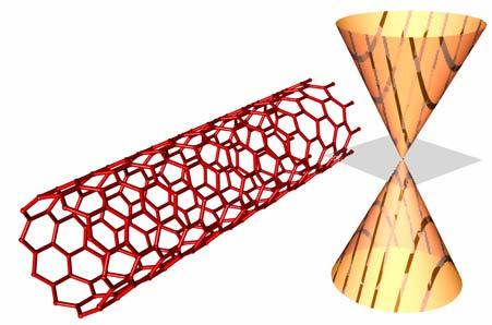
4 Carbon Nanotubes (5,5) Armchair Nanotube (9,0) Zigzag Nanotube (6,5) Chiral Nanotube (n,m) notation focuses on symmetry of cylinder edge


5 Carbon materials Diamond Graphite (hexagonal, rhombohedral) HOPG (highly oriented pyrolytic graphite) Pyrolytic graphite Turbostratic graphite Kish graphite Liquid carbon Amorphous carbon Carbon and graphitic foams Carbon fibers Fullerenes Nanotubes Nanohorns Graphene fibers and scrolls Graphene Graphene ribbons

")
 1855 cm -1")

6 3D, 2D, 1D Carbon Materials Diamond sp 3 (3D) 1332 cm -1 Graphite sp 2 (2D) 1582 cm -1 Chain sp 1 (1D) 1855 cm -1 All are Raman active with characteristic frequencies


7 Unique Properties of Carbon Nanotubes within the Nanoworld graphene sheet SWNT armchair zigzag chiral Size: Nanostructures with dimensions of ~1 nm diameter (~10 atoms around the cylinder) Electronic Properties: Can be either metallic or semiconducting depending on diameter and orientation of the hexagons Mechanical: Very high strength, modulus, and resiliency. Good properties on both compression and extension. Physics: 1D density of electronic states Single molecule Raman spectroscopy and luminescence. Single molecule transport properties. Heat pipe, electromagnetic waveguide.


8 One Dimensional Systems: High aspect ratio Enhanced density of states Single wall carbon nanotubes SWNT: Nanowire Chirality and diameter-dependent properties Nanotube D. O. S. D. O. S. D. O. S. D. O. S. E E E E 3D Bulk Semiconductor 2D Quantum Well 1D Quantum Wire 0D Quantum Dot
 h = 1 + 2 θ = L a dt = = n + nm + m π π 1 3m tan 2n + m 2 2 Each (n,m) nanotube is a unique molecule R.")
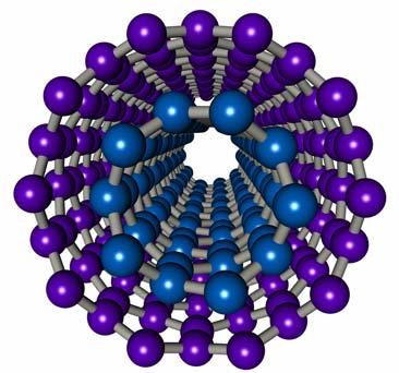
9 Nanotube Structure in a Nutshell (4,2) Graphene Sheet SWNT Rolled-up graphene layer Large unit cell. C na ma ( n, m) h = θ = L a dt = = n + nm + m π π 1 3m tan 2n + m 2 2 Each (n,m) nanotube is a unique molecule R.Saito et al, Imperial College Press, 1998


10 Electronic structure of a carbon nanotube Rolling up 2D graphene sheet Confinement of 1D electronic states 1D van Hove singularities - high density of electronic states (DOS) at well defined energies Graphene ribbons resemble nanotubes in some ways
11 Metal or Semiconductor? R. Saito et al., Appl. Phys. Lett. 60, 2204 (1992) Density of States Depending on Chirality, Diameter 3p n m = 3 p ± 1 metal semiconductor E gap 1/ d t Each (n,m) nanotube is a unique molecule Armchair graphene ribbons can be M or S
12 Physics of Nanotubes, Graphite and Graphene Outline of Lecture 1 - Nanotubes Brief overview of carbon nanotubes Review of Photophysics of Nanotubes Phonon assisted Photoluminescence Double wall carbon nanotubes Nano-Metrology

13 Resonance Raman Spectroscopy (RRS) A.M. Rao et al., Science 275 (1997) 187 RRS: R.C.C. Leite & S.P.S. Porto, PRL 17, (1966) Enhanced Signal Raman spectra from SWNT bundles Optical Absorption e-dos peaks E = 0.94eV = 1.17eV π π diameter-selective resonance process ω RBM = α /d t = 1.58eV = 1.92eV = 2.41eV
 G-band resonant Raman spectra laser energy G-band Diameter dependence of the Van-Hove")
14 Resonant Raman Spectra of Carbon Nanotube Bundles M. A. Pimenta (UFMG) et al., Phys. Rev. B 58, R16016 (1998) G-band resonant Raman spectra laser energy G-band Diameter dependence of the Van-Hove singularities d t = 1.37 ± 0.18 nm

 Semiconducting Metallic ' Each nanotube has a unique DOS")

15 RBM Single Nanotube Spectroscopy yields E ii, (n,m( n,m) Resonant Raman spectra for isolated single-wall carbon nanotubes grown on Si/SiO 2 substrate by the CVD method A. Jorio (UFMG) et al., Phys. Rev. Lett. 86, 1118 (2001) Semiconducting Metallic ' Each nanotube has a unique DOS because of trigonal warping effects Raman signal from one SWNT indicates a strong resonance process R. Saito et al., Phys. Rev. B 61, 2981 (2000) (ω RBM, E ii ) (n,m)
16 Raman Spectra of SWNT Bundles G-band Metallic G-band G - G + G + Raman Intensity RBM: ω RBM 1/d t G - D-band G + G -band o Raman Shift (cm 1 ) RBM gives tube diameter and diameter distribution Raman D-band characterizes structural disorder G - band distinguished M, S tubes and G + relates to charge transfer G band (2nd order of D-band) provides connection of phonon to its wave vector

 2361.")
![Energy [ev] 2 c 1 c 2 1.](/docs-images/82/86357397/images/17-2.jpg "2 g/cm 3 SDS=Sodium Dodecyl Sulfate 0 fluorescence")
 2 0 Density of Electronic States e-dos")
17 Water, 1.1 g/cm 3 SDS 1.0 g/cm 3 Band Gap Fluorescence M. J. O Connell O et al., Science 297 (2002) 593 S. M. Bachilo et al., Science 298 (2002) Energy [ev] 2 c 1 c g/cm 3 SDS=Sodium Dodecyl Sulfate 0 fluorescence absorption v 1 v 2 Excitation (nm) Peaks only Emission (nm) 2 0 Density of Electronic States e-dos of (n, m) = (10,5) Initially (n,m) assignments were made by empirical excitation-emission pattern
 2n+m=constant family patterns are observed in the PL")

18 PHOTOLUMINESCENCE SDS-wrapped HiPco nanotubes in solution S. M. Bachilo et al., Science 298, 2361 (2002) 2n+m=constant family patterns are observed in the PL excitation-emission spectra Identification of ratio problem Showed value of mapping optical transitions Perhaps this technique can be applied to study graphene ribbons
19 Raman Mapping of a Nanotube 1600cm -1 x RBM 173cm cm x (µm) (µm) (µm) (µm) (µm) -10 H. Son et al. unpublished (2006) (µm)
 et al.")
 stb γ 0 =2.")
20 Resonance Raman Spectroscopy on the same sample used for PL E 33 S E 11 M E 22 S RRS 2n+m = constant family behavior is observed E 33 S Fantini (UFMG) et al. PRL (2004) showed RRS and PL give the same E ii Family effects are mainly due to trigonal warping E 11 M E 22 S simple tight binding (stb) stb γ 0 =2.9eV The simple TB does not describe E ii correctly!
 geometrical structure optimization The extended tight-binding calculations show family behavior (differentiation between S1 & S2 and strong chirality dependence)")
21 EXTENDED TIGHT BINDING MODEL Kataura plot is calculated within the extended tight-binding approximation using Popov/Porezag approach: Transition Energy (ev) curvature effects (ssσ, spσ, ppσ, ppπ) long-range interactions (up to ~4Å) geometrical structure optimization The extended tight-binding calculations show family behavior (differentiation between S1 & S2 and strong chirality dependence) similar to that of the PL empirical fit Inverse Diameter (1/nm) M 2n+m=3p S1 2n+m=3p+1 S2 2n+m=3p+2 Family behavior is strongly influenced by the trigonal warping effect Ge.G. Samsonidze et al., APL 85, 5703 (2004) N.V. Popov et al Nano Lett. 4, 1795 (2004) & New J. Phys. 6, 17 (2004)

 = type I 0 : metal 1 : type I SC 2 :")
, (7,2), (6,4)")
22 Brillouin zone (BZ) 2D graphene BZ 2n+m families in SWNTs R. Saito et al., Phys. Rev. B, 72, (2005) SWNT BZ K K Family mod (2n+m, 3) = type I 0 : metal 1 : type I SC 2 : type II SC type II (example) 2n+m = const family type I type II separation (8,0), (7,2), (6,4) 2n+m = 16 type I family
23 Physics of Nanotubes, Graphite and Graphene Outline of Lecture 1 - Nanotubes Brief overview of carbon nanotubes Review of Photophysics of Nanotubes Phonon assisted Photoluminescence Double wall carbon nanotubes Nano-Metrology
 species M. Zheng, et al. Science 302, 1546 (2003) Average DNA helical pitch ~ 11nm, height ~ 1.08nm.")
24 DNA wrapping of SWNTs DNA Wrapping: provides good separation of CoMoCAT SWNT sample Subsequent fractionation: results in sample strongly enriched in (6,5) species M. Zheng, et al. Science 302, 1546 (2003) Average DNA helical pitch ~ 11nm, height ~ 1.08nm.
 SWNTs Chromatography further removes M SWNTs")
25 DNA-Assisted Assisted SEPARATION M. Zheng et al., Science, 302,1546 (2003). column containing stationary phase load sample add eluant collect samples Raman characterization shows that DNA wrapping removes metallic (M) SWNTs Chromatography further removes M SWNTs preferentially Ion-exchange chromatography (IEC) Hybrid DNA-SWNTs: M-SWNT different surface charge density, higher polarizability, elute before S-CNTs RBM Spectra Taken at E laser = 2.18eV CoMoCAT CNT (No DNA) DNA-CNT M (6,5) S Fractionated DNA-CNT Raman Shift (cm -1 )
 identifications.")

26 Nanotube PL Spectroscopy Most Measurements - excitation at E 22, emission at E 11 - measured with Xe lamp - (2n+m) family patterns provide (n, m) identifications. Our Measurements (6,5) enriched sample Intense light source (laser) Allows observation of phonon assisted processes PL map of SDS- dispersed HiPco CNTs Maruyama et al. NJP (2003) Maruyama s work suggests study of detailed phonon-assisted excitonic relaxation processes for different phonon branches.
27 PL Spectra of (6,5) Nanotubes Excitation Energy (ev) Emission Energy (ev) 1.3 Phonon-assisted transitions on an expanded scale Chou, et al PRL 94, (2005) E11 = 1.26eV E22 = 2.18eV
28 Excitons in Carbon Nanotubes Experimental Justification for excitons 2-photon excitation to a 2A + symmetry exciton (2p) and 1-photon emission from a 1A exciton (1s) cannot be explained by the free electron model 1A E 11 (1s) 2A+ E 11 (2p) BAND-EDGE ABSORPTION (a.u.) PHOTON EXCITATION ENERGY The observation that excitation and emission are at different frequencies supports exciton model 1A E 11 (1s) EMISSION ENERGY 1.4 (9,1) (8,3) 1.3 (6,5) (7,5) 1.2` PHOTON EXCITATION ENERGY Wang et al. Science 308, 838 (2005)
 et al, PRL 95, 247401 (2005) E 11 S -E 11 S Perebeinos, Tersoff and Avouris, PRL 94, 027402")
29 The exciton-phonon sidebands further support exciton model HiPco + SDS solution E 22 S -E 11 S Sideband F. Plentz Filho (UFMG) et al, PRL 95, (2005) E 11 S -E 11 S Perebeinos, Tersoff and Avouris, PRL 94, (2005)
 1iLO/iTO near Γ (G-band) Chou et al.")
30 Emission Identified with One and Two Phonon Processes: 2 ilo/ito near Γ Phonon dispersion relations of graphite 2 ito near K (G band) 2 ilo/ila near K 2 oto near Γ(M-band) 1iLO/iTO near Γ (G-band) Chou et al., PRL 94, (2005) Two phonon process One phonon process
31 Non-degenerate Pump-probe probe Frequency domain S. G. Chou et al. PRL (2005) Fast optics, Time domain E pump = 1.57±0.01eV, ~E 11 (6,5)+2ħω D E probe = around E 11 of (6,5) nanotube (Instrument resolution ~250fs) E Pump ~E 11(6,5) + 2ħω ph, D Eprobe =E 11(6,5) Pump Intraband relaxation Probe Interband relaxation S. G. Chou et al. Phys. Rev. B (2005)
32 Pump Probe Studies at Special E pump E pump = 1.57±0.01eV E 11 1A- (6,5) +2ħω D E probe = around E 11 1Aof (6,5) nanotube Intraband relaxation Pump Probe at band edge Exciton population at E 11 1A- (6,5): Quick rise (within 200fs) Three decay components: τ fast ~680fs (dominant process) τ int ~2-3ps (dominant process) τ slow ~50ps (weak during first 20ps). K
33 Exp. (n,m) E Probe FluenceJ/m 2 fast % Int % Slow % O 5 (8,3) 1.27eV fs 70 Several ps Traces mixed 30ps 30 O 4 (6,5) 1.25eV fs 45 3ps 45 50ps 10 O 2 (7,5) 1.20eV fs 90 N/A N/A 40ps 10 Probing at Different Energies: -Pump at 1.57±0.01 ev 1.27eV(8,3) E ii j E 1A- 11 E 1A- 11 (6, 1A- (8,3) + 2hw D 6,5) + 2hw D 1.25eV(6,5) u E 11 1A- (7,5) + 2hw D 1A- (7 1.22eV 1.20eV(7,5) 1.16eV o 5 o 4 o 3 o 2 o 1 E 11 1A- E 11 1A- 1A- (6 E 11 1A- 1A- (8.3) (6,5) (7,5) 1A- (7 z 0 K


34 Why? More on Excitons Large binding energy (0.5eV) Even at room temperature, excitons exist. Exciton specific phenomena dark excitons, two photon, environment What can we know or imagine? Near cancellation by self energy ETB + many body effects reproduce Eii Localized exciton wave function enhancement of optical process Length dependence. Wang et al. Science 308, 838 (2005) 2+ A 1-11 (2p) A 11 (1s)


35 Exciton exists only in the 3M-triangle E11S E22S E55S E44S E33S Energy minima for the π band exist only in 3MΔ. Cutting lines occur around K-point.
36 Centre of mass motion Symmetry considerations J. Jiang et al. Phys. Rev. B (2007) :Good quantum number Relative motion A symmetry excitons Bright and dark excitons A - : bright exciton A +, E and E *: dark excitons K K Γ K e h K e h C Γ 2 K Γ e hk K A ±
37 E symmetry exciton and its dispersion E exciton h K E* exciton K K e K K e K K K h Bright and dark excitons A - : bright exciton A +, E, E *: dark excitons Dispersion for (6,5) NT
38 Lowest energy but not symmetry allowed Dark state has the lowest energy J. Jiang et al. Phys. Rev. B (2007) A - : bright exciton A - : bright exciton A +, E and E *: dark excitons
39 Physics of Nanotubes, Graphite and Graphene Outline of Lecture 1 - Nanotubes Brief overview of carbon nanotubes Review of Photophysics of Nanotubes Phonon assisted Photoluminescence Double wall carbon nanotubes Nano-Metrology
40 Raman Spectra of SWNT Bundles G-band Metallic G-band G - G + Raman Intensity RBM: ω RBM 1/d t G - D-band G + G -band o Raman Shift (cm 1 ) Photophysics of SWNTs is now at an advanced stage Photophysics of MWNTs (DWNTs) is at an early stage
41 Motivation for studying DWNTs Applications world shows much interest Synthesis world has made major progress Promising for fundamental physics Study of the interface between DWNTs and bilayer graphene should enrich both areas


42 Approaches to DWNTs simplest assumption + = Suggests using Kataura plots for SWNTs as first approximation for DWNTs, but E(k) of monolayer and bilayer graphene say more detail is needed

")
 Br 2 -DWNTs")


 5 nm")

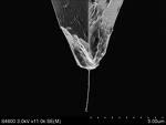
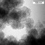
43 Br 2 -doped double-wall nanotubes TEM images (a) Pristine DWNTs (b) Br 2 -DWNTs Highly pure samples (99% of DWNTs + 1% of SWNTs + catalysts particles) 5 nm (c) 5 nm (d) SEM images 100nm 100nm Endo et al. Nanolett. 4,1451 (2004)
44 Kataura plot: undoped vs. doped SWNTs using Extended Tight Binding Model Outer tubes Inner tubes d t (nm) Doped (+0.04 e - /C) Undoped E ii (ev) E M 11 E S E S E S Different configurations for outer/inner nanotubes depending on laser energy Frequency (cm 1 )
45 Semiconducting outer/metallic inner configuration M S RBM properties at E laser =2.33 ev Breathing mode spectrum from the Br 2 dopant Resonance with Bromine electronic transitions Can identify individual (n,m) inner tubes from Kataura plot Raman Intensity (arb. units) 1.0 (a) E Laser = 2.33 ev (12,3) (11,5) (9,6) (7,7) Pristine (8,5) (9,3) Raman Intensity (arb. units) 1.4 (b) E laser = 2.33 ev Frequency (cm -1 ) A.Souza-Filho. et al PRB (2006) Br Br 2 -doped 2 Frequency (cm -1 ) Frequency (cm 1 )
46 Metallic outer/semiconducting inner configuration Raman Intensity (arb. units) 1.0 Raman Intensity (arb. units) Frequency (cm -1 ) 3 (a) 1.0 E laser = 1.58 ev (9,4) Frequency (cm -1 ) 39 S (10,2) 36 * M RBM properties at E laser =1.58 ev 29 * (11,0) pristine (9,1) E S 11 Intensity enhancement after bromine doping Doping changing relative intensities of (n,m) tubes The Kataura plot for SWNTs gives identification for inner wall tubes and shows doping effect (b) E laser = 1.58 ev Br 2 doped 1.4 (9,4) (10,2) Frequency (cm -1 ) * * (11,0) E S Frequency (cm 1 ) Frequency (cm -1 )
47 Metallic shielding effects Metallic outer/semiconducting inner wall D and G band (DWNTs) E laser =1.58 ev S M Raman Intensity Frequency (cm -1 ) 1301 Br 2 -doped D band 1554 Pristine Frequency (cm -1 ) The G-band is predominantly from semiconducting Nanotubes (based on diameter dependence) No shift in the G-band for semiconducting inner tubes The inner tubes are shielded by the metallic outer tubes
48 Charge transfer effects Semiconducting outer/metallic inner E laser =2.33 ev D and G band (DWNTs) Br 2 -doped M S Raman Intensity D band Frequency (cm -1 ) x0.5 Pristine Frequency (cm -1 ) Frequency (cm -1 ) The G-band profile is a mixing of semiconducting and metallic profiles; Shift in the G-band from semiconducting outer tubes indicates charge transfer to the Br 2 molecules The BWF (Breit Wigner Fano) decreases after doping. The decrease in the overall intensity indicates depletion of states
49 Charge transfer and screening effects Raman Intensity (a) M Br 2 doped Pristine S x0.3 Raman Intensity Frequency (cm -1 ) Metallic inner tubes highly affected by doping E laser 2.33 ev (b) G band Raman spectra of Br 2 doped DWNTs. S M E laser 1.58 ev Semiconducting inner tubes is not affected when shielded by metallic tubes Frequency (cm -1 )

50 Calculated electronic charge density difference (ρ doped - ρ undoped ) of DWNTs Calculation supports experimental observations about charge transfer A.G. Souza Filho et al Nano Letters (2007)
51 Outer tubes Undoping experiments on bromine doped DWNTs Br 2 -adsorbed DWNTs Br 2 Inner tubes E laser =2.33 ev Br 2 Energy needed for removing Br 2 is ~ 25 mev Raman Intensity cooling 21 o C heating 600 o C Frequency (cm -1 ) 21 o C The dopant is completely removed after heat treatment Souza Filho et al, PRB (2006)
52 Spectrum for RBM for pristine and H 2 SO 4 doped DWNTs Outer Walls M Inner Walls H 2 SO 4 doped E laser =2.052 ev Pristine Raman Intensity S Frequency (cm -1 ) Outer walls strongly affected by doping Inner semiconducting (S) tubes weakly interact with dopant Inner metallic (M) tubes more strongly interact with dopant E. Barros et al, PRB (2007)
53 What we learned from intercalation studies of DWNTs The Kataura plot from SWNTs provides a semi-quantitive interpretation of frequencies for inner wall tubes for DWNTs The M/S configuration shields inner semiconducting tubes from the effect of the dopant The S/M configuration allows charge transfer to inner metallic tubes S M M S This work potentially relates to bilayer graphene
54 Laser Energy Dependence of G -band Spectra The ~2450 cm -1 peak (TO+LA) in DWNTs is downshifted relative to the corresponding peak in SWNTs The SWNT G band corresponds to peak 3 of DWNTs Frequency (cm -1 ) SWNTs ev inner outer Frequency (cm -1 ) Excitation Energy (ev) Some resemblance to bilayer graphene E. B. Barros et al., PRB in press (2007)
55 Physics of Nanotubes, Graphite and Graphene Outline of Lecture 1 - Nanotubes Brief overview of carbon nanotubes Review of Photophysics of Nanotubes Phonon assisted Photoluminescence Double wall carbon nanotubes Nano-Metrology
56 The problem of Nano-metrology Why do we need metrology for nanotechnology? Why do we need reference standards? What is new about metrology at the nano-scale? What does nanoscience have to do with metrology? World wide production of Carbon Nanotubes MWNTs 270 tons/yr ( kg/year) SWNTs 7 tons/yr ( kg/year) 8K US$ / kg to US$ / kg (R. Blackmon,

57 Metrology is guided by applications Potential Applications of Carbon Nanotubes by M. Endo, M. S. Strano, P. M. Springer TAP111 Large Volume Applications Limited Volume Applications (Mostly based on Engineered Nanotube Structures) Present Near Term (less than ten years) Long Term (beyond ten years) - Battery Electrode Additives (MWNT) - Composites (sporting goods; MWNT) - Composites (ESD* applications; MWNT) *ESD Electrical Shielding Device - Battery and Super-capacitor Electrodes - Multifunctional Composites - Fuel Cell Electrodes (catalyst support) - Transparent Conducting Films - Field Emission Displays / Lighting - CNT based Inks for Printing - Power Transmission Cables - Structural Composites (aerospace and automobile etc.) - CNT in Photovoltaic Devices - Scanning Probe Tips (MWNT) - Specialized Medical Appliances (catheters) (MWNT) - Single Tip Electron Guns - Multi-Tip Array X-ray Sources - Probe Array Test Systems - CNT Brush Contacts - CNT Sensor Devices - Electro-mechanical Memory Device - Thermal Management Systems - Nano-electronics (FET,Interconnects) - Flexible Electronics - CNT based bio-sensors - CNT Fitration/Separation Membranes - Drug-delivery Systems
 100 90 80 70 60 50 40 30 20 10 0 Quality")
 ~mg Experiment Number 77.")
 Quartz cyrstal microbalance (QCM) Mass Remaining, % 100 90 80 70 60")
58 What should we measure? At which scale? Quantity vs. mass Mass remaining Remaining, % (%) Quality Statistical Comparison QCM shows SWNTs are non-homogeneous already at the μg scale TGA (375 C) ~mg Experiment Number % experiment number 25 mass remaining (%) Thermogravimetric analysis (TGA) Quartz cyrstal microbalance (QCM) Mass Remaining, % QCM (375 C) ~µg % experiment Experiment Number number 25


 IBM")

59 Can we trust the measurements? What do we use for measuring nanomaterials properties? 4-PROBES TRANSPORT 2 R 14 R 12 +R 23 +R SCANNING PROBES ELECTRON MICROSCOPY Purewal et al.,prl 98, (2007) IBM Website LIGHT: Raman and photoluminescence LOCALIZED LIGHT EMISSON 50nm From Achim Hartschuh From Hubert - FEI


60 Can we trust the measurements? What is the ideal environment? Encapsuled by micelles Suspended in air Sitting on a substrate Within a forest Nano-metrology is a wide open area for development requiring collaboration between metrology and nanoscience experts
Chirality and energy dependence of first and second order resonance Raman intensity
 NT06: 7 th International Conference on the Science and Application of Nanotubes, June 18-23, 2006 Nagano, JAPAN Chirality and energy dependence of first and second order resonance Raman intensity R. Saito
Why are we so excited about carbon nanostructures? Mildred Dresselhaus Massachusetts Institute of Technology Cambridge, MA
 Why are we so excited about carbon nanostructures? Mildred Dresselhaus Massachusetts Institute of Technology Cambridge, MA Conference for Undergraduate Women in Physics at Yale January 18, 2009 Why are
Carbon Nanomaterials
 Carbon Nanomaterials STM Image 7 nm AFM Image Fullerenes C 60 was established by mass spectrographic analysis by Kroto and Smalley in 1985 C 60 is called a buckminsterfullerene or buckyball due to resemblance
The Photophysics of Nano Carbons. Kavli Institute, UC Santa Barbara January 9, 2012 M. S. Dresselhaus, MIT
 The Photophysics of Nano Carbons Kavli Institute, UC Santa Barbara January 9, 2012 M. S. Dresselhaus, MIT The Electronic Structure of Graphene Near the K point E ( ) v F linear relation where and and 0
Physics of Nanotubes, Graphite and Graphene Mildred Dresselhaus
 Quantum Transport and Dynamics in Nanostructures The 4 th Windsor Summer School on Condensed Matter Theory 6-18 August 2007, Great Park Windsor (UK) Physics of Nanotubes, Graphite and Graphene Mildred
Carbon Nanotubes and Bismuth Nanowires
 1653_C03.fm Page 55 Friday, December 17, 2004 2:35 PM 3 Carbon Nanotubes and Bismuth Nanowires Milded. S. Dresselhaus, Ado Jorio, and Oded Rabin CONTENTS 3.1 Introduction...55 3.2 Carbon Nanotubes...56
The Kataura plot over broad energy and diameter ranges
 Early View publication on www.interscience.wiley.com (issue and page numbers not yet assigned; citable using Digital Object Identifier DOI) Original phys. stat. sol. (b), 1 5 (006) / DOI 10.100/pssb.0066919
Optical Spectroscopy of Single-Walled Carbon Nanotubes
 Optical Spectroscopy of Single-Walled Carbon Nanotubes Louis Brus Chemistry Department, Columbia University Groups: Heinz, O Brien, Hone, Turro, Friesner, Brus 1. SWNT Luminescence dynamics psec pump-probe
Electron Interactions and Nanotube Fluorescence Spectroscopy C.L. Kane & E.J. Mele
 Electron Interactions and Nanotube Fluorescence Spectroscopy C.L. Kane & E.J. Mele Large radius theory of optical transitions in semiconducting nanotubes derived from low energy theory of graphene Phys.
Calculating Electronic Structure of Different Carbon Nanotubes and its Affect on Band Gap
 Calculating Electronic Structure of Different Carbon Nanotubes and its Affect on Band Gap 1 Rashid Nizam, 2 S. Mahdi A. Rizvi, 3 Ameer Azam 1 Centre of Excellence in Material Science, Applied Physics AMU,
A.Jorio, M. A. Pimenta and P. T. Araujo. S. K. Doorn. S. Maruyama
 NT06: eventh International Conference on the cience and Application of Nanotubes June 18-23, 2006 Nature of Optical Transitions in Carbon Nanotubes and Population Analysis A.Jorio, M. A. Pimenta and P.
Metallic/semiconducting ratio of carbon nanotubes in a bundle prepared using CVD technique
 PRAMANA c Indian Academy of Sciences Vol. 67, No. 2 journal of August 2006 physics pp. 395 400 Metallic/semiconducting ratio of carbon nanotubes in a bundle prepared using CVD technique KHURSHED AHMAD
Hydrogen Storage in Single- and Multi-walled Carbon Nanotubes and Nanotube Bundles
 Australian Journal of Basic and Applied Sciences, 5(7): 483-490, 2011 ISSN 1991-8178 Hydrogen Storage in Single- and Multi-walled Carbon Nanotubes and Nanotube Bundles 1 S. Hamidi and 2 H. Golnabi 1 Physics
Introduction to Nanotechnology Chapter 5 Carbon Nanostructures Lecture 1
 Introduction to Nanotechnology Chapter 5 Carbon Nanostructures Lecture 1 ChiiDong Chen Institute of Physics, Academia Sinica chiidong@phys.sinica.edu.tw 02 27896766 Section 5.2.1 Nature of the Carbon Bond
Graphene and Carbon Nanotubes
 Graphene and Carbon Nanotubes 1 atom thick films of graphite atomic chicken wire Novoselov et al - Science 306, 666 (004) 100μm Geim s group at Manchester Novoselov et al - Nature 438, 197 (005) Kim-Stormer
Optical properties of nanotube bundles by photoluminescence excitation and absorption spectroscopy
 Physica E 40 (2008) 2352 2359 www.elsevier.com/locate/physe Optical properties of nanotube bundles by photoluminescence excitation and absorption spectroscopy P.H. Tan a,b,, T. Hasan a, F. Bonaccorso a,c,
status solidi Raman spectroscopy of ( n, m )-identified individual single-walled carbon nanotubes
-identified individual single-walled carbon nanotubes") physica pss status solidi basic solid state physics b Raman spectroscopy of ( n, m )-identified individual single-walled carbon nanotubes T. Michel 1, M. Paillet 1, J. C. Meyer 2, V. N. Popov 3, L. Henrard
physica pss status solidi basic solid state physics b Raman spectroscopy of ( n, m )-identified individual single-walled carbon nanotubes T. Michel 1, M. Paillet 1, J. C. Meyer 2, V. N. Popov 3, L. Henrard
Observation of charged excitons in hole-doped carbon nanotubes using photoluminescence and absorption spectroscopy
 Observation of charged excitons in hole-doped carbon nanotubes using photoluminescence and absorption spectroscopy Ryusuke Matsunaga 1, Kazunari Matsuda 1, and Yoshihiko Kanemitsu 1,2 1 Institute for Chemical
Determining Carbon Nanotube Properties from Raman. Scattering Measurements
 Determining Carbon Nanotube Properties from Raman Scattering Measurements Ying Geng 1, David Fang 2, and Lei Sun 3 1 2 3 The Institute of Optics, Electrical and Computer Engineering, Laboratory for Laser
2 Symmetry. 2.1 Structure of carbon nanotubes
 2 Symmetry Carbon nanotubes are hollow cylinders of graphite sheets. They can be viewed as single molecules, regarding their small size ( nm in diameter and µm length), or as quasi-one dimensional crystals
ACCVD Growth, Raman and Photoluminescence Spectroscopy of Isotopically Modified Single-Walled Carbon Nanotubes
 ACCVD Growth, Raman and Photoluminescence Spectroscopy of Isotopically Modified Single-Walled Carbon Nanotubes Shigeo Maruyama and Yuhei Miyauchi Department of Mechanical Engineering, The University of
Carbon Nanotubes (CNTs)
") Carbon Nanotubes (s) Seminar: Quantendynamik in mesoskopischen Systemen Florian Figge Fakultät für Physik Albert-Ludwigs-Universität Freiburg July 7th, 2010 F. Figge (University of Freiburg) Carbon Nanotubes
Carbon Nanotubes (s) Seminar: Quantendynamik in mesoskopischen Systemen Florian Figge Fakultät für Physik Albert-Ludwigs-Universität Freiburg July 7th, 2010 F. Figge (University of Freiburg) Carbon Nanotubes
Processing and Properties of Highly Enriched Double-Walled. Carbon Nanotubes: Supplementary Information
 Processing and Properties of Highly Enriched Double-Walled Carbon Nanotubes: Supplementary Information Alexander A. Green and Mark C. Hersam* Department of Materials Science and Engineering and Department
Transparent Electrode Applications
 Transparent Electrode Applications LCD Solar Cells Touch Screen Indium Tin Oxide (ITO) Zinc Oxide (ZnO) - High conductivity - High transparency - Resistant to environmental effects - Rare material (Indium)
Exciton Photophysics of Carbon Nanotubes
 Annu. Rev. Phys. Chem. 27.58:719-747. Downloaded from arjournals.annualreviews.org Annu. Rev. Phys. Chem. 27. 58:719 47 First published online as a Review in Advance on January 2, 27 The Annual Review
Lectures Graphene and
 Lectures 15-16 Graphene and carbon nanotubes Graphene is atomically thin crystal of carbon which is stronger than steel but flexible, is transparent for light, and conducts electricity (gapless semiconductor).
Raman spectroscopy study of heat-treated and boron-doped double wall carbon nanotubes
 Raman spectroscopy study of heat-treated and boron-doped double wall carbon nanotubes F. Villalpando-Paez, 1 H. on, 2. G. Chou, 3 Ge. G. amsonidze, 2 Y. A. Kim, 4 H. Muramatsu, 4 T. Hayashi, 4 M. Endo,
SUPPLEMENTARY INFORMATION
 SUPEMENTARY INFORMATION DOI:.38/NNANO.23.9 Bright, long-lived and coherent excitons in carbon nanotube quantum dots Matthias S. Hofmann, Jan T. Glückert, Jonathan Noé, Christian Bourjau, Raphael Dehmel,
Interaction between Single-walled Carbon Nanotubes and Water Molecules
 Workshop on Molecular Thermal Engineering Univ. of Tokyo 2013. 07. 05 Interaction between Single-walled Carbon Nanotubes and Water Molecules Shohei Chiashi Dept. of Mech. Eng., The Univ. of Tokyo, Japan
EXCITONS, PLASMONS, AND EXCITONIC COMPLEXES UNDER STRONG CONFINEMENT IN QUASI-1D SEMICONDUCTORS. Theory and Perspectives
 EXCITONS, PLASMONS, AND EXCITONIC COMPLEXES UNDER STRONG CONFINEMENT IN QUASI-1D SEMICONDUCTORS. Theory and Perspectives Igor Bondarev Math & Physics Department North Carolina Central University Durham,
Near-field imaging and spectroscopy of electronic states in single-walled carbon nanotubes
 Early View publication on www.interscience.wiley.com (issue and page numbers not yet assigned; citable using Digital Object Identifier DOI) Original phys. stat. sol. (b), 1 5 (2006) / DOI 10.1002/pssb.200669179
Identification of the constituents of double-walled carbon nanotubes using Raman spectra taken with different laser-excitation energies
 Identification of the constituents of double-walled carbon nanotubes using Raman spectra taken with different laser-excitation energies Feng Li Shenyang National Laboratory for Materials Science, Institute
In today s lecture, we will cover:
 In today s lecture, we will cover: Metal and Metal oxide Nanoparticles Semiconductor Nanocrystals Carbon Nanotubes 1 Week 2: Nanoparticles Goals for this section Develop an understanding of the physical
Tube tube interaction in double-wall carbon nanotubes
 phys. stat. sol. (b) 243, No. 13, 3268 3272 (2006) / DOI 10.1002/pssb.200669176 Tube tube interaction in double-wall carbon nanotubes R. Pfeiffer *, 1, F. Simon 1, 2, H. Kuzmany 1, V. N. Popov 3, V. Zólyomi
Intraband emission of GaN quantum dots at λ =1.5 μm via resonant Raman scattering
 Intraband emission of GaN quantum dots at λ =1.5 μm via resonant Raman scattering L. Nevou, F. H. Julien, M. Tchernycheva, J. Mangeney Institut d Electronique Fondamentale, UMR CNRS 8622, University Paris-Sud
SUPPLEMENTARY INFORMATION
 SUPPLEMENTARY INFORMATION Phonon populations and electrical power dissipation in carbon nanotube transistors Supplemental Information Mathias Steiner 1, Marcus Freitag 1, Vasili Perebeinos 1, James C.
Fig. 1: Raman spectra of graphite and graphene. N indicates the number of layers of graphene. Ref. [1]
![Fig. 1: Raman spectra of graphite and graphene. N indicates the number of layers of graphene. Ref. [1]](/thumbs/90/102653942.jpg "Fig. 1: Raman spectra of graphite and graphene. N indicates the number of layers of graphene. Ref. [1]") Vibrational Properties of Graphene and Nanotubes: The Radial Breathing and High Energy Modes Presented for the Selected Topics Seminar by Pierce Munnelly 09/06/11 Supervised by Sebastian Heeg Abstract
Vibrational Properties of Graphene and Nanotubes: The Radial Breathing and High Energy Modes Presented for the Selected Topics Seminar by Pierce Munnelly 09/06/11 Supervised by Sebastian Heeg Abstract
Low Dimensional System & Nanostructures Angel Rubio & Nerea Zabala. Carbon Nanotubes A New Era
 Low Dimensional System & Nanostructures Angel Rubio & Nerea Zabala Carbon Nanotubes A New Era By Afaf El-Sayed 2009 Outline World of Carbon - Graphite - Diamond - Fullerene Carbon Nanotubes CNTs - Discovery
Carbon nanotubes in a nutshell. Graphite band structure. What is a carbon nanotube? Start by considering graphite.
 Carbon nanotubes in a nutshell What is a carbon nanotube? Start by considering graphite. sp 2 bonded carbon. Each atom connected to 3 neighbors w/ 120 degree bond angles. Hybridized π bonding across whole
Raman study on single-walled carbon nanotubes with different laser excitation energies
 Bull. Mater. Sci., Vol. 30, No. 3, June 2007, pp. 295 299. Indian Academy of Sciences. Raman study on single-walled carbon nanotubes with different laser excitation energies S S ISLAM*, KHURSHED AHMAD
Carbon nanotubes in a nutshell
 Carbon nanotubes in a nutshell What is a carbon nanotube? Start by considering graphite. sp 2 bonded carbon. Each atom connected to 3 neighbors w/ 120 degree bond angles. Hybridized π bonding across whole
Carbon Nanotube: The Inside Story
 Krasnoyarsk: 24 th August, 2009 Carbon Nanotube: The Inside Story Review written for Journal of Nanoscience and Nanotechnology Yoshinori ANDO Dean of Faculty of Science and Technology, Meijo University
Direct Observation of Inner and Outer G Band Double-resonance Raman Scattering in Free Standing Graphene
 Direct Observation of Inner and Outer G Band Double-resonance Raman Scattering in Free Standing Graphene Zhiqiang Luo 1, Chunxiao Cong 1, Jun Zhang 1, Qihua Xiong 1 1, 2, 3*, Ting Yu 1. Division of Physics
Observation of exciton-phonon sideband in individual metallic single-walled carbon nanotubes
 Title Observation of exciton-phonon sideband in individual metallic single-walled carbon nanotubes Author(s) Zeng, H; Zhao, H; Zhang, FC; Cui, X Citation Physical Review Letters, 2009, v. 102 n. 13 Issued
Manifestation of Structure of Electron Bands in Double-Resonant Raman Spectra of Single-Walled Carbon Nanotubes
 Stubrov et al. Nanoscale Research Letters (2016) 11:2 DOI 10.1186/s11671-015-1213-8 NANO EXPRESS Manifestation of Structure of Electron Bands in Double-Resonant Raman Spectra of Single-Walled Carbon Nanotubes
Supplementary Information
 Emiss. Inten. (arb. unit) Emiss. Inten. (arb. unit) Supplementary Information Supplementary Figures S-S a b..5. c.2 d.2 (6,5) (7,5) (6,5).8 (7,6).8.6.4.2 (9,) (8,4) (9,4) (8,6) (,2).6.4.2 (7,5) (7,6)(8,4)
The calculation of energy gaps in small single-walled carbon nanotubes within a symmetry-adapted tight-binding model
 The calculation of energy gaps in small single-walled carbon nanotubes within a symmetry-adapted tight-binding model Yang Jie( ) a), Dong Quan-Li( ) a), Jiang Zhao-Tan( ) b), and Zhang Jie( ) a) a) Beijing
Second-order harmonic and combination modes in graphite, single wall carbon nanotube bundles, and isolated single wall carbon nanotubes
 Second-order harmonic and combination modes in graphite, single wall carbon nanotube bundles, and isolated single wall carbon nanotubes V. W. Brar a, Ge. G. Samsonidze b, M. S. Dresselhaus a,b, G. Dresselhaus
Spectroscopies for Unoccupied States = Electrons
 Spectroscopies for Unoccupied States = Electrons Photoemission 1 Hole Inverse Photoemission 1 Electron Tunneling Spectroscopy 1 Electron/Hole Emission 1 Hole Absorption Will be discussed with core levels
Band-like transport in highly crystalline graphene films from
 Supplementary figures Title: Band-like transport in highly crystalline graphene films from defective graphene oxides R. Negishi 1,*, M. Akabori 2, T. Ito 3, Y. Watanabe 4 and Y. Kobayashi 1 1 Department
Theory of Rayleigh scattering from metallic carbon nanotubes
 PHYSICAL REVIEW B 77, 5 8 Theory of Rayleigh scattering from metallic carbon nanotubes Ermin Malić,, * Matthias Hirtschulz, Frank Milde, Yang Wu, Janina Maultzsch, Tony F. Heinz, Andreas Knorr, and Stephanie
Manipulating and determining the electronic structure of carbon nanotubes
 Manipulating and determining the electronic structure of carbon nanotubes (06.12.2005 NTHU, Physics Department) Po-Wen Chiu Department of Electrical Engineering, Tsing Hua University, Hsinchu, Taiwan Max-Planck
CHARACTERISATION OF CARBON NANOTUBE MATERIALS BY RAMAN SPECTROSCOPY AND MICROSCOPY A CASE STUDY OF MULTIWALLED AND SINGLEWALLED SAMPLES
 Journal of Optoelectronics and Advanced Materials Vol. 6, No. 4, December 24, p. 1269-1274 CHARACTERISATION OF CARBON NANOTUBE MATERIALS BY RAMAN SPECTROSCOPY AND MICROSCOPY A CASE STUDY OF MULTIWALLED
Optical & Transport Properties of Carbon Nanotubes II
 Optical & Transport Properties of Carbon Nanotubes II Duncan J. Mowbray Nano-Bio Spectroscopy Group European Theoretical Spectroscopy Facility (ETSF) Donostia International Physics Center (DIPC) Universidad
2.2 Important Spectral and Polarized Properties of Semiconducting SWNT Photoluminescence
 2.2 Important Spectral and Polarized Properties of Semiconducting SWNT Photoluminescence Shigeo Maruyama and Yuhei Miyauchi 2.2.1 Important Spectral features Photoluminescence (PL) of single-walled carbon
Introduction to Nanotechnology Chapter 5 Carbon Nanostructures Lecture 1
 Introduction to Nanotechnology Chapter 5 Carbon Nanostructures Lecture 1 ChiiDong Chen Institute of Physics, Academia Sinica chiidong@phys.sinica.edu.tw 02 27896766 Carbon contains 6 electrons: (1s) 2,
The Pennsylvania State University. The Graduate School. Department of Physics OPTICAL PROPERTIES OF CARBON NANOTUBES. A Thesis in.
 The Pennsylvania State University The Graduate School Department of Physics OPTICAL PROPERTIES OF CARBON NANOTUBES A Thesis in Physics by Gugang Chen 2003 Gugang Chen Submitted in Partial Fulfillment of
Calculation of Cutting Lines of Single-Walled Carbon Nanotubes
 65 C.Ü. Fen Fakültesi Fen Bilimleri Dergisi, Cilt 33, No. 1 (2012) Calculation of Cutting Lines of Single-Walled Carbon Nanotubes Erdem UZUN 1* 1 Karamanoğlu Mehmetbey Üniversitesi, Fen Fakültesi, Fizik
Carbon Nanomaterials: Nanotubes and Nanobuds and Graphene towards new products 2030
 Carbon Nanomaterials: Nanotubes and Nanobuds and Graphene towards new products 2030 Prof. Dr. Esko I. Kauppinen Helsinki University of Technology (TKK) Espoo, Finland Forecast Seminar February 13, 2009
Electrical and Optical Properties. H.Hofmann
 Introduction to Nanomaterials Electrical and Optical Properties H.Hofmann Electrical Properties Ohm: G= σw/l where is the length of the conductor, measured in meters [m], A is the cross-section area of
FMM, 15 th Feb Simon Zihlmann
 FMM, 15 th Feb. 2013 Simon Zihlmann Outline Motivation Basics about graphene lattice and edges Introduction to Raman spectroscopy Scattering at the edge Polarization dependence Thermal rearrangement of
ELECTRONIC ENERGY DISPERSION AND STRUCTURAL PROPERTIES ON GRAPHENE AND CARBON NANOTUBES
 ELECTRONIC ENERGY DISPERSION AND STRUCTURAL PROPERTIES ON GRAPHENE AND CARBON NANOTUBES D. RACOLTA, C. ANDRONACHE, D. TODORAN, R. TODORAN Technical University of Cluj Napoca, North University Center of
SUPPLEMENTARY INFORMATION
 SUPPLEMENTARY INFORMATION Facile Synthesis of High Quality Graphene Nanoribbons Liying Jiao, Xinran Wang, Georgi Diankov, Hailiang Wang & Hongjie Dai* Supplementary Information 1. Photograph of graphene
Curvature-induced optical phonon frequency shift in metallic carbon nanotubes
 Curvature-induced optical phonon frequency shift in metallic carbon nanotubes Ken-ichi Sasaki, 1 Riichiro Saito, 1 Gene Dresselhaus, 2 Mildred S. Dresselhaus, 3,4 Hootan Farhat, 5 and Jing Kong 4 1 Department
Seminars in Nanosystems - I
 Seminars in Nanosystems - I Winter Semester 2011/2012 Dr. Emanuela Margapoti Emanuela.Margapoti@wsi.tum.de Dr. Gregor Koblmüller Gregor.Koblmueller@wsi.tum.de Seminar Room at ZNN 1 floor Topics of the
For more information, please contact: or +1 (302)
") Introduction Graphene Raman Analyzer: Carbon Nanomaterials Characterization Dawn Yang and Kristen Frano B&W Tek Carbon nanomaterials constitute a variety of carbon allotropes including graphene, graphene
Introduction Graphene Raman Analyzer: Carbon Nanomaterials Characterization Dawn Yang and Kristen Frano B&W Tek Carbon nanomaterials constitute a variety of carbon allotropes including graphene, graphene
Control of Diameter Distribution of Single-walled Carbon Nanotubes Using the Zeolite-CCVD Method
 22 Special Issue Nano-structure Controls of Functional Powders Research Report Control of Diameter Distribution of Single-walled Carbon Nanotubes Using the Zeolite-CCVD Method Atsuto Okamoto, Hisanori
Supplementary Figure 1. Selected area electron diffraction (SAED) of bilayer graphene and tblg. (a) AB
 of bilayer graphene and tblg. (a) AB") Supplementary Figure 1. Selected area electron diffraction (SAED) of bilayer graphene and tblg. (a) AB stacked bilayer graphene (b), (c), (d), (e), and (f) are twisted bilayer graphene with twist angle
Supplementary Figure 1. Selected area electron diffraction (SAED) of bilayer graphene and tblg. (a) AB stacked bilayer graphene (b), (c), (d), (e), and (f) are twisted bilayer graphene with twist angle
Double resonance Raman study of disorder in CVD-grown single-walled carbon nanotubes. Talapatra, 3 Benji Maruyama 1
 Double resonance Raman study of disorder in CVD-grown single-walled carbon nanotubes Rahul Rao, 1* Jason Reppert, 2 Xianfeng Zhang, 3 Ramakrishna Podila, 2 Apparao M. Rao, 2 Saikat Talapatra, 3 Benji Maruyama
Outline. What we learned at NT08; Achievements and Trends Reports from satellite meetings Challenges & Future Work
 Outline Jean Christophe Charlier Ado Jorio E. Flauhaut Jing Kong Mario Hofmann Mildred S. Dresselhaus What we learned at NT08; Achievements and Trends Reports from satellite meetings Challenges & Future
Environmental effects on photoluminescence of single-walled carbon nanotubes
 Chapter X Environmental effects on photoluminescence of single-walled carbon nanotubes Yutaka Ohno, Shigeo Maruyama *, and Takashi Mizutani Department of Quantum Engineering, Nagoya University * Department
CHAPTER 6 CHIRALITY AND SIZE EFFECT IN SINGLE WALLED CARBON NANOTUBES
 10 CHAPTER 6 CHIRALITY AND SIZE EFFECT IN SINGLE WALLED CARBON NANOTUBES 6.1 PREAMBLE Lot of research work is in progress to investigate the properties of CNTs for possible technological applications.
7. Carbon Nanotubes. 1. Overview: Global status market price 2. Types. 3. Properties. 4. Synthesis. MWNT / SWNT zig-zag / armchair / chiral
 7. Carbon Nanotubes 1. Overview: Global status market price 2. Types MWNT / SWNT zig-zag / armchair / chiral 3. Properties electrical others 4. Synthesis arc discharge / laser ablation / CVD 5. Applications
Title: Ultrafast photocurrent measurement of the escape time of electrons and holes from
 Title: Ultrafast photocurrent measurement of the escape time of electrons and holes from carbon nanotube PN junction photodiodes Authors: Nathaniel. M. Gabor 1,*, Zhaohui Zhong 2, Ken Bosnick 3, Paul L.
GeSi Quantum Dot Superlattices
 GeSi Quantum Dot Superlattices ECE440 Nanoelectronics Zheng Yang Department of Electrical & Computer Engineering University of Illinois at Chicago Nanostructures & Dimensionality Bulk Quantum Walls Quantum
physical Carbon Nanotubes Properties of Physical Properties of Carbon Nanotubes Downloaded from
 physical Properties of Carbon Nanotubes This page is intentionally left blank Rysical Properties of Carbon Nanotubes GDRESSELElAUS & M S DRBSELMUS MZT Imperial College Press Published by Imperial College
Imaging Carbon materials with correlative Raman-SEM microscopy. Introduction. Raman, SEM and FIB within one chamber. Diamond.
 Imaging Carbon materials with correlative Raman-SEM microscopy Application Example Carbon materials are widely used in many industries for their exceptional properties. Electric conductance, light weight,
In the name of Allah
 In the name of Allah Nano chemistry- 4 th stage Lecture No. 1 History of nanotechnology 16-10-2016 Assistance prof. Dr. Luma Majeed Ahmed lumamajeed2013@gmail.com, luma.ahmed@uokerbala.edu.iq Nano chemistry-4
We are IntechOpen, the first native scientific publisher of Open Access books. International authors and editors. Our authors are among the TOP 1%
 We are IntechOpen, the first native scientific publisher of Open Access books 3,350 108,000 1.7 M Open access books available International authors and editors Downloads Our authors are among the 151 Countries
University of Louisville - Department of Chemistry, Louisville, KY; 2. University of Louisville Conn Center for renewable energy, Louisville, KY; 3
 Ultrafast transient absorption spectroscopy investigations of charge carrier dynamics of methyl ammonium lead bromide (CH 3 NH 3 PbBr 3 ) perovskite nanostructures Hamzeh Telfah 1 ; Abdelqader Jamhawi
Chirality-dependent G-band Raman intensity of carbon nanotubes
 PHYSICAL REVIEW B, VOLUME 64, 085312 Chirality-dependent G-band Raman intensity of carbon nanotubes R. Saito, 1 A. Jorio, 2 J. H. Hafner, 3 C. M. Lieber, 3 M. Hunter, 4 T. McClure, 5 G. Dresselhaus, 6
status solidi Department of Biological Physics, Eötvös University, Pázmány Péter sétány 1/A, 1117 Budapest, Hungary 2
 physica pss www.pss-b.com status solidi basic solid state physics b Curvature effects in the D * band of small diameter carbon nanotubes J. Kürti,V. Zólyomi,,J. Koltai, F. Simon 3, 4,R. Pfeiffer 4, and
Carbon Nanotubes in Interconnect Applications
 Carbon Nanotubes in Interconnect Applications Page 1 What are Carbon Nanotubes? What are they good for? Why are we interested in them? - Interconnects of the future? Comparison of electrical properties
CVD growth of Graphene. SPE ACCE presentation Carter Kittrell James M. Tour group September 9 to 11, 2014
 CVD growth of Graphene SPE ACCE presentation Carter Kittrell James M. Tour group September 9 to 11, 2014 Graphene zigzag armchair History 1500: Pencil-Is it made of lead? 1789: Graphite 1987: The first
Quantized Electrical Conductance of Carbon nanotubes(cnts)
") Quantized Electrical Conductance of Carbon nanotubes(cnts) By Boxiao Chen PH 464: Applied Optics Instructor: Andres L arosa Abstract One of the main factors that impacts the efficiency of solar cells is
Quantized Electrical Conductance of Carbon nanotubes(cnts) By Boxiao Chen PH 464: Applied Optics Instructor: Andres L arosa Abstract One of the main factors that impacts the efficiency of solar cells is
Use of Multi-Walled Carbon Nanotubes for UV radiation detection
 Use of Multi-Walled Carbon Nanotubes for UV radiation detection Viviana Carillo 11th Topical Seminar on Innovative Particle and Radiation Detectors (IPRD08) 1-4 October 2008 Siena, Italy A new nanostructured
Nanomaterials and their Optical Applications
 Nanomaterials and their Optical Applications Winter Semester 2013 Lecture 02 rachel.grange@uni-jena.de http://www.iap.uni-jena.de/multiphoton Lecture 2: outline 2 Introduction to Nanophotonics Theoretical
ᣂቇⴚ㗔 䇸䉮䊮䊏䊠䊷䊁䉞䉪䉴䈮䉋䉎 䊂䉱䉟䊮䋺ⶄว 㑐䈫㕖ᐔⴧ䉻䉟䊅䊚䉪䉴䇹 ᐔᚑ22ᐕᐲ ળ䇮2011ᐕ3 4ᣣ䇮 ੩ᄢቇᧄㇹ䉨䊞䊮䊌䉴 㗄 A02 ኒᐲ 㑐ᢙᴺℂ 䈮ၮ䈨䈒㕖ᐔⴧ 䊅䊉䉴䉬䊷䊦㔚 વዉ䉻䉟䊅䊚䉪䉴 ઍ ᄢᎿ ㆺ
 22201134 A02 GCOE Si device (further downsizing) Novel nanostructures (such as atomic chain) Nanoscale multi-terminal resistance measurement Carbon nanotube transistor Atomic switch Interplay:l Dynamics:
Random Telegraph Signal in Carbon Nanotube Device
 Random Telegraph Signal in Carbon Nanotube Device Tsz Wah Chan Feb 28, 2008 1 Introduction 1. Structure of Single-walled Carbon Nanotube (SWCNT) 2. Electronic properties of SWCNT 3. Sample preparation:
Recap (so far) Low-Dimensional & Boundary Effects
 Low-Dimensional & Boundary Effects") Recap (so far) Ohm s & Fourier s Laws Mobility & Thermal Conductivity Heat Capacity Wiedemann-Franz Relationship Size Effects and Breakdown of Classical Laws 1 Low-Dimensional & Boundary Effects Energy
Recap (so far) Ohm s & Fourier s Laws Mobility & Thermal Conductivity Heat Capacity Wiedemann-Franz Relationship Size Effects and Breakdown of Classical Laws 1 Low-Dimensional & Boundary Effects Energy
Selective Preparation of Semiconducting Single-Walled Carbon Nanotubes: From Fundamentals to Applications By Jinghua Li
 Selective Preparation of Semiconducting Single-Walled Carbon Nanotubes: From Fundamentals to Applications By Jinghua Li Department of Chemistry Duke University Approved: Jie Liu, Supervisor Desiree Plata
Carbon Nanotube: Property, application and ultrafast optical spectroscopy
 Carbon Nanotube: Property, application and ultrafast optical spectroscopy Yijing Fu 1, Qing Yu 1 Institute of Optics, University of Rochester Department of Electrical engineering, University of Rochester
The many forms of carbon
 The many forms of carbon Carbon is not only the basis of life, it also provides an enormous variety of structures for nanotechnology. This versatility is connected to the ability of carbon to form two
Exciton environmental effect of single wall carbon nanotubes
 Master Thesis Exciton environmental effect of single wall carbon nanotubes Graduate School of Science, Tohoku University Department of Physics Ahmad Ridwan Tresna Nugraha 2010 Acknowledgements I would
METAL/CARBON-NANOTUBE INTERFACE EFFECT ON ELECTRONIC TRANSPORT
 METAL/CARBON-NANOTUBE INTERFACE EFFECT ON ELECTRONIC TRANSPORT S. Krompiewski Institute of Molecular Physics, Polish Academy of Sciences, M. Smoluchowskiego 17, 60-179 Poznań, Poland OUTLINE 1. Introductory
Effect of dimensionality in polymeric fullerenes and single-wall nanotubes
 Physica B 244 (1998) 186 191 Effect of dimensionality in polymeric fullerenes and single-wall nanotubes H. Kuzmany*, B. Burger, M. Fally, A.G. Rinzler, R.E. Smalley Institut fu( r Materialphysik, Universita(
(002)(110) (004)(220) (222) (112) (211) (202) (200) * * 2θ (degree)
(110) (004)(220) (222) (112) (211) (202) (200) * * 2θ (degree)") Supplementary Figures. (002)(110) Tetragonal I4/mcm Intensity (a.u) (004)(220) 10 (112) (211) (202) 20 Supplementary Figure 1. X-ray diffraction (XRD) pattern of the sample. The XRD characterization indicates
Supplementary Figures. (002)(110) Tetragonal I4/mcm Intensity (a.u) (004)(220) 10 (112) (211) (202) 20 Supplementary Figure 1. X-ray diffraction (XRD) pattern of the sample. The XRD characterization indicates
Nanoscience quantum transport
 Nanoscience quantum transport Janine Splettstößer Applied Quantum Physics, MC2, Chalmers University of Technology Chalmers, November 2 10 Plan/Outline 4 Lectures (1) Introduction to quantum transport (2)
Theory of coherent phonons in carbon nanotubes and graphene nanoribbons
 REVIEW ARTICLE Theory of coherent phonons in carbon nanotubes and graphene nanoribbons G. D. Sanders 1, A. R. T. Nugraha, K. Sato, J.-H. Kim 3,4, J. Kono 3,4,5 R. Saito, and C. J. Stanton 1 1 Department
PH575 Spring Lecture #28 Nanoscience: the case study of graphene and carbon nanotubes.
 PH575 Spring 2014 Lecture #28 Nanoscience: the case study of graphene and carbon nanotubes. Nanoscience scale 1-100 nm "Artificial atoms" Small size => discrete states Large surface to volume ratio Bottom-up