Scanning Tunneling Microscopy: theory and examples
|
|
|
- Hollie Green
- 6 years ago
- Views:
Transcription
1 Scanning Tunneling Microscopy: theory and examples Jan Knudsen The MAX IV laboratory & Division of synchrotron radiation research K5-53 (Sljus) April 17, 018

")


2 Last time Scanning Probe Microscopy (STM) Controlling the tip/sample position Vibration isolation Tip preparation
 - gives the density of electrons of a certain energy at that particular spatial location.")
3 Local density of states (LDOS) Scanning Probe Microscopy (STM) Density of state (DOS) means the "number of states at a particular energy level", i.e. the distribution of states over energy. Local Density of state - LDOS(x,y,z,E) - gives the density of electrons of a certain energy at that particular spatial location.
 ( 0 mv a E V m a e e a T W W V 0 E")
4 Electron tunneling in 1D x m E V x x x E x V x x m 0 0 ) ( ) ( E m V x e x 0 0 Solution: 0 0 ) ( 0 mv a E V m a e e a T W W V 0 E
5 E Bardeen s formalism s s E e - ev t t Pos. bias Scanning Probe Microscopy (STM) Fermi s golden rule: R s t M Fermi Function: 1956: "for their researches on semiconductors and their discovery of the transistor effect 197: "for their jointly developed theory of superconductivity, usually called the BCS-theory 1 kt f / 1 e E F Only elastic tunneling s t
 Fermi s golden rule: R s t M Fermi Function: M ev d t t s M 1956: \"for their")
6 1 E Bardeen s formalism I I I s ts st tot s e - ev E t t Pos. bias s s t 1 f M ev f ev t t s 1 I ts 1 and use 3 : I st ev f ev M f 4 E E F F s ev Scanning Probe Microscopy (STM) Fermi s golden rule: R s t M Fermi Function: M ev d t t s M 1956: "for their researches on semiconductors and their discovery of the transistor effect 197: "for their jointly developed theory of superconductivity, usually called the BCS-theory d d 3 1 kt f / 1 e E F Only elastic tunneling Low temp. -> f=1 < E f f=0 > E f * * s t s ds m S t Bardeen, PRL, 6, 57 (1961) s t
7 Tersoff and Hamann s approximations I tot M I ts I st 4 E F E F s ev * * s t s ds m S t M ev d t s-wave function with constant DOS t = const. Expanded in Bloch surface waves Low temperature -> Sharp Fermi functions Tersoff and Hamann: I V0 LDOSs EF, r 0 Tersoff and Hamann, Phys. Rev. B. 31, 805 (1985) Our simple model: T a 0 e a mv 0 M I tot V 0 s E E F t F e a m
8 Measuring empty or filled states by bias switching Scanning Probe Microscopy (STM) Filled state imaging Sample Tip Negative bias Positive bias Empty state imaging Sample Tip Positive bias Negative bias F S e - F T F S e - F T d Potential Barrier d Potential Barrier


9 When is the combined convolution of electronic structure and morphology important? Height [pm] When is this apparent height in STM pictures equal to the real height?


 Schnadt")
10 Comparing simulated and experimental STM images C 35x35Å Scmid et al. 96, (006) Schnadt et al. 96, (006)


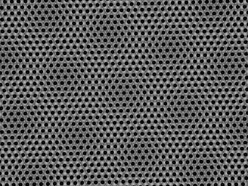


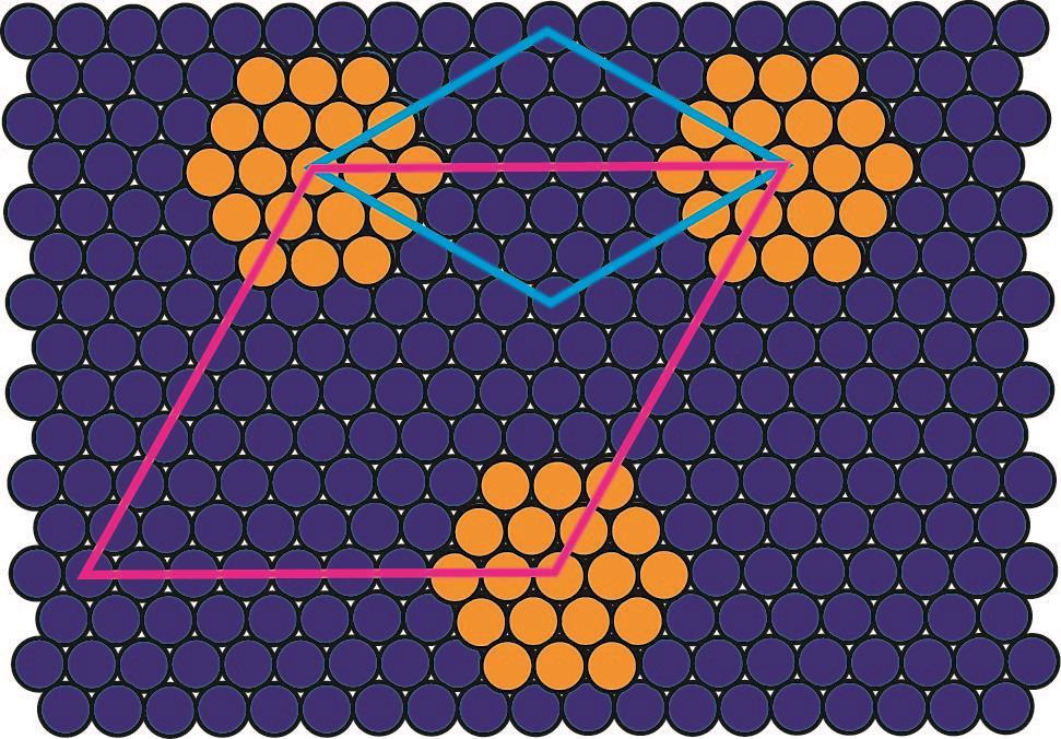
11 Scanning Probe Microscopy (STM) Moiré structures Moiré superstructures depend on: Lattice mismatch Overlayer rotation 6 7


12 FeO(111) 8x79Å HCP FCC TOP Fe-Fe: 3.09 Å Pt-Pt:.77 Å
 projected to the position of the tip apex above the surface.")
13 Limitations of the Tersoff-Haman approach Scanning Probe Microscopy (STM) In the simple, approximate model of Tersoff and Hamann, a direct correlation exists between the STM tunnel current and the energyintegrated local density of states (LDOS) projected to the position of the tip apex above the surface. Tersoff and Hamann: I V0 LDOSs EF, r 0 Tip state is not included in the Tersoff-Haman approach! STM topographs of FeO(111) measured with different tip states Merte, Besenbacher et al., Jour. Phys. Chem. C., 115, 089 (011)


14 Tip dependent imaging The contrast observed in the STM images can depend severely on the state of the tip. This is not included in Tersoff-Haman simulations! Fe-mode O-mode I tot V 0 s E E F t F e a m Merte, Knudsen et al., Surface Science, 603, L15 (009)
 K.")
15 The NiAl(110) surface Scanning Probe Microscopy (STM) K. Hansen, PhD thesis 001, University of Aarhus
 Science, 308, 1440")
16 Tip dependent imaging II Scanning Probe Microscopy (STM) Science, 308, 1440 (005)


17 Organic molecules on surfaces Weigelt, Linderoth, Besenbacher et al., Nature Materials, 5, 11 (006)


")


18 Following a chemical reaction on a surface with STM Scanning Probe Microscopy (STM) Problems with STM movies Drift due to temp. changes The tip might affect the reaction No chemical sensitivity


19 .7 Å HCP/FCC.46 Å Graphene on Ir(111) TOP 5 Å 50x50 Å


20 Clusters on graphene Cluster nucleation in HCP sites sp 3 sp 0.5 ML Pt on graphene/ir(111) as grown, 380x380Å Ideal model system for studying the adsorption properties with averaging methods.

")
")

21 In-situ unpinning of Pt-clusters on supported by graphene/ir(111) Scanning Probe Microscopy (STM) Gerber, Knudsen et al., ACS Nano, 7, 00 (013)

< 10-10 mbar P(CO)=5")

22 CO stability cluster size S av = 7 atoms +1.1 L CO S av = 19 atoms +16 L CO P(CO)< mbar P(CO)= mbar S av = 38 atoms +0 L CO Gerber, Knudsen et al., ACS Nano, 7, 00 (013)


23 CO intercalation: Structure of CO on Ir(111) in the mbar regime 19 (0.7 ML) 8 1mbar CO, RT, 40 min (33 33) structure 0.79 ML Grånäs et al., Jour. Phys. Chem. C, 117, (013)


 Grånäs et al., Jour. Phys.")
24 CO intercalation: STM P(CO) = 1 mbar, room temperature, 40 min A B B A A: Islands and stripes Not intercalated B: Islands Intercalated Small islands are not intercalated CO intercalated CO/Ir(111) Grånäs et al., Jour. Phys. Chem. C, 117, (013)
 step => Stripes at lower step edge Grånäs et al., Jour. Phys. Chem.")
25 CO intercalation: stripes Scanning Probe Microscopy (STM) P(CO) = 1 mbar, room temperature, 40 min TOP: 11 FCC/HCP: 7 Observations: HCP/FCC: 4 Stripes mainly located in FCC/HCP domains When graphene cross Ir(111) step => Stripes at lower step edge Grånäs et al., Jour. Phys. Chem. C, 117, (013)


26 CO intercalation: model for stripes Grånäs et al., Jour. Phys. Chem. C, 117, (013)


27 Etching of ML graphene Scanning Probe Microscopy (STM) 70 nm mbar O 585 K
 30 L 80 L 30 L 670 L Observations C-atoms are exclusively removed from the step edges During")
28 Etching of 0.5 ML graphene Scanning Probe Microscopy (STM) 30 L 80 L 30 L 670 L Observations C-atoms are exclusively removed from the step edges During etching graphene is always intercalated by O- atoms. Free Gr edges are etches faster than Gr-Ir edges Schröder et al., Carbon, 96, 30 (016)

29 Etching of 1 ML graphene Scanning Probe Microscopy (STM) 750 L at 700 K 750 L at 745 K What is the atomic scale structure of these nucleation sites?


30 Etching of 1 ML graphene Etching always start where two additional moiré rows starts The starting point of two additional moiré rows signals 5-7 defects => 5-7 defects are the starting point for graphene etching


31 Conclusions Theoretical expression of the tunnel current: Examples: I tot V 0 s EF t EF E I V0 LDOSs F, r 0 e a m
STM spectroscopy (STS)
") STM spectroscopy (STS) di dv 4 e ( E ev, r) ( E ) M S F T F Basic concepts of STS. With the feedback circuit open the variation of the tunneling current due to the application of a small oscillating voltage
STM spectroscopy (STS) di dv 4 e ( E ev, r) ( E ) M S F T F Basic concepts of STS. With the feedback circuit open the variation of the tunneling current due to the application of a small oscillating voltage
2) Atom manipulation. Xe / Ni(110) Model: Experiment:
 Atom manipulation. Xe / Ni(110) Model: Experiment:") 2) Atom manipulation D. Eigler & E. Schweizer, Nature 344, 524 (1990) Xe / Ni(110) Model: Experiment: G.Meyer, et al. Applied Physics A 68, 125 (1999) First the tip is approached close to the adsorbate
2) Atom manipulation D. Eigler & E. Schweizer, Nature 344, 524 (1990) Xe / Ni(110) Model: Experiment: G.Meyer, et al. Applied Physics A 68, 125 (1999) First the tip is approached close to the adsorbate
Microscopical and Microanalytical Methods (NANO3)
") Microscopical and Microanalytical Methods (NANO3) 06.11.15 10:15-12:00 Introduction - SPM methods 13.11.15 10:15-12:00 STM 20.11.15 10:15-12:00 STS Erik Zupanič erik.zupanic@ijs.si stm.ijs.si 27.11.15
Microscopical and Microanalytical Methods (NANO3) 06.11.15 10:15-12:00 Introduction - SPM methods 13.11.15 10:15-12:00 STM 20.11.15 10:15-12:00 STS Erik Zupanič erik.zupanic@ijs.si stm.ijs.si 27.11.15
Scanning Tunneling Microscopy/Spectroscopy
 Scanning Tunneling Microscopy/Spectroscopy 0 Scanning Tunneling Microscope 1 Scanning Tunneling Microscope 2 Scanning Tunneling Microscope 3 Typical STM talk or paper... The differential conductance di/dv
STM: Scanning Tunneling Microscope
 STM: Scanning Tunneling Microscope Basic idea STM working principle Schematic representation of the sample-tip tunnel barrier Assume tip and sample described by two infinite plate electrodes Φ t +Φ s =
Theoretical Modelling and the Scanning Tunnelling Microscope
 Theoretical Modelling and the Scanning Tunnelling Microscope Rubén Pérez Departamento de Física Teórica de la Materia Condensada Universidad Autónoma de Madrid Curso Introducción a la Nanotecnología Máster
Scanning Tunneling Microscopy (STM)
") Page 1 of 8 Scanning Tunneling Microscopy (STM) This is the fastest growing surface analytical technique, which is replacing LEED as the surface imaging tool (certainly in UHV, air and liquid). STM has
Page 1 of 8 Scanning Tunneling Microscopy (STM) This is the fastest growing surface analytical technique, which is replacing LEED as the surface imaging tool (certainly in UHV, air and liquid). STM has
Intercalation of atoms or molecules in
 Oxygen Intercalation under Graphene on Ir(111): Energetics, Kinetics, and the Role of Graphene Edges Elin Grånäs, Jan Knudsen, Ulrike A. Schröder, Timm Gerber, Carsten Busse, Mohammad A. Arman, Karina
3.1 Electron tunneling theory
 Scanning Tunneling Microscope (STM) was invented in the 80s by two physicists: G. Binnig and H. Rorher. They got the Nobel Prize a few years later. This invention paved the way for new possibilities in
Scanning Tunneling Microscopy. how does STM work? the quantum mechanical picture example of images how can we understand what we see?
 Scanning Tunneling Microscopy how does STM work? the quantum mechanical picture example of images how can we understand what we see? Observation of adatom diffusion with a field ion microscope Scanning
8 Summary and outlook
 91 8 Summary and outlook The main task of present work was to investigate the growth, the atomic and the electronic structures of Co oxide as well as Mn oxide films on Ag(001) by means of STM/STS at LT
Scanning Tunneling Microscopy
 Scanning Tunneling Microscopy References: 1. G. Binnig, H. Rohrer, C. Gerber, and Weibel, Phys. Rev. Lett. 49, 57 (1982); and ibid 50, 120 (1983). 2. J. Chen, Introduction to Scanning Tunneling Microscopy,
Supporting Information: From Permeation to Cluster Arrays: Graphene on. Ir(111) Exposed to Carbon Vapor
 Exposed to Carbon Vapor") Supporting Information: From Permeation to Cluster Arrays: Graphene on Ir(111) Exposed to Carbon Vapor Charlotte Herbig,, Timo Knispel, Sabina Simon,, Ulrike A. Schröder, Antonio J. Martínez-Galera, Mohammad
Supporting Information: From Permeation to Cluster Arrays: Graphene on Ir(111) Exposed to Carbon Vapor Charlotte Herbig,, Timo Knispel, Sabina Simon,, Ulrike A. Schröder, Antonio J. Martínez-Galera, Mohammad
Scanning Tunneling Microscopy
 Scanning Tunneling Microscopy A scanning tunneling microscope (STM) is an instrument for imaging surfaces at the atomic level. Its development in 1981 earned its inventors, Gerd Binnig and Heinrich Rohrer
Scanning Tunneling Microscopy
 Scanning Tunneling Microscopy References: 1. G. Binnig, H. Rohrer, C. Gerber, and Weibel, Phys. Rev. Lett. 49, 57 (1982); and ibid 50, 120 (1983). 2. J. Chen, Introduction to Scanning Tunneling Microscopy,
Self-Assembly of Two-Dimensional Organic Networks Containing Heavy Metals (Pb, Bi) and Preparation of Spin-Polarized Scanning Tunneling Microscope
 and Preparation of Spin-Polarized Scanning Tunneling Microscope") MPhil Thesis Defense Self-Assembly of Two-Dimensional Organic Networks Containing Heavy Metals (Pb, Bi) and Preparation of Spin-Polarized Scanning Tunneling Microscope Presented by CHEN Cheng 12 th Aug.
MPhil Thesis Defense Self-Assembly of Two-Dimensional Organic Networks Containing Heavy Metals (Pb, Bi) and Preparation of Spin-Polarized Scanning Tunneling Microscope Presented by CHEN Cheng 12 th Aug.
Supplementary Figure 1: Change of scanning tunneling microscopy (STM) tip state. a, STM tip transited from blurred (the top dark zone) to orbital
 tip state. a, STM tip transited from blurred (the top dark zone) to orbital") Supplementary Figure 1: Change of scanning tunneling microscopy (STM) tip state. a, STM tip transited from blurred (the top dark zone) to orbital resolvable (the bright zone). b, Zoomedin tip-state changing
Supplementary Figure 1: Change of scanning tunneling microscopy (STM) tip state. a, STM tip transited from blurred (the top dark zone) to orbital resolvable (the bright zone). b, Zoomedin tip-state changing
Spectroscopy at nanometer scale
 Spectroscopy at nanometer scale 1. Physics of the spectroscopies 2. Spectroscopies for the bulk materials 3. Experimental setups for the spectroscopies 4. Physics and Chemistry of nanomaterials Various
The basics of Scanning Probe Microscopy
 McGill University, Montreal, Jan. 8 th 2009 The basics of Scanning Probe Microscopy Federico Rosei Canada Research Chair in Nanostructured Organic and Inorganic Materials Énergie, Matériaux et Télécommunications,
Microscopy and Spectroscopy with Tunneling Electrons STM. Sfb Kolloquium 23rd October 2007
 Microscopy and Spectroscopy with Tunneling Electrons STM Sfb Kolloquium 23rd October 2007 The Tunnel effect T ( E) exp( S Φ E ) Barrier width s Barrier heigth Development: The Inventors 1981 Development:
Scanning Tunneling Microscopy. Wei-Bin Su, Institute of Physics, Academia Sinica
 Scanning Tunneling Microscopy Wei-Bin Su, Institute of Physics, Academia Sinica Tunneling effect Classical physics Field emission 1000 ~ 10000 V E V metal-vacuum-metal tunneling metal metal Quantum physics
tunneling theory of few interacting atoms in a trap
 tunneling theory of few interacting atoms in a trap Massimo Rontani CNR-NANO Research Center S3, Modena, Italy www.nano.cnr.it Pino D Amico, Andrea Secchi, Elisa Molinari G. Maruccio, M. Janson, C. Meyer,
Scanning probe microscopy of graphene with a CO terminated tip
 Scanning probe microscopy of graphene with a CO terminated tip Andrea Donarini T. Hofmann, A. J. Weymouth, F. Gießibl 7.5.2014 - Theory Group Seminar The sample Single monolayer of graphene Epitaxial growth
AFM: Atomic Force Microscopy II
 AM: Atomic orce Microscopy II Jan Knudsen The MAX IV laboratory & Division of synchrotron radiation research K522-523 (Sljus) 4 th of May, 2018 http://www.sljus.lu.se/staff/rainer/spm.htm Last time: The
Hydrogenated Graphene
 Hydrogenated Graphene Stefan Heun NEST, Istituto Nanoscienze-CNR and Scuola Normale Superiore Pisa, Italy Outline Epitaxial Graphene Hydrogen Chemisorbed on Graphene Hydrogen-Intercalated Graphene Outline
High resolution STM imaging with oriented single crystalline tips
 High resolution STM imaging with oriented single crystalline tips A. N. Chaika a, *, S. S. Nazin a, V. N. Semenov a, N. N Orlova a, S. I. Bozhko a,b, O. Lübben b, S. A. Krasnikov b, K. Radican b, and I.
Supplementary information
 Supplementary information Supplementary Figure S1STM images of four GNBs and their corresponding STS spectra. a-d, STM images of four GNBs are shown in the left side. The experimental STS data with respective
Solid Surfaces, Interfaces and Thin Films
 Hans Lüth Solid Surfaces, Interfaces and Thin Films Fifth Edition With 427 Figures.2e Springer Contents 1 Surface and Interface Physics: Its Definition and Importance... 1 Panel I: Ultrahigh Vacuum (UHV)
Graphene intercalation and chemical functionalization. Liv Hornekær
 Graphene intercalation and chemical functionalization Liv Hornekær Graphene Graphene - properties 1 Atom layer thin Very strong High thermal conductivity Optical absorption: pa Thermally and chemically
Surface Physics Surface Diffusion. Assistant: Dr. Enrico Gnecco NCCR Nanoscale Science
 Surface Physics 008 8. Surface Diffusion Assistant: Dr. Enrico Gnecco NCCR Nanoscale Science Random-Walk Motion Thermal motion of an adatom on an ideal crystal surface: - Thermal excitation the adatom
Scanning Probe Microscopy (SPM)
") http://ww2.sljus.lu.se/staff/rainer/spm.htm Scanning Probe Microscopy (FYST42 / FAFN30) Scanning Probe Microscopy (SPM) overview & general principles March 23 th, 2018 Jan Knudsen, room K522, jan.knudsen@sljus.lu.se
http://ww2.sljus.lu.se/staff/rainer/spm.htm Scanning Probe Microscopy (FYST42 / FAFN30) Scanning Probe Microscopy (SPM) overview & general principles March 23 th, 2018 Jan Knudsen, room K522, jan.knudsen@sljus.lu.se
Water clustering on nanostructured iron oxide films
 ARTICLE Received 12 May 2013 Accepted 22 May 2014 Published 30 Jun 2014 Water clustering on nanostructured iron oxide films Lindsay R. Merte1,2, Ralf Bechstein1, W. Guowen Peng3, Felix Rieboldt1, Carrie
Interpretation of STM
 Interpretation of STM František Máca X. NEVF 514 Surface Physics Winter Term 2011-2012 Troja, 16th December 2011 MOD NiFe TH Bard InAs Praha, December 16, 2011 p. 1 Scanning Tunnelling Microscopy Optimist
Surface Studies by Scanning Tunneling Microscopy
 Surface Studies by Scanning Tunneling Microscopy G. Binnig, H. Rohrer, Ch. Gerber, and E. Weibel IBM Zurich Research Laboratory, 8803 Ruschlikon-ZH, Switzerland (Received by Phys. Rev. Lett. on 30th April,
Symmetry Driven Band Gap Engineering in. Hydrogen Functionalized Graphene
 Symmetry Driven Band Gap Engineering in Hydrogen Functionalized Graphene Jakob H. Jørgensen 1, Antonija Grubišić Čabo 1, Richard Balog 1,2, Line Kyhl 1, Michael Groves 1, Andrew Cassidy 1, Albert Bruix
Electron transport simulations from first principles
 Electron transport simulations from first principles Krisztián Palotás Budapest University of Technology and Economics Department of Theoretical Physics Budapest, Hungary Methods Tunneling & ballistic
tip of a current tip and the sample. Components: 3. Coarse sample-to-tip isolation system, and
 SCANNING TUNNELING MICROSCOPE Brief history: Heinrich Rohrer and Gerd K. Binnig, scientists at IBM's Zurich Research Laboratory in Switzerland, are awarded the 1986 Nobel Prize in physicss for their work
Understanding water film assisted CO intercalation underneath Ir(111) supported graphene. Jonathan Peterson
 supported graphene. Jonathan Peterson") Understanding water film assisted CO intercalation underneath Ir(111) supported graphene Jonathan Peterson Thesis submitted for the degree of Bachelor of Science Project duration: 4 months Project supervised
Understanding water film assisted CO intercalation underneath Ir(111) supported graphene Jonathan Peterson Thesis submitted for the degree of Bachelor of Science Project duration: 4 months Project supervised
Local spectroscopy. N. Witkowski W. Sacks
 Local spectroscopy N. Witkowski W. Sacks Outlook 1. STM/STS theory elements a. history of STM and basic idea b. tunnel effect c. STM/STS 2. Technology a. STM design : vibration and thermal drift b. STM
Adsorption, desorption, and diffusion on surfaces. Joachim Schnadt Divsion of Synchrotron Radiation Research Department of Physics
 Adsorption, desorption, and diffusion on surfaces Joachim Schnadt Divsion of Synchrotron Radiation Research Department of Physics Adsorption and desorption Adsorption Desorption Chemisorption: formation
Application of single crystalline tungsten for fabrication of high resolution STM probes with controlled structure 1
 Application of single crystalline tungsten for fabrication of high resolution STM probes with controlled structure 1 A. N. Chaika a, S. S. Nazin a, V. N. Semenov a, V. G. Glebovskiy a, S. I. Bozhko a,b,
High Resolution Photoemission Study of the Spin-Dependent Band Structure of Permalloy and Ni
 High Resolution Photoemission Study of the Spin-Dependent Band Structure of Permalloy and Ni K. N. Altmann, D. Y. Petrovykh, and F. J. Himpsel Department of Physics, University of Wisconsin, Madison, 1150
Experimental methods in physics. Local probe microscopies I
 Experimental methods in physics Local probe microscopies I Scanning tunnelling microscopy (STM) Jean-Marc Bonard Academic year 09-10 1. Scanning Tunneling Microscopy 1.1. Introduction Image of surface
Surface atoms/molecules of a material act as an interface to its surrounding environment;
 1 Chapter 1 Thesis Overview Surface atoms/molecules of a material act as an interface to its surrounding environment; their properties are often complicated by external adsorbates/species on the surface
Electron confinement in metallic nanostructures
 Electron confinement in metallic nanostructures Pierre Mallet LEPES-CNRS associated with Joseph Fourier University Grenoble (France) Co-workers : Jean-Yves Veuillen, Stéphane Pons http://lepes.polycnrs-gre.fr/
Scanning Tunneling Microscopy Studies of the Ge(111) Surface
 Surface") VC Scanning Tunneling Microscopy Studies of the Ge(111) Surface Anna Rosen University of California, Berkeley Advisor: Dr. Shirley Chiang University of California, Davis August 24, 2007 Abstract: This
VC Scanning Tunneling Microscopy Studies of the Ge(111) Surface Anna Rosen University of California, Berkeley Advisor: Dr. Shirley Chiang University of California, Davis August 24, 2007 Abstract: This
Curriculum Vitae December 2006
 Appendix: (A brief description of some representative results) (1) Electronic states of Pb adatom and Pb adatom chains on Pb(111) have been investigated by spatially scanning tunneling spectroscopy (STS)
SUPPLEMENTARY INFORMATION
 DOI: 10.1038/NCHEM.2491 Experimental Realization of Two-dimensional Boron Sheets Baojie Feng 1, Jin Zhang 1, Qing Zhong 1, Wenbin Li 1, Shuai Li 1, Hui Li 1, Peng Cheng 1, Sheng Meng 1,2, Lan Chen 1 and
Visualization of atomic-scale phenomena in superconductors
 Visualization of atomic-scale phenomena in superconductors Andreas Kreisel, Brian Andersen Niels Bohr Institute, University of Copenhagen, 2100 København, Denmark Peayush Choubey, Peter Hirschfeld Department
(Scanning Probe Microscopy)
") (Scanning Probe Microscopy) Ing-Shouh Hwang (ishwang@phys.sinica.edu.tw) Institute of Physics, Academia Sinica, Taipei, Taiwan References 1. G. Binnig, H. Rohrer, C. Gerber, and Weibel, Phys. Rev. Lett.
(Scanning Probe Microscopy) Ing-Shouh Hwang (ishwang@phys.sinica.edu.tw) Institute of Physics, Academia Sinica, Taipei, Taiwan References 1. G. Binnig, H. Rohrer, C. Gerber, and Weibel, Phys. Rev. Lett.
Scanning tunneling microscopy
 IFM The Department of Physics, Chemistry and Biology Lab 72 in TFFM08 Scanning tunneling microscopy NAME PERS. - NUMBER DATE APPROVED Rev. Dec 2006 Ivy Razado Aug 2014 Tuomas Hänninen Contents 1 Introduction
Self-assembly of molecules on surfaces. Manuel Alcamí Departamento de Química Universidad Autónoma de Madrid
 Self-assembly of molecules on surfaces Manuel Alcamí Departamento de Química Universidad Autónoma de Madrid Outline Outline Motivation Examples of molecules deposited on surfaces Graphene/Ru(0001) TQ /
Program Operacyjny Kapitał Ludzki SCANNING PROBE TECHNIQUES - INTRODUCTION
 Program Operacyjny Kapitał Ludzki SCANNING PROBE TECHNIQUES - INTRODUCTION Peter Liljeroth Department of Applied Physics, Aalto University School of Science peter.liljeroth@aalto.fi Projekt współfinansowany
Special Properties of Au Nanoparticles
 Special Properties of Au Nanoparticles Maryam Ebrahimi Chem 7500/750 March 28 th, 2007 1 Outline Introduction The importance of unexpected electronic, geometric, and chemical properties of nanoparticles
Introduction to Scanning Tunneling Microscopy
 Introduction to Scanning Tunneling Microscopy C. JULIAN CHEN IBM Research Division Thomas J. Watson Research Center Yorktown Heights, New York New York Oxford OXFORD UNIVERSITY PRESS 1993 CONTENTS List
SUPPLEMENTARY INFORMATION
 SUPPLEMENTARY INFORMATION Method: Epitaxial graphene was prepared by heating an Ir(111) crystal to 550 K for 100 s under 2 x 10⁻⁵ Pa partial pressure of ethylene, followed by a flash anneal to 1420 K 1.
MPI Stuttgart. Atomic-scale control of graphene magnetism using hydrogen atoms. HiMagGraphene.
 MPI Stuttgart Atomic-scale control of graphene magnetism using hydrogen atoms HiMagGraphene ivan.brihuega@uam.es www.ivanbrihuega.com Budapest, April, 2016 Magnetism in graphene: just remove a p z orbital
STM and graphene. W. W. Larry Pai ( 白偉武 ) Center for condensed matter sciences, National Taiwan University NTHU, 2013/05/23
 Center for condensed matter sciences, National Taiwan University NTHU, 2013/05/23") STM and graphene W. W. Larry Pai ( 白偉武 ) Center for condensed matter sciences, National Taiwan University NTHU, 2013/05/23 Why graphene is important: It is a new form of material (two dimensional, single
STM and graphene W. W. Larry Pai ( 白偉武 ) Center for condensed matter sciences, National Taiwan University NTHU, 2013/05/23 Why graphene is important: It is a new form of material (two dimensional, single
Imaging Methods: Scanning Force Microscopy (SFM / AFM)
") Imaging Methods: Scanning Force Microscopy (SFM / AFM) The atomic force microscope (AFM) probes the surface of a sample with a sharp tip, a couple of microns long and often less than 100 Å in diameter.
Imaging Methods: Scanning Force Microscopy (SFM / AFM) The atomic force microscope (AFM) probes the surface of a sample with a sharp tip, a couple of microns long and often less than 100 Å in diameter.
Chapter 103 Spin-Polarized Scanning Tunneling Microscopy
 Chapter 103 Spin-Polarized Scanning Tunneling Microscopy Toyo Kazu Yamada Keywords Spin-polarized tunneling current Spin polarization Magnetism 103.1 Principle Spin-polarized scanning tunneling microscopy
Scanning Tunneling Microscopy
 Scanning Tunneling Microscopy References: 1. G. Binnig, H. Rohrer, C. Gerber, and Weibel, Phys. Rev. Lett. 49, 57 (1982); and ibid 50, 120 (1983). 2. J. Chen, Introduction to Scanning Tunneling Microscopy,
Supplementary Figure 1 Experimental setup for crystal growth. Schematic drawing of the experimental setup for C 8 -BTBT crystal growth.
 Supplementary Figure 1 Experimental setup for crystal growth. Schematic drawing of the experimental setup for C 8 -BTBT crystal growth. Supplementary Figure 2 AFM study of the C 8 -BTBT crystal growth
Spectroscopy of Nanostructures. Angle-resolved Photoemission (ARPES, UPS)
") Spectroscopy of Nanostructures Angle-resolved Photoemission (ARPES, UPS) Measures all quantum numbers of an electron in a solid. E, k x,y, z, point group, spin E kin, ϑ,ϕ, hν, polarization, spin Electron
Spectroscopy of Nanostructures Angle-resolved Photoemission (ARPES, UPS) Measures all quantum numbers of an electron in a solid. E, k x,y, z, point group, spin E kin, ϑ,ϕ, hν, polarization, spin Electron
Lecture 3: Electron statistics in a solid
 Lecture 3: Electron statistics in a solid Contents Density of states. DOS in a 3D uniform solid.................... 3.2 DOS for a 2D solid........................ 4.3 DOS for a D solid........................
Initial Stages of Growth of Organic Semiconductors on Graphene
 Initial Stages of Growth of Organic Semiconductors on Graphene Presented by: Manisha Chhikara Supervisor: Prof. Dr. Gvido Bratina University of Nova Gorica Outline Introduction to Graphene Fabrication
Supplementary Information for Solution-Synthesized Chevron Graphene Nanoribbons Exfoliated onto H:Si(100)
") Supplementary Information for Solution-Synthesized Chevron Graphene Nanoribbons Exfoliated onto H:Si(100) Adrian Radocea,, Tao Sun,, Timothy H. Vo, Alexander Sinitskii,,# Narayana R. Aluru,, and Joseph
Supplementary Information for Solution-Synthesized Chevron Graphene Nanoribbons Exfoliated onto H:Si(100) Adrian Radocea,, Tao Sun,, Timothy H. Vo, Alexander Sinitskii,,# Narayana R. Aluru,, and Joseph
SUPPLEMENTARY INFORMATION
 In the format provided by the authors and unedited. Intrinsically patterned two-dimensional materials for selective adsorption of molecules and nanoclusters X. Lin 1,, J. C. Lu 1,, Y. Shao 1,, Y. Y. Zhang
A Scanning Tunneling Microscopy Study on Atomic Carbon and Nitrogen on Pt(111) By Zhu Liang B.S., Peking University, 2009 THESIS
 By Zhu Liang B.S., Peking University, 2009 THESIS") A Scanning Tunneling Microscopy Study on Atomic Carbon and Nitrogen on Pt(111) By Zhu Liang B.S., Peking University, 2009 THESIS Submitted as partial fulfillment of the requirements for the degree of Doctor
A Scanning Tunneling Microscopy Study on Atomic Carbon and Nitrogen on Pt(111) By Zhu Liang B.S., Peking University, 2009 THESIS Submitted as partial fulfillment of the requirements for the degree of Doctor
Instrumentation and Operation
 Instrumentation and Operation 1 STM Instrumentation COMPONENTS sharp metal tip scanning system and control electronics feedback electronics (keeps tunneling current constant) image processing system data
Scanning Probe Microscopies (SPM)
") Scanning Probe Microscopies (SPM) Nanoscale resolution af objects at solid surfaces can be reached with scanning probe microscopes. They allow to record an image of the surface atomic arrangement in direct
Scanning Probe Microscopies (SPM) Nanoscale resolution af objects at solid surfaces can be reached with scanning probe microscopes. They allow to record an image of the surface atomic arrangement in direct
INTRODUCTION TO SCA\ \I\G TUNNELING MICROSCOPY
 INTRODUCTION TO SCA\ \I\G TUNNELING MICROSCOPY SECOND EDITION C. JULIAN CHEN Department of Applied Physics and Applied Mathematics, Columbia University, New York OXFORD UNIVERSITY PRESS Contents Preface
Scanning tunneling microscopy of monoatomic gold chains on vicinal Si(335) surface: experimental and theoretical study
 surface: experimental and theoretical study") phys. stat. sol. (b) 4, No., 33 336 (005) / DOI 10.100/pssb.00460056 Scanning tunneling microscopy of monoatomic gold chains on vicinal Si(335) surface: experimental and theoretical study M. Krawiec *,
phys. stat. sol. (b) 4, No., 33 336 (005) / DOI 10.100/pssb.00460056 Scanning tunneling microscopy of monoatomic gold chains on vicinal Si(335) surface: experimental and theoretical study M. Krawiec *,
Honeycomb lattice of graphite probed by scanning tunneling microscopy with a carbon
 1 Honeycomb lattice of graphite probed by scanning tunneling microscopy with a carbon nanotube tip Jeehoon Kim, Junwei Huang, and Alex de Lozanne* Department of Physics, The University of Texas, TX 78712
Tuning magnetic anisotropy, Kondo screening and Dzyaloshinskii-Moriya interaction in pairs of Fe adatoms
 Tuning magnetic anisotropy, Kondo screening and Dzyaloshinskii-Moriya interaction in pairs of Fe adatoms Department of Physics, Hamburg University, Hamburg, Germany SPICE Workshop, Mainz Outline Tune magnetic
Scanning Probe Microscopy
 1 Scanning Probe Microscopy Dr. Benjamin Dwir Laboratory of Physics of Nanostructures (LPN) Benjamin.dwir@epfl.ch PH.D3.344 Outline: Introduction: What is SPM, history STM AFM Image treatment Advanced
Supplementary information for Probing atomic structure and Majorana wavefunctions in mono-atomic Fe chains on superconducting Pb surface
 Supplementary information for Probing atomic structure and Majorana wavefunctions in mono-atomic Fe chains on superconducting Pb surface Rémy Pawlak 1, Marcin Kisiel 1, Jelena Klinovaja 1, Tobias Meier
Chapter 2. Theoretical background. 2.1 Itinerant ferromagnets and antiferromagnets
 Chapter 2 Theoretical background The first part of this chapter gives an overview of the main static magnetic behavior of itinerant ferromagnetic and antiferromagnetic materials. The formation of the magnetic
A structural study of the phases occurring on the Ag(111)-Sb system
-Sb system") A structural study of the phases occurring on the Ag(111)-Sb system V. B. Nascimento, 1 E. A. Soares 1, C. Bitencourt 3, V. E. de Carvalho 1, C. M. C. de Castilho 2, C. F. MacConville 3, D. P. Woodruff
A structural study of the phases occurring on the Ag(111)-Sb system V. B. Nascimento, 1 E. A. Soares 1, C. Bitencourt 3, V. E. de Carvalho 1, C. M. C. de Castilho 2, C. F. MacConville 3, D. P. Woodruff
Pb thin films on Si(111): Local density of states and defects
: Local density of states and defects") University of Wollongong Research Online Australian Institute for Innovative Materials - Papers Australian Institute for Innovative Materials 2014 Pb thin films on Si(111): Local density of states and
University of Wollongong Research Online Australian Institute for Innovative Materials - Papers Australian Institute for Innovative Materials 2014 Pb thin films on Si(111): Local density of states and
Hydrogen Storage in Metalfunctionalized
 Hydrogen Storage in Metalfunctionalized Graphene Stefan Heun NEST, Istituto Nanoscienze-CNR and Scuola Normale Superiore Pisa, Italy Outline Introduction to Hydrogen Storage Epitaxial Graphene Hydrogen
The interpretation of STM images in light of Tersoff and Hamann tunneling model
 The interpretation of STM images in light of Tersoff and Hamann tunneling model The STM image represents contour maps of constant surface LDOS at E F, evaluated at the center of the curvature of the tip.
An account of our efforts towards air quality monitoring in epitaxial graphene on SiC
 European Network on New Sensing Technologies for Air Pollution Control and Environmental Sustainability - EuNetAir COST Action TD1105 2 nd International Workshop EuNetAir on New Sensing Technologies for
Energy Spectroscopy. Ex.: Fe/MgO
 Energy Spectroscopy Spectroscopy gives access to the electronic properties (and thus chemistry, magnetism,..) of the investigated system with thickness dependence Ex.: Fe/MgO Fe O Mg Control of the oxidation
Implementation of spin detection in a commercial low temperature scanning tunneling microscope
 Eindhoven University of Technology MASTER Implementation of spin detection in a commercial low temperature scanning tunneling microscope Keizer, J.G. Award date: 2007 Disclaimer This document contains
Identifying and Visualizing the Edge Terminations of Single-Layer MoSe2 Island Epitaxially Grown on Au(111)
") Supporting Information Identifying and Visualizing the Edge Terminations of Single-Layer MoSe2 Island Epitaxially Grown on Au(111) Jianchen Lu, De-Liang Bao, Kai Qian, Shuai Zhang, Hui Chen, Xiao Lin*,
Supporting Information Identifying and Visualizing the Edge Terminations of Single-Layer MoSe2 Island Epitaxially Grown on Au(111) Jianchen Lu, De-Liang Bao, Kai Qian, Shuai Zhang, Hui Chen, Xiao Lin*,
Lattice-matched versus lattice-mismatched models to describe epitaxial monolayer graphene on Ru(0001) REVIEW COPY
 REVIEW COPY") Lattice-matched versus lattice-mismatched models to describe epitaxial monolayer graphene on Ru(0001) D. Stradi, 1,2 S. Barja, 3,2 C. Díaz, 1 M. Garnica, 3,2 B. Borca, 3 J. J. Hinarejos, 3 D. Sánchez-Portal,
Lattice-matched versus lattice-mismatched models to describe epitaxial monolayer graphene on Ru(0001) D. Stradi, 1,2 S. Barja, 3,2 C. Díaz, 1 M. Garnica, 3,2 B. Borca, 3 J. J. Hinarejos, 3 D. Sánchez-Portal,
Lecture 26 MNS 102: Techniques for Materials and Nano Sciences
 Lecture 26 MNS 102: Techniques for Materials and Nano Sciences Reference: #1 C. R. Brundle, C. A. Evans, S. Wilson, "Encyclopedia of Materials Characterization", Butterworth-Heinemann, Toronto (1992),
Supplementary Materials for
 advances.sciencemag.org/cgi/content/full/3/10/e1701661/dc1 Supplementary Materials for Defect passivation of transition metal dichalcogenides via a charge transfer van der Waals interface Jun Hong Park,
Molecular Beam Epitaxy Growth of Tetragonal FeS Film on
 Molecular Beam Epitaxy Growth of Tetragonal FeS Film on SrTiO3(001) Substrate Kun Zhao( 赵琨 ) 1, Haicheng Lin( 林海城 ) 1, Wantong Huang( 黄万通 ) 1, Xiaopeng Hu( 胡小鹏 ) 1,2, Xi Chen( 陈曦 ) 1,2, Qi-Kun Xue( 薛其坤
Scanning Tunneling Microscopy
 Scanning Tunneling Microscopy Scanning Direction References: Classical Tunneling Quantum Mechanics Tunneling current Tunneling current I t I t (V/d)exp(-Aφ 1/2 d) A = 1.025 (ev) -1/2 Å -1 I t = 10 pa~10na
Scanning Probe Microscopy. EMSE-515 F. Ernst
 Scanning Probe Microscopy EMSE-515 F. Ernst 1 Literature 2 3 Scanning Probe Microscopy: The Lab on a Tip by Ernst Meyer,Ans Josef Hug,Roland Bennewitz 4 Scanning Probe Microscopy and Spectroscopy : Theory,
Supplementary Materials for Oxygen-induced self-assembly of quaterphenyl molecule on metal surfaces
 Electronic Supplementary Material (ESI) for ChemComm. This journal is The Royal Society of Chemistry 2014 Supplementary Materials for Oxygen-induced self-assembly of quaterphenyl molecule on metal surfaces
Designing Graphene for Hydrogen Storage
 Designing Graphene for Hydrogen Storage Stefan Heun NEST, Istituto Nanoscienze-CNR and Scuola Normale Superiore Pisa, Italy Outline Introduction to Hydrogen Storage Epitaxial Graphene Hydrogen Storage
Supplementary Figure 1
 Supplementary Figure 1 0.4 0.2 a 0.0 Averaged di/dv-asymmetry -0.2-0.4 0.04 0.02 0.00-0.02-0.04-0.06-0.2 b Co core 0.0 0.2 0.4 di/dv asymmetry Spin polarization 0.4 0.2 0.0-0.2-0.4-0.6 Spin polarization
Electronic states on the surface of graphite
 Electronic states on the surface of graphite Guohong Li, Adina Luican, Eva Y. Andrei * Department of Physics and Astronomy, Rutgers Univsersity, Piscataway, NJ 08854, USA Elsevier use only: Received date
Graphene and Boron Nitride Single Layers
 arxiv:0904.1520v1 [cond-mat.mtrl-sci] 9 Apr 2009 Graphene and Boron Nitride Single Layers April 9, 2009 Thomas Greber, Physik Institut, Universität Zürich, Switzerland Uni Irchel 36K88, +41 44 635 5744,
Southeast University, Nanjing, China 2 Department of Applied Physics, Aalto University,
 Supplementary Information to Solubility of Boron, Carbon and Nitrogen in Transition Metals: Getting Insight into Trends from First-Principles Calculations Xiaohui Hu, 1,2 Torbjörn Björkman 2,3, Harri Lipsanen
SUPPLEMENTARY INFORMATION
 SUPPLEMENTARY INFORMATION Transforming Fullerene into Graphene Quantum Dots Jiong Lu, Pei Shan Emmeline Yeo, Chee Kwan Gan, Ping Wu and Kian Ping Loh email: chmlohkp@nus.edu.sg Contents Figure S1 Transformation
SUPPLEMENTARY INFORMATION
 In the format provided by the authors and unedited. DOI: 10.1038/NPHYS4186 Stripes Developed at the Strong Limit of Nematicity in FeSe film Wei Li 1,2,3*, Yan Zhang 2,3,4,5, Peng Deng 1, Zhilin Xu 1, S.-K.
Supporting Information for Ultra-narrow metallic armchair graphene nanoribbons
 Supporting Information for Ultra-narrow metallic armchair graphene nanoribbons Supplementary Figure 1 Ribbon length statistics. Distribution of the ribbon lengths and the fraction of kinked ribbons for