Designing Graphene for Hydrogen Storage
|
|
|
- Gabriella Warner
- 5 years ago
- Views:
Transcription

1 Designing Graphene for Hydrogen Storage Stefan Heun NEST, Istituto Nanoscienze-CNR and Scuola Normale Superiore Pisa, Italy
2 Outline Introduction to Hydrogen Storage Epitaxial Graphene Hydrogen Storage by Corrugation Hydrogen Storage by Functionalization
3 Outline Introduction to Hydrogen Storage Epitaxial Graphene Hydrogen Storage by Corrugation Hydrogen Storage by Functionalization

4 Hydrogen Life Cycle Complete energy loop relying on renewable sources Hydrogen Storage in a safe and cheap way is a critical issue
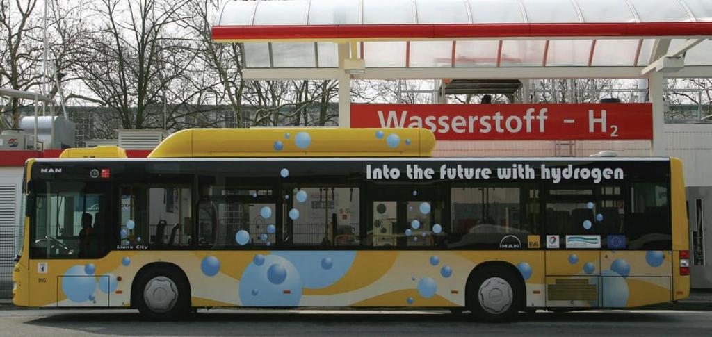

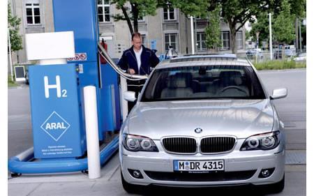
5 Hydrogen-fuelled vehicles
 Renewable, unlimited resource Reduction in CO 2 emission Reduction of oil dependency However, hydrogen is NOT an energy source: it must be produced e.g. by electrolysis, needing +2.")
6 Hydrogen & energy As a fuel, hydrogen has advantages: Highest energy-to-mass ratio H2 + 1/2 O2 H2O ΔH = -2.96eV Non-toxic and clean (product = water) Renewable, unlimited resource Reduction in CO 2 emission Reduction of oil dependency However, hydrogen is NOT an energy source: it must be produced e.g. by electrolysis, needing ev, with zero balance with respect to energy production. Hydrogen fuel cell

7 Hydrogen Storage Targets for transport applications not reached yet: r m > 5.5 wt% r V > 50 kg H 2 /m 3 P eq 1bar at T< 100 C Compressed H 2 : High pressure and heavy container to support such pressure Solid State: Physisorption Chemisorption Liquid H 2 : Liquefation needs energy and consumes more than 20% of the recoverable energy
 Functionalized graphene has been predicted to adsorb up to 9 wt% of hydrogen Yang et al.")
8 Graphene for hydrogen storage Graphene is lightweight, inexpensive, robust, chemically stable Large surface area (~ 2600 m 2 /g) Functionalized graphene has been predicted to adsorb up to 9 wt% of hydrogen Yang et al., PRB 79 (2009)
9 H storage in graphene Atomic hydrogen chemisorption has a small or negligible chemisorption barrier feasible but H2 must be cracked Physisorption weakly bounds hydrogen acceptable storage densities only at low temperatures and/or high pressure Molecular hydrogen chemi(de)sorption has high barrier (theoretical estimate ~ev) chemisorbed H is stable for transportation etc, but catalytic mechanisms are necessary in the loading-release phases V. Tozzini and V. Pellegrini: Phys. Chem. Chem. Phys. 15 (2013) 80.
10 Outline Introduction to Hydrogen Storage Epitaxial Graphene Hydrogen Storage by Corrugation Hydrogen Storage by Functionalization


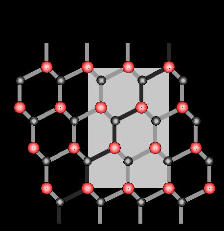
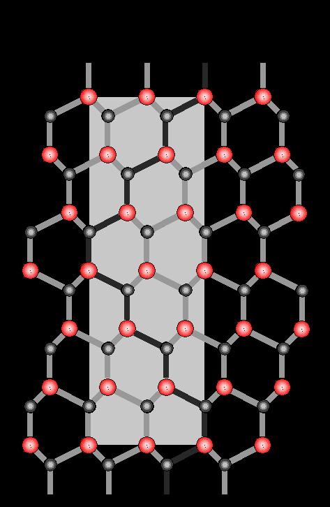
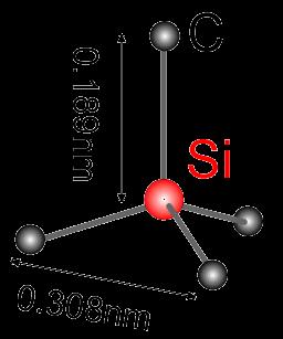
11 Silicon Carbide in a Nutshell Bilayer of Si-C tetrahedra SiC Polytypes Si-face SiC(0001) C-face SiC(0001)
12 Silicon Carbide in a Nutshell Bilayer of Si-C tetrahedra Si-face SiC(0001) Graphene: Ordered stacking Good thickness control C-face SiC(0001) Graphene: Rotational disorder Poor thickness control

.")

13 Graphene growth on SiC(0001) ML Buffer Layer Buffer Layer SiC SiC Buffer Layer Topologically identical atomic carbon structure as graphene. Does not have the electronic band structure of graphene due to periodic sp 3 C-Si bonds. F. Varchon, et al., PRB 77, (2008). Theoretical Calculations 6 3 x 6 3 F. Varchon, et al., PRB 77, (2008). Superstructure of both the buffer layer and monolayer graphene on the Si face from the periodic interaction with the substrate.


14 Buffer Layer Bias: +1.7V Current: 0.3nA quasi-(6x6) F. Varchon, et al., PRB 77, (2008) Å 2.0Å 2.00 S. Goler et al.: Carbon 51, 249 (2013).


15 Monolayer Graphene STM S. Goler et al.: J. Phys. Chem. C 117, (2013).

16 6 3x6 3-Superstructure Graphene SiC 30 nm, 1V, 100 pa E= 75 ev

17 Hydrogen Intercalation Buffer Layer ML SiC SiC Buffer Layer (BL) Quasi-free standing monolayer graphene Quartz tube P ~ atmospheric pressure T ~ 800 C H 2 C. Riedl, C. Coletti et al., PRL 103, (2009)
 S. Forti, et al., PRB 84, 125449 (2011). k (Å -1 ) p=2.")
18 Energy (ev) Energy (ev) Hydrogen Intercalation Buffer Layer ML SiC SiC E F = Buffer Layer (BL) Quasi-free standing monolayer graphene E F = k (Å -1 ) S. Forti, et al., PRB 84, (2011). k (Å -1 ) p= cm -2
.")
19 S. Goler et al.: Carbon 51, 249 (2013). BL vs. QFMLG
.")
20 S. Goler et al.: Carbon 51, 249 (2013). BL vs. QFMLG
21 Outline Introduction to Hydrogen Storage Epitaxial Graphene Hydrogen Storage by Corrugation Hydrogen Storage by Functionalization

22 Graphene Curvature Exploit graphene curvature for hydrogen storage at room temperature and pressure The hydrogen binding energy on graphene is strongly dependent on local curvature and it is larger on convex parts Atomic hydrogen spontaneously sticks on convex parts; inverting curvature H is expelled Hydrogen clusters on corrugated graphene V. Tozzini and V. Pellegrini: J. Phys. Chem. C 115, (2011).
23 Graphene Curvature Exploit graphene curvature for hydrogen storage at room temperature and pressure The hydrogen binding energy on graphene is strongly dependent on local curvature and it is larger on convex parts Atomic hydrogen spontaneously sticks on convex parts; inverting curvature H is expelled Hydrogen clusters on corrugated graphene V. Tozzini and V. Pellegrini: J. Phys. Chem. C 115, (2011).

24 Graphene Curvature Exploit graphene curvature for hydrogen storage at room temperature and pressure The hydrogen binding energy on graphene is strongly dependent on local curvature and it is larger on convex parts Atomic hydrogen spontaneously sticks on convex parts; inverting curvature H is expelled Hydrogen clusters on corrugated graphene V. Tozzini and V. Pellegrini: J. Phys. Chem. C 115, (2011).

25 H-dimers and tetramers Para-dimer Ortho-dimer Tetramer S. Goler et al.: J. Phys. Chem. C 117, (2013).
26 STS after hydrogenation S. Goler et al.: J. Phys. Chem. C 117, (2013).

27 H adsorption and desorption S. Goler et al.: J. Phys. Chem. C 117, (2013).
28 RMS roughness S. Goler et al.: J. Phys. Chem. C 117, (2013).
29 DFT calculations S. Goler et al.: J. Phys. Chem. C 117, (2013).
30 Outline Introduction to Hydrogen Storage Epitaxial Graphene Hydrogen Storage by Corrugation Hydrogen Storage by Functionalization

 793 Durgen et al.")
31 Functionalized Graphene Functionalized graphene has been predicted to adsorb up to 9 wt% of hydrogen Modify graphene with various chemical species, such as calcium or transition metals (Titanium) Lee et al., Nano Lett. 10 (2010) 793 Durgen et al., PRB 77 (2007)
 with reconstruction After")

32 Titanium on graphene ML graphene on SiC(0001) with reconstruction After deposition of Ti at RT T. Mashoff et al.: Appl. Phys. Lett. 103, (2013)


 6%")

33 A = e+02 +/ e+01 xc = e+00 +/ e-01 w = e+00 +/ e-01 y0 = e+00 +/ e+00 Titanium island growth Island diameter (nm) 6% Coverage 16% Coverage 29% Coverage 53% Coverage 79% Coverage T. Mashoff et al.: Appl. Phys. Lett. 103, (2013) 100% Coverage
34 Thermal desorption spectroscopy Deposition of different amounts of Titanium Offering Hydrogen (D 2 ) (1x10⁻⁷ mbar for 5 min) Heating sample with constant rate (10K/s) up to 550 C Measuring masssensitive desorption with a mass spectrometer Spectra for different Ti-coverages Desorption signal (a. u.) 0 100% 79% 53% 29% 16% 6% Temperature (C) T. Mashoff et al.: Appl. Phys. Lett. 103, (2013)


35 nm Forming of Islands 1 nm 100 nm, 1 V, 82 pa nm
36 DCV = Double Carbon Vacancy


37 N 2 - sputtering of the graphene surface Clean graphene surface Sputtered 10x10 nm 2, 1V, 0.8nA 10x10 nm 2, 1V, 0.8nA Defects in the graphene film should reduce the mobility of Tiatoms and lead to more and smaller islands.
 1 0 100 200 300 400 500 Sputter time (s) Energy: 200eV, Ion Current: (5.7 +/- 1) na")
38 Number of Defects Size (nm 2 ) Distribution of defects in graphene Number of Defects per 100nm 2 Average size of defects Sputter time (s) Sputter time (s) Energy: 200eV, Ion Current: (5.7 +/- 1) na
39 Number of defects Average number of induced defects per 100nm Sputter energy (ev) Sputter time: 150s

 Sputtered 150 s and Deposition")
40 Number of islands Average Number of Islands per 100 nm Sputter Energy (ev) Sputtered 150 s and Deposition of 0.5 ML Titanium
41 Island diameter (nm) Average diameter of individual Ti-Islands Sputter Energy (ev)
42 Total Island Surface (nm 2 ) Active 3D-surface per 100nm Sputter energy (ev)
43 Conclusions Graphene is a promising material for hydrogen storage Curvature-dependent adsorption and desorption of hydrogen reusable hydrogen storage devices that do not depend on temperature or pressure changes. Graphene functionalized by Ti: Stability of hydrogen binding at room temperature Hydrogen desorbes at moderate temperatures Modifying the size and distribution of Islands by sputtering and increasing the active surface


44 Acknowledgements S. Goler T. Mashoff D. Convertino V. Miseikis C. Coletti V. Piazza V. Tozzini P. Pingue F. Colangelo V. Pellegrini F. Beltram K. V. Emtsev, U. Starke, S. Forti M. Takamura S. Tanabe H. Hibino


45 Acknowledgements Sarah Goler, Torge Mashoff, Domenica Convertino, Vaidotas Miseikis, Camilla Coletti, Vincenzo Piazza, Valentina Tozzini, Francesco Colangelo, Pasquale Pingue, Vittorio Pellegrini, Fabio Beltram Makoto Takamura, Shinichi Tanabe, Hiroki Hibino Konstantin V. Emtsev, Stiven Forti, Ulrich Starke Funding:
Hydrogen Storage in Metalfunctionalized
 Hydrogen Storage in Metalfunctionalized Graphene Stefan Heun NEST, Istituto Nanoscienze-CNR and Scuola Normale Superiore Pisa, Italy Outline Introduction to Hydrogen Storage Epitaxial Graphene Hydrogen
Hydrogenated Graphene
 Hydrogenated Graphene Stefan Heun NEST, Istituto Nanoscienze-CNR and Scuola Normale Superiore Pisa, Italy Outline Epitaxial Graphene Hydrogen Chemisorbed on Graphene Hydrogen-Intercalated Graphene Outline
Metal-functionalized Graphene for Hydrogen Storage
 Metal-functionalized Graphene for Hydrogen Storage Stefan Heun NEST, Istituto Nanoscienze-CNR and Scuola Normale Superiore Pisa, Italy NEST Pisa Research themes @ NEST Pisa National Enterprise for nanoscience
Laurea degree (summa cum laude) in physics from the University of Pisa, in 1992 and the PhD in physics from Scuola Normale Superiore of Pisa, in 1997
 in physics from the University of Pisa, in 1992 and the PhD in physics from Scuola Normale Superiore of Pisa, in 1997") Vittorio PELLEGRINI Graphene for energy applications Laurea degree (summa cum laude) in physics from the University of Pisa, in 1992 and the PhD in physics from Scuola Normale Superiore of Pisa, in 1997
Vittorio PELLEGRINI Graphene for energy applications Laurea degree (summa cum laude) in physics from the University of Pisa, in 1992 and the PhD in physics from Scuola Normale Superiore of Pisa, in 1997
Revealing the nature of defects in quasi free standing monolayer graphene on SiC(0001) by means of Density Functional Theory
 by means of Density Functional Theory") Revealing the nature of defects in quasi free standing monolayer graphene on SiC(0001) by means of Density Functional Theory Tommaso Cavallucci, 1 Yuya Murata, 1 Makoto Takamura, 2 Hiroki Hibino, 2, Stefan
Revealing the nature of defects in quasi free standing monolayer graphene on SiC(0001) by means of Density Functional Theory Tommaso Cavallucci, 1 Yuya Murata, 1 Makoto Takamura, 2 Hiroki Hibino, 2, Stefan
2D Materials Research Activities at the NEST lab in Pisa, Italy. Stefan Heun NEST, Istituto Nanoscienze-CNR and Scuola Normale Superiore, Pisa, Italy
 2D Materials Research Activities at the NEST lab in Pisa, Italy Stefan Heun NEST, Istituto Nanoscienze-CNR and Scuola Normale Superiore, Pisa, Italy 2D Materials Research Activities at the NEST lab in
MBE growth of self-assisted InAs nanowires on graphene
 MBE growth of self-assisted InAs nanowires on graphene Lucia Sorba NEST, Istituto Nanoscienze-CNR and Scuola Normale Superiore, Pisa. Italy 2 mm InAs NWs on Graphene InAs NWs are key role payers in the
Atomic and Electronic Structure of Si Dangling Bonds in Quasi-free Standing Monolayer Graphene
 Atomic and Electronic Structure of Si Dangling Bonds in Quasi-free Standing Monolayer Graphene Yuya Murata, 1 Tommaso Cavallucci, 1 Valentina Tozzini, 1 Niko Pavliček, 2 Leo Gross, 2 Gerhard Meyer, 2 Makoto
Outline. Introduction: graphene. Adsorption on graphene: - Chemisorption - Physisorption. Summary
 Outline Introduction: graphene Adsorption on graphene: - Chemisorption - Physisorption Summary 1 Electronic band structure: Electronic properties K Γ M v F = 10 6 ms -1 = c/300 massless Dirac particles!
Multistable rippling of graphene on SiC: A Density Functional Theory study
 Multistable rippling of graphene on SiC: A Density Functional Theory study Tommaso Cavallucci, and Valentina Tozzini* NEST, Scuola Normale Superiore and Istituto Nanoscienze-Cnr, Piazza San Silvestro 12,
Graphene films on silicon carbide (SiC) wafers supplied by Nitride Crystals, Inc.
 wafers supplied by Nitride Crystals, Inc.") 9702 Gayton Road, Suite 320, Richmond, VA 23238, USA Phone: +1 (804) 709-6696 info@nitride-crystals.com www.nitride-crystals.com Graphene films on silicon carbide (SiC) wafers supplied by Nitride Crystals,
9702 Gayton Road, Suite 320, Richmond, VA 23238, USA Phone: +1 (804) 709-6696 info@nitride-crystals.com www.nitride-crystals.com Graphene films on silicon carbide (SiC) wafers supplied by Nitride Crystals,
SUPPLEMENTARY INFORMATION
 SUPPLEMENTARY INFORMATION Towards wafer-size graphene layers by atmospheric pressure graphitization of silicon carbide Supporting online material Konstantin V. Emtsev 1, Aaron Bostwick 2, Karsten Horn
NanoEngineering of Hybrid Carbon Nanotube Metal Composite Materials for Hydrogen Storage Anders Nilsson
 NanoEngineering of Hybrid Carbon Nanotube Metal Composite Materials for Hydrogen Storage Anders Nilsson Stanford Synchrotron Radiation Laboratory (SSRL) and Stockholm University Coworkers and Ackowledgement
Ab Initio Study of Hydrogen Storage on CNT
 Ab Initio Study of Hydrogen Storage on CNT Zhiyong Zhang, Henry Liu, and KJ Cho Stanford University Presented at the ICNT 2005, San Francisco Financial Support: GCEP (Global Climate and Energy Project)
Supplementary Figure 1 Experimental setup for crystal growth. Schematic drawing of the experimental setup for C 8 -BTBT crystal growth.
 Supplementary Figure 1 Experimental setup for crystal growth. Schematic drawing of the experimental setup for C 8 -BTBT crystal growth. Supplementary Figure 2 AFM study of the C 8 -BTBT crystal growth
Supporting Information
 Supporting Information Yao et al. 10.1073/pnas.1416368111 Fig. S1. In situ LEEM imaging of graphene growth via chemical vapor deposition (CVD) on Pt(111). The growth of graphene on Pt(111) via a CVD process
Hydrogenation of Single Walled Carbon Nanotubes
 Hydrogenation of Single Walled Carbon Nanotubes Anders Nilsson Stanford Synchrotron Radiation Laboratory (SSRL) and Stockholm University Coworkers and Ackowledgement A. Nikitin 1), H. Ogasawara 1), D.
Initial Stages of Growth of Organic Semiconductors on Graphene
 Initial Stages of Growth of Organic Semiconductors on Graphene Presented by: Manisha Chhikara Supervisor: Prof. Dr. Gvido Bratina University of Nova Gorica Outline Introduction to Graphene Fabrication
Acidic Water Monolayer on Ruthenium(0001)
") Acidic Water Monolayer on Ruthenium(0001) Youngsoon Kim, Eui-seong Moon, Sunghwan Shin, and Heon Kang Department of Chemistry, Seoul National University, 1 Gwanak-ro, Seoul 151-747, Republic of Korea.
Acidic Water Monolayer on Ruthenium(0001) Youngsoon Kim, Eui-seong Moon, Sunghwan Shin, and Heon Kang Department of Chemistry, Seoul National University, 1 Gwanak-ro, Seoul 151-747, Republic of Korea.
Electronic Supplementary Information
 Electronic Supplementary Material (ESI) for Chemical Science. This journal is The Royal Society of Chemistry 218 Rel. intensity Rel. intensity Electronic Supplementary Information Under-cover stabilization
An account of our efforts towards air quality monitoring in epitaxial graphene on SiC
 European Network on New Sensing Technologies for Air Pollution Control and Environmental Sustainability - EuNetAir COST Action TD1105 2 nd International Workshop EuNetAir on New Sensing Technologies for
Molecular Dynamics on the Angstrom Scale
 Probing Interface Reactions by STM: Molecular Dynamics on the Angstrom Scale Zhisheng Li Prof. Richard Osgood Laboratory for Light-Surface Interactions, Columbia University Outline Motivation: Why do we
Effect of Oxygen Adsorption on the Local Properties of Epitaxial Graphene on SiC (0001)
") Effect of Oxygen Adsorption on the Local Properties of Epitaxial Graphene on SiC (0001) C. Mathieu 1, B. Lalmi 2, T. O. Mentes 3, E. Pallecchi 1, A. Locatelli 3, S. Latil 4, R. Belkhou 2 and A. Ouerghi
Effect of Oxygen Adsorption on the Local Properties of Epitaxial Graphene on SiC (0001) C. Mathieu 1, B. Lalmi 2, T. O. Mentes 3, E. Pallecchi 1, A. Locatelli 3, S. Latil 4, R. Belkhou 2 and A. Ouerghi
all-2d platform for light-matter transduction
 Scalable synthesis of WS 2 on graphene and h-bn: an all-2d platform for light-matter transduction Antonio Rossi, Holger Büch Carmine Di Rienzo, Vaidotas Miseikis, Domenica Convertino, Ameer Al-Temimy,
Surface chemical processes of CH 2 =CCl 2 on Si(111) 7 7 mediated by low-energy electron and ion irradiation*
 7 7 mediated by low-energy electron and ion irradiation*") Surface chemical processes of CH 2 =CCl 2 on Si(111) 7 7 mediated by low-energy electron and ion irradiation* Z. He, X. Yang and K. T. Leung Department of Chemistry University of Waterloo Waterloo, Ontario
Surface chemical processes of CH 2 =CCl 2 on Si(111) 7 7 mediated by low-energy electron and ion irradiation* Z. He, X. Yang and K. T. Leung Department of Chemistry University of Waterloo Waterloo, Ontario
Optimizing Graphene Morphology on SiC(0001)
") Optimizing Graphene Morphology on SiC(0001) James B. Hannon Rudolf M. Tromp Graphene sheets Graphene sheets can be formed into 0D,1D, 2D, and 3D structures Chemically inert Intrinsically high carrier mobility
Optimizing Graphene Morphology on SiC(0001) James B. Hannon Rudolf M. Tromp Graphene sheets Graphene sheets can be formed into 0D,1D, 2D, and 3D structures Chemically inert Intrinsically high carrier mobility
Self-Assembly of Two-Dimensional Organic Networks Containing Heavy Metals (Pb, Bi) and Preparation of Spin-Polarized Scanning Tunneling Microscope
 and Preparation of Spin-Polarized Scanning Tunneling Microscope") MPhil Thesis Defense Self-Assembly of Two-Dimensional Organic Networks Containing Heavy Metals (Pb, Bi) and Preparation of Spin-Polarized Scanning Tunneling Microscope Presented by CHEN Cheng 12 th Aug.
MPhil Thesis Defense Self-Assembly of Two-Dimensional Organic Networks Containing Heavy Metals (Pb, Bi) and Preparation of Spin-Polarized Scanning Tunneling Microscope Presented by CHEN Cheng 12 th Aug.
GECP Hydrogen Project: "Nanomaterials Engineering for Hydrogen Storage"
 GECP Hydrogen Project: "Nanomaterials Engineering for Hydrogen Storage" PI: KJ Cho Students and Staff Members: Zhiyong Zhang, Wei Xiao, Byeongchan Lee, Experimental Collaboration: H. Dai, B. Clemens, A.
Frictional characteristics of exfoliated and epitaxial graphene
 Frictional characteristics of exfoliated and epitaxial graphene Young Jun Shin a,b, Ryan Stromberg c, Rick Nay c, Han Huang d, Andrew T. S. Wee d, Hyunsoo Yang a,b,*, Charanjit S. Bhatia a a Department
Supplemental Material Chemically Resolved Interface Structure of Epitaxial Graphene on SiC(0001)
") Supplemental Material Chemically Resolved Interface Structure of Epitaxial Graphene on SiC(0001) Jonathan D. Emery 1, Blanka Detlefs 2, Hunter J. Karmel 1, Luke O. Nyakiti 3, D. Kurt Gaskill 3, Mark C.
Supplemental Material Chemically Resolved Interface Structure of Epitaxial Graphene on SiC(0001) Jonathan D. Emery 1, Blanka Detlefs 2, Hunter J. Karmel 1, Luke O. Nyakiti 3, D. Kurt Gaskill 3, Mark C.
MPI Stuttgart. Atomic-scale control of graphene magnetism using hydrogen atoms. HiMagGraphene.
 MPI Stuttgart Atomic-scale control of graphene magnetism using hydrogen atoms HiMagGraphene ivan.brihuega@uam.es www.ivanbrihuega.com Budapest, April, 2016 Magnetism in graphene: just remove a p z orbital
ADSORPTION ON SURFACES. Kinetics of small molecule binding to solid surfaces
 ADSORPTION ON SURFACES Kinetics of small molecule binding to solid surfaces When the reactants arrive at the catalyst surface, reactions are accelerated Physisorption and Chemisorption 1- diffusion to
Supplementary information
 Supplementary information Supplementary Figure S1STM images of four GNBs and their corresponding STS spectra. a-d, STM images of four GNBs are shown in the left side. The experimental STS data with respective
S1. X-ray photoelectron spectroscopy (XPS) survey spectrum of
 survey spectrum of") Site-selective local fluorination of graphene induced by focused ion beam irradiation Hu Li 1, Lakshya Daukiya 2, Soumyajyoti Haldar 3, Andreas Lindblad 4, Biplab Sanyal 3, Olle Eriksson 3, Dominique Aubel
Site-selective local fluorination of graphene induced by focused ion beam irradiation Hu Li 1, Lakshya Daukiya 2, Soumyajyoti Haldar 3, Andreas Lindblad 4, Biplab Sanyal 3, Olle Eriksson 3, Dominique Aubel
Special Properties of Au Nanoparticles
 Special Properties of Au Nanoparticles Maryam Ebrahimi Chem 7500/750 March 28 th, 2007 1 Outline Introduction The importance of unexpected electronic, geometric, and chemical properties of nanoparticles
Institut des NanoSciences de Paris
 CNRS / Photothèque Cyril Frésillon Institut des NanoSciences de Paris Polarity in low dimensions: MgO nano-ribbons on Au(111) J. Goniakowski, C. Noguera Institut des Nanosciences de Paris, CNRS & Université
Supplementary Information. Edge Structures for Nanoscale Graphene Islands on Co(0001) Surfaces
 Surfaces") Supplementary Information Edge Structures for Nanoscale Graphene Islands on Co(0001) Surfaces Deborah Prezzi 1,4, Daejin Eom 2,3,4, Kwang T. Rim 2, Hui Zhou 3, Michael Lefenfeld #2, Shengxiong Xiao 2,
Supplementary Information Edge Structures for Nanoscale Graphene Islands on Co(0001) Surfaces Deborah Prezzi 1,4, Daejin Eom 2,3,4, Kwang T. Rim 2, Hui Zhou 3, Michael Lefenfeld #2, Shengxiong Xiao 2,
Growing Graphene on Semiconductors
 Growing Graphene on Semiconductors edited by Nunzio Motta Francesca Iacopi Camilla Coletti Growing Graphene on Semiconductors Growing Graphene on Semiconductors edited by Nunzio Motta Francesca Iacopi
2D MBE Activities in Sheffield. I. Farrer, J. Heffernan Electronic and Electrical Engineering The University of Sheffield
 2D MBE Activities in Sheffield I. Farrer, J. Heffernan Electronic and Electrical Engineering The University of Sheffield Outline Motivation Van der Waals crystals The Transition Metal Di-Chalcogenides
Water clustering on nanostructured iron oxide films
 ARTICLE Received 12 May 2013 Accepted 22 May 2014 Published 30 Jun 2014 Water clustering on nanostructured iron oxide films Lindsay R. Merte1,2, Ralf Bechstein1, W. Guowen Peng3, Felix Rieboldt1, Carrie
Surface atoms/molecules of a material act as an interface to its surrounding environment;
 1 Chapter 1 Thesis Overview Surface atoms/molecules of a material act as an interface to its surrounding environment; their properties are often complicated by external adsorbates/species on the surface
GRAPHENE ON THE Si-FACE OF SILICON CARBIDE USER MANUAL
 GRAPHENE ON THE Si-FACE OF SILICON CARBIDE USER MANUAL 1. INTRODUCTION Silicon Carbide (SiC) is a wide band gap semiconductor that exists in different polytypes. The substrate used for the fabrication
Scanning Tunneling Microscopy: theory and examples
 Scanning Tunneling Microscopy: theory and examples Jan Knudsen The MAX IV laboratory & Division of synchrotron radiation research K5-53 (Sljus) jan.knudsen@sljus.lu.se April 17, 018 http://www.sljus.lu.se/staff/rainer/spm.htm
SUPPLEMENTARY INFORMATION
 In the format provided by the authors and unedited. Intrinsically patterned two-dimensional materials for selective adsorption of molecules and nanoclusters X. Lin 1,, J. C. Lu 1,, Y. Shao 1,, Y. Y. Zhang
Molecular Ordering at the Interface Between Liquid Water and Rutile TiO 2 (110)
") Molecular Ordering at the Interface Between Liquid Water and Rutile TiO 2 (110) B E A T R I C E B O N A N N I D i p a r t i m e n t o d i F i s i c a, U n i v e r s i t a di R o m a T o r V e r g a t a
Molecular Ordering at the Interface Between Liquid Water and Rutile TiO 2 (110) B E A T R I C E B O N A N N I D i p a r t i m e n t o d i F i s i c a, U n i v e r s i t a di R o m a T o r V e r g a t a
Electronic Properties of Hydrogenated Quasi-Free-Standing Graphene
 GCOE Symposium Tohoku University 2011 Electronic Properties of Hydrogenated Quasi-Free-Standing Graphene Danny Haberer Leibniz Institute for Solid State and Materials Research Dresden Co-workers Supervising
Supporting information for Polymer interactions with Reduced Graphene Oxide: Van der Waals binding energies of Benzene on defected Graphene
 Supporting information for Polymer interactions with Reduced Graphene Oxide: Van der Waals binding energies of Benzene on defected Graphene Mohamed Hassan, Michael Walter *,,, and Michael Moseler, Freiburg
Asymmetric transport efficiencies of positive and negative ion defects in amorphous ice
 Asymmetric transport efficiencies of positive and negative ion defects in amorphous ice E.-S. Moon, Y. Kim, S. Shin, H. Kang Phys. Rev. Lett. 2012, 108, 226103 Soumabha Bag CY08D021 18-08-12 Introduction:
Supplementary Information for Solution-Synthesized Chevron Graphene Nanoribbons Exfoliated onto H:Si(100)
") Supplementary Information for Solution-Synthesized Chevron Graphene Nanoribbons Exfoliated onto H:Si(100) Adrian Radocea,, Tao Sun,, Timothy H. Vo, Alexander Sinitskii,,# Narayana R. Aluru,, and Joseph
Supplementary Information for Solution-Synthesized Chevron Graphene Nanoribbons Exfoliated onto H:Si(100) Adrian Radocea,, Tao Sun,, Timothy H. Vo, Alexander Sinitskii,,# Narayana R. Aluru,, and Joseph
Spin and angular resolved photoemission experiments on epitaxial graphene. Abstract
 Spin and angular resolved photoemission experiments on epitaxial graphene Isabella Gierz, 1, Jan Hugo Dil, 2, 3 Fabian Meier, 2, 3 Bartosz Slomski, 2, 3 Jürg Osterwalder, 3 Jürgen Henk, 4 Roland Winkler,
On Thermodynamic Stability of Hydrogenated Graphene Layers, Relevance to the Hydrogen on-board Storage
 Send Orders of Reprints at reprints@benthamscience.net The Open Fuel Cells Journal, 2013, 6, 21-39 21 Open Access On Thermodynamic Stability of Hydrogenated Graphene Layers, Relevance to the Hydrogen on-board
Magneto-plasmonic effects in epitaxial graphene
 Magneto-plasmonic effects in epitaxial graphene Alexey Kuzmenko University of Geneva Graphene Nanophotonics Benasque, 4 March 13 Collaborators I. Crassee, N. Ubrig, I. Nedoliuk, J. Levallois, D. van der
Thermal decomposition of ethylene on Si(111): formation of the Si(111) 3
: formation of the Si(111) 3") Thermal decomposition of ethylene on Si(111): formation of the Si(111) 3 3 :carbon structure J.W. Kim a,*, T.U. Kampen b, K. Horn b, M.-C. Jung c a Korea Research Institute of Standards and Science, 1
Thermal decomposition of ethylene on Si(111): formation of the Si(111) 3 3 :carbon structure J.W. Kim a,*, T.U. Kampen b, K. Horn b, M.-C. Jung c a Korea Research Institute of Standards and Science, 1
Supplementary Figure S1. AFM characterizations and topographical defects of h- BN films on silica substrates. (a) (c) show the AFM height
 (c) show the AFM height") Supplementary Figure S1. AFM characterizations and topographical defects of h- BN films on silica substrates. (a) (c) show the AFM height topographies of h-bn film in a size of ~1.5µm 1.5µm, 30µm 30µm
Supplementary Figure S1. AFM characterizations and topographical defects of h- BN films on silica substrates. (a) (c) show the AFM height topographies of h-bn film in a size of ~1.5µm 1.5µm, 30µm 30µm
Plasma Etching: Atomic Scale Surface Fidelity and 2D Materials
 1 Plasma Etching: Atomic Scale Surface Fidelity and 2D Materials Thorsten Lill, Keren J. Kanarik, Samantha Tan, Meihua Shen, Alex Yoon, Eric Hudson, Yang Pan, Jeffrey Marks, Vahid Vahedi, Richard A. Gottscho
Sustainable Hydrogen and Electrical Energy Storage 6. F.M. Mulder & M. Wagemaker
 Sustainable Hydrogen and Electrical Energy Storage 6 F.M. Mulder & M. Wagemaker 1 Comparison liquid and gaseous H 2 with other liquid fuels Natural gas gasoline Volumetric energy density H 2 is lower than
Effects of methanol on crystallization of water in the deeply super cooled region
 Effects of methanol on crystallization of water in the deeply super cooled region Ryutaro Souda Nanoscale Materials Center National Institute for Materials Science Japan PHYSICAL REVIEW B 75, 184116, 2007
Supporting Information. Dual Route Hydrogenation of the Graphene/Ni. Interface
 Supporting Information. Dual Route Hydrogenation of the Graphene/Ni Interface Daniel Lizzit, Mario I. Trioni, Luca Bignardi,, Paolo Lacovig, Silvano Lizzit,, Rocco Martinazzo, and Rosanna Larciprete, Elettra-Sincrotrone
Au-C Au-Au. g(r) r/a. Supplementary Figures
 r/a. Supplementary Figures") g(r) Supplementary Figures 60 50 40 30 20 10 0 Au-C Au-Au 2 4 r/a 6 8 Supplementary Figure 1 Radial bond distributions for Au-C and Au-Au bond. The zero density regime between the first two peaks in g
g(r) Supplementary Figures 60 50 40 30 20 10 0 Au-C Au-Au 2 4 r/a 6 8 Supplementary Figure 1 Radial bond distributions for Au-C and Au-Au bond. The zero density regime between the first two peaks in g
Supplementary Figure 1: Change of scanning tunneling microscopy (STM) tip state. a, STM tip transited from blurred (the top dark zone) to orbital
 tip state. a, STM tip transited from blurred (the top dark zone) to orbital") Supplementary Figure 1: Change of scanning tunneling microscopy (STM) tip state. a, STM tip transited from blurred (the top dark zone) to orbital resolvable (the bright zone). b, Zoomedin tip-state changing
Supplementary Figure 1: Change of scanning tunneling microscopy (STM) tip state. a, STM tip transited from blurred (the top dark zone) to orbital resolvable (the bright zone). b, Zoomedin tip-state changing
Local Anodic Oxidation of GaAs: A Nanometer-Scale Spectroscopic Study with PEEM
 Local Anodic Oxidation of GaAs: A Nanometer-Scale Spectroscopic Study with PEEM S. Heun, G. Mori, M. Lazzarino, D. Ercolani, G. Biasiol, and L. Sorba Laboratorio TASC-INFM, 34012 Basovizza, Trieste A.
8 Summary and outlook
 91 8 Summary and outlook The main task of present work was to investigate the growth, the atomic and the electronic structures of Co oxide as well as Mn oxide films on Ag(001) by means of STM/STS at LT
Analysis of the Formation Conditions for Large Area Epitaxial Graphene on SiC Substrates
 Analysis of the Formation Conditions for Large Area Epitaxial Graphene on SiC Substrates Rositsa Yakimova, Chariya Virojanadara, Daniela Gogova, Mikael Syväjärvi, D. Siche, Krister Larsson and Leif Johansson
CITY UNIVERSITY OF HONG KONG. Theoretical Study of Electronic and Electrical Properties of Silicon Nanowires
 CITY UNIVERSITY OF HONG KONG Ë Theoretical Study of Electronic and Electrical Properties of Silicon Nanowires u Ä öä ªqk u{ Submitted to Department of Physics and Materials Science gkö y in Partial Fulfillment
Energy Spectroscopy. Ex.: Fe/MgO
 Energy Spectroscopy Spectroscopy gives access to the electronic properties (and thus chemistry, magnetism,..) of the investigated system with thickness dependence Ex.: Fe/MgO Fe O Mg Control of the oxidation
Studying Metal to Insulator Transitions in Solids using Synchrotron Radiation-based Spectroscopies.
 PY482 Lecture. February 28 th, 2013 Studying Metal to Insulator Transitions in Solids using Synchrotron Radiation-based Spectroscopies. Kevin E. Smith Department of Physics Department of Chemistry Division
Supplementary Figure 1. Electron micrographs of graphene and converted h-bn. (a) Low magnification STEM-ADF images of the graphene sample before
 Low magnification STEM-ADF images of the graphene sample before") Supplementary Figure 1. Electron micrographs of graphene and converted h-bn. (a) Low magnification STEM-ADF images of the graphene sample before conversion. Most of the graphene sample was folded after
Supplementary Figure 1. Electron micrographs of graphene and converted h-bn. (a) Low magnification STEM-ADF images of the graphene sample before conversion. Most of the graphene sample was folded after
Lecture 10 Thin Film Growth
 Lecture 10 Thin Film Growth 1/76 Announcements Homework: Homework Number 2 is returned today, please pick it up from me at the end of the class. Solutions are online. Homework 3 will be set Thursday (2
Light-Induced Atom Desorption in Alkali Vapor Cells
 Fundamental Physics Using Atoms, 2010/08/09, Osaka Light-Induced Atom Desorption in Alkali Vapor Cells A. Hatakeyama (Tokyo Univ. Agr. Tech.) K. Hosumi K. Kitagami Alkali vapor cells UHV cell for laser
Modellierung molekularer Prozesse beim Wachstum organischer Schichten
 Modellierung molekularer Prozesse beim Wachstum organischer Schichten Slide 1 Motivation OLED para Sexiphenyl (6P) (C36H26) OFET Pentacene (5A) (C22H14) Slide 2 Outline Methods and Materials Cohesive,
Carbon Nanotubes: Development of Nanomaterials for Hydrogen Storage
 Carbon Nanotubes: Development of Nanomaterials for Hydrogen Storage Hongjie Dai Department of Chemistry & Laboratory for Advanced Materials Stanford University GCEP, September 19, 2006 Outline Can carbon
Marco Buongiorno Nardelli. NC State University and Oak Ridge National Laboratory
 Marco Buongiorno Nardelli NC State University and Oak Ridge National Laboratory http://ermes.physics.ncsu.edu Energy can be neither created nor destroyed, but can only be transformed from one form to another.
A new method of growing graphene on Cu by hydrogen etching
 A new method of growing graphene on Cu by hydrogen etching Linjie zhan version 6, 2015.05.12--2015.05.24 CVD graphene Hydrogen etching Anisotropic Copper-catalyzed Highly anisotropic hydrogen etching method
Compositional mapping of semiconductor quantum dots by X-ray photoemission electron microscopy
 Compositional mapping of semiconductor quantum dots by X-ray photoemission electron microscopy Stefan Heun CNR-INFM, Italy, Laboratorio Nazionale TASC, Trieste and NEST-SNS, Pisa Outline A brief introduction
Scanning Tunneling Microscopy (STM)
") Page 1 of 8 Scanning Tunneling Microscopy (STM) This is the fastest growing surface analytical technique, which is replacing LEED as the surface imaging tool (certainly in UHV, air and liquid). STM has
Page 1 of 8 Scanning Tunneling Microscopy (STM) This is the fastest growing surface analytical technique, which is replacing LEED as the surface imaging tool (certainly in UHV, air and liquid). STM has
Supplementary Figure 1 Morpholigical properties of TiO 2-x SCs. The statistical particle size distribution (a) of the defective {001}-TiO 2-x SCs and
 of the defective {001}-TiO 2-x SCs and") Supplementary Figure 1 Morpholigical properties of TiO 2-x s. The statistical particle size distribution (a) of the defective {1}-TiO 2-x s and their typical TEM images (b, c). Quantity Adsorbed (cm 3
Supplementary Figure 1 Morpholigical properties of TiO 2-x s. The statistical particle size distribution (a) of the defective {1}-TiO 2-x s and their typical TEM images (b, c). Quantity Adsorbed (cm 3
Yiping Zhao and Yuping He
 Yiping Zhao and Yuping He Department of Physics and Astronomy Nanoscale Science and Engineering Center The University of Georgia, Athens, GA 30602 April 29, 2010 Outline: Introduction Hydrogenation behaviors
Vacuum Technology and film growth. Diffusion Resistor
 Vacuum Technology and film growth Poly Gate pmos Polycrystaline Silicon Source Gate p-channel Metal-Oxide-Semiconductor (MOSFET) Drain polysilicon n-si ion-implanted Diffusion Resistor Poly Si Resistor
A. Optimizing the growth conditions of large-scale graphene films
 1 A. Optimizing the growth conditions of large-scale graphene films Figure S1. Optical microscope images of graphene films transferred on 300 nm SiO 2 /Si substrates. a, Images of the graphene films grown
Supplementary Information
 Supplementary Information Supplementary Figure 1. fabrication. A schematic of the experimental setup used for graphene Supplementary Figure 2. Emission spectrum of the plasma: Negative peaks indicate an
Recent activities in TP C6:
 Recent activities in TP C6: Adsorption, diffusion, and reaction at MoO 3 and V 2 O 5 substrate K. Hermann, M. Gruber, and X. Shi Theory Department, Fritz-Haber-Institut, Berlin Sfb 546 Workshop, Schmöckwitz,
SUPPLEMENTARY INFORMATION
 SUPPLEMENTARY INFORMATION Transforming Fullerene into Graphene Quantum Dots Jiong Lu, Pei Shan Emmeline Yeo, Chee Kwan Gan, Ping Wu and Kian Ping Loh email: chmlohkp@nus.edu.sg Contents Figure S1 Transformation
First-principles Studies of Formaldehyde Molecule Adsorption on Graphene Modified with Vacancy, -OH, -CHO and -COOH Group
 2017 Asia-Pacific Engineering and Technology Conference (APETC 2017) ISBN: 978-1-60595-443-1 First-principles Studies of Formaldehyde Molecule Adsorption on Graphene Modified with Vacancy, -OH, -CHO and
Understanding Irreducible and Reducible Oxides as Catalysts for Carbon Nanotubes and Graphene Formation
 Wright State University CORE Scholar Special Session 5: Carbon and Oxide Based Nanostructured Materials (2011) Special Session 5 6-2011 Understanding Irreducible and Reducible Oxides as Catalysts for Carbon
Understanding the growth mechanism of graphene on Ge/Si(001) surfaces
 surfaces") Supplementary material for the manuscript: Understanding the growth mechanism of graphene on Ge/Si(001) surfaces J. Dabrowski, 1 G. Lippert, 1 J. Avila, 2 J. Baringhaus, 3 I. Colambo, 4 Yu. S. Dedkov,
Supplementary material for the manuscript: Understanding the growth mechanism of graphene on Ge/Si(001) surfaces J. Dabrowski, 1 G. Lippert, 1 J. Avila, 2 J. Baringhaus, 3 I. Colambo, 4 Yu. S. Dedkov,
7. Oxidation of gold by oxygen-ion sputtering
 7. Oxidation of gold by oxygen-ion sputtering Up to now, relatively little attention has been paid to oxygen phases obtained by sputtering of gold surfaces with oxygen ions. Nevertheless, the high oxygen
Elementary mechanisms of homoepitaxial growth in MgO(001) : from the isolated adsorbates to the complete monolayer
 : from the isolated adsorbates to the complete monolayer") Elementary mechanisms of homoepitaxial growth in (001) : from the isolated adsorbates to the complete monolayer Second ABINIT WRKSHP, 10-12 May 2004 Grégory Geneste 1, Joseph Morillo 2, Fabio Finocchi
Elementary mechanisms of homoepitaxial growth in (001) : from the isolated adsorbates to the complete monolayer Second ABINIT WRKSHP, 10-12 May 2004 Grégory Geneste 1, Joseph Morillo 2, Fabio Finocchi
Experimental methods in physics. Local probe microscopies I
 Experimental methods in physics Local probe microscopies I Scanning tunnelling microscopy (STM) Jean-Marc Bonard Academic year 09-10 1. Scanning Tunneling Microscopy 1.1. Introduction Image of surface
Direct-writing on monolayer GO with Pt-free AFM tips in the
 Supplementary Figure S1 Direct-writing on monolayer GO with Pt-free AFM tips in the presence of hydrogen. We replaced the Pt-coated tip with a gold-coated tip or an untreated fresh silicon tip, and kept
Scanning gate microscopy and individual control of edge-state transmission through a quantum point contact
 Scanning gate microscopy and individual control of edge-state transmission through a quantum point contact Stefan Heun NEST, CNR-INFM and Scuola Normale Superiore, Pisa, Italy Coworkers NEST, Pisa, Italy:
single-layer transition metal dichalcogenides MC2
 single-layer transition metal dichalcogenides MC2 Period 1 1 H 18 He 2 Group 1 2 Li Be Group 13 14 15 16 17 18 B C N O F Ne 3 4 Na K Mg Ca Group 3 4 5 6 7 8 9 10 11 12 Sc Ti V Cr Mn Fe Co Ni Cu Zn Al Ga
Identifying and Visualizing the Edge Terminations of Single-Layer MoSe2 Island Epitaxially Grown on Au(111)
") Supporting Information Identifying and Visualizing the Edge Terminations of Single-Layer MoSe2 Island Epitaxially Grown on Au(111) Jianchen Lu, De-Liang Bao, Kai Qian, Shuai Zhang, Hui Chen, Xiao Lin*,
Supporting Information Identifying and Visualizing the Edge Terminations of Single-Layer MoSe2 Island Epitaxially Grown on Au(111) Jianchen Lu, De-Liang Bao, Kai Qian, Shuai Zhang, Hui Chen, Xiao Lin*,
Nanomaterials Characterization by lowtemperature Scanning Probe Microscopy
 Nanomaterials Characterization by lowtemperature Scanning Probe Microscopy Stefan Heun NEST, Istituto Nanoscienze-CNR and Scuola Normale Superiore Piazza San Silvestro 12, 56127 Pisa, Italy e-mail: stefan.heun@nano.cnr.it
EXECUTIVE SUMMARY. especially in last 50 years. Industries, especially power industry, are the large anthropogenic
 EXECUTIVE SUMMARY Introduction The concentration of CO 2 in atmosphere has increased considerably in last 100 years, especially in last 50 years. Industries, especially power industry, are the large anthropogenic
Is the peculiar behavior of 1/f noise. inhomogeneities?
 Is the peculiar behavior of 1/f noise in graphene the result of the interplay between band-structure and inhomogeneities? B. Pellegrini, P. Marconcini, M. Macucci, G. Fiori, and G. Basso Dipartimento di
Carbon Nanotubes as Future Energy Storage System
 Carbon Nanotubes as Future Energy Storage System V Vasu, D Silambarasan To cite this version: V Vasu, D Silambarasan. Carbon Nanotubes as Future Energy Storage System. Mechanics, Materials Science Engineering
Surface Physics Surface Diffusion. Assistant: Dr. Enrico Gnecco NCCR Nanoscale Science
 Surface Physics 008 8. Surface Diffusion Assistant: Dr. Enrico Gnecco NCCR Nanoscale Science Random-Walk Motion Thermal motion of an adatom on an ideal crystal surface: - Thermal excitation the adatom
Highly doped and exposed Cu(I)-N active sites within graphene towards. efficient oxygen reduction for zinc-air battery
-N active sites within graphene towards. efficient oxygen reduction for zinc-air battery") Electronic Supplementary Material (ESI) for Energy & Environmental Science. This journal is The Royal Society of Chemistry 2016 Electronic Supplementary Information (ESI) for Energy & Environmental Science.
Electronic Supplementary Material (ESI) for Energy & Environmental Science. This journal is The Royal Society of Chemistry 2016 Electronic Supplementary Information (ESI) for Energy & Environmental Science.
Scanning Tunneling Microscopy Studies of the Ge(111) Surface
 Surface") VC Scanning Tunneling Microscopy Studies of the Ge(111) Surface Anna Rosen University of California, Berkeley Advisor: Dr. Shirley Chiang University of California, Davis August 24, 2007 Abstract: This
VC Scanning Tunneling Microscopy Studies of the Ge(111) Surface Anna Rosen University of California, Berkeley Advisor: Dr. Shirley Chiang University of California, Davis August 24, 2007 Abstract: This
Adsorption of gases on solids (focus on physisorption)
") Adsorption of gases on solids (focus on physisorption) Adsorption Solid surfaces show strong affinity towards gas molecules that it comes in contact with and some amt of them are trapped on the surface
Adsorption of gases on solids (focus on physisorption) Adsorption Solid surfaces show strong affinity towards gas molecules that it comes in contact with and some amt of them are trapped on the surface