Dislocation Density-Dependent Quality Factors in InGaN Quantum Dot Containing Microdisks
|
|
|
- Emil Rose
- 5 years ago
- Views:
Transcription
1 Dislocation Density-Dependent Quality Factors in InGaN Quantum Dot Containing Microdisks The Harvard community has made this article openly available. Please share how this access benefits you. Your story matters Citation El-Ella, H. A. R., F. Rol, M. J. Kappers, K. J. Russell, E. L. Hu, and R. A. Oliver Dislocation density-dependent quality factors in InGaN quantum dot containing microdisks. Applied Physics Letters 98 (13): Published Version doi: / Citable link Terms of Use This article was downloaded from Harvard University s DASH repository, and is made available under the terms and conditions applicable to Open Access Policy Articles, as set forth at nrs.harvard.edu/urn-3:hul.instrepos:dash.current.terms-ofuse#oap
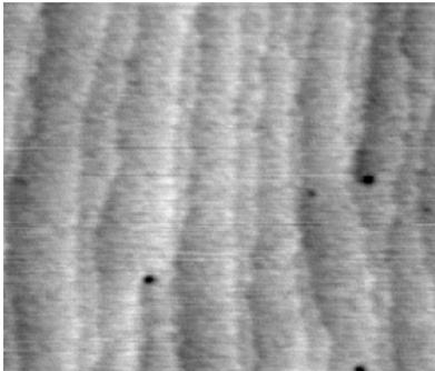
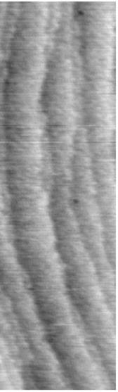
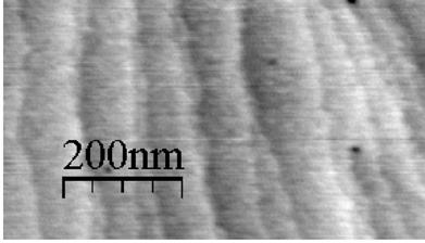
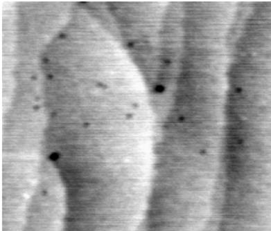
2 Dislocation density-dependent quality factors in InGaN quantum dot containing microdisks H.A.R. El-Ella a), M.J. Kappers, R.A.Oliver Department of Materials Science and Metallurgy, University of Cambridge, Pembroke Street, Cambridge CB2 3QZ, UK F. Rol, K. Russell, E.L. Hu School of Engineering and Applied Sciences, Harvard University, Oxford Street, Cambridge MA 02138, USA Microdisks incorporating InGaN quantum dots were fabricated using SiO 2 microspheres as a hard mask in conjunction with a photoelectrochemical etch step from a structure containing a sacrificial InGaN/InGaN super-lattice. Formation of microdisks from two near-identical structures with differing dislocation densities was carried out and investigated using micro-photoluminescence. This confirmed the existence of quantum dots through the presence of resolution limited spectral lines and showed a clear correlation between the resulting modes quality factors and the dislocation densities within the disks. The disks with higher dislocation densities showed up to 80% lower quality factors than the low dislocation density disks. There has been much recent progress in the demonstration of cavity quantum electrodynamics (CQED) in the solid state using modal engineering of high quality optical cavities to dramatically alter the optical behaviour of emitters embedded within. Weak coupling of emitter and cavity can produce controlled single photon emission and ultra-low threshold optical sources 1,2,3, while in the limit of strong emitter-cavity coupling new quantum mechanical states have been observed 4,5,6,7 that could serve as the basis for quantum information processing 8. Although CQED has been explored in a variety of semiconductor materials, there has been relatively little application to the III-nitrides, although their high-band gaps, large exciton binding energies and possible room temperature implementation of CQED effects provide strong motivation to do so 9. InGaN quantum wells (QW) have been incorporated as the active layers within microdisks 10 and photonic crystals 11 ; generally the Q s (Q = λ δλ ) of these microcavities have been modest (~4000), although low threshold lasing has been observed in microdisks 12. The incorporation of quantum dot (QD) active layers promises lower re-absorption (hence loss) than for QW structures, and thus the possibility of achieving higher quality emitter-cavity coupling 13. InGaN QD active layers have thus far only been reported within pillar cavities with a reported Q not exceeding Efforts to explore other geometries, such as microdisks and photonic crystals, encounter the challenges of obtaining high quality InGaN QDs in heterostructures that have also been designed to allow sufficient optical isolation of the cavities. This paper reports the successful growth and fabrication of InGaN QD-containing microdisks and highlights a correlation between the material quality (dislocation density) and the obtained average Q values. Microdisks were fabricated through a band gap selective photoelectrochemical etch (PECE) in conjunction with a sacrificial super-lattice (SSL), from structures grown on 2 in. c-plane GaN/Al 2O 3 pseudo-substrates by metalorganic vapour phase epitaxy (the pseudo-substrate growth method is described in Ref. 15). The structure design is intended for the creation of undercut microdisks, and consists of an In xga 1-xN/In yga 1-yN SSL grown on an n-doped GaN pseudo-substrate, capped by a thin (~10 nm) layer of GaN followed by an Al 0.19Ga 0.81N etch stop layer and a GaN membrane containing an InGaN a) Electronic mail: he234@cam.ac.uk 1
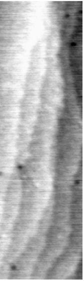
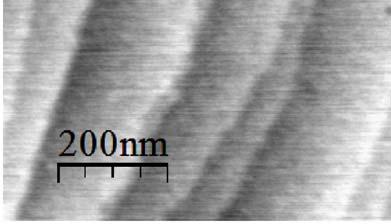
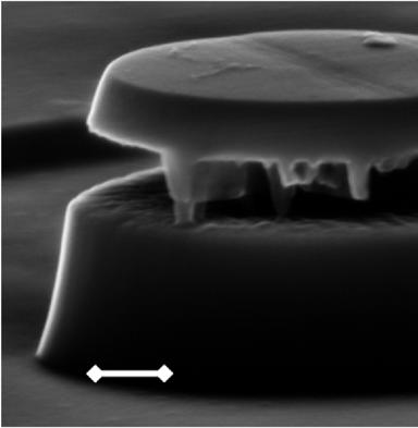
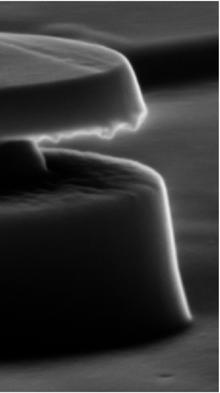
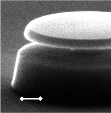
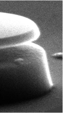
3 QD layer. As there is a strong inherent polarization in c-plane nitrides, the super-lattice is intended to modulate the bandedge and ensure a homogenous distribution of photogenerated holes across the SSL surface during the PECE process. The In 0.2Ga 0.8N QD layer was grown through a self-assembled droplet epitaxy method which is described in more detail in Ref. 16. The In content of this QD layer is nominally 20%, but usually varies throughout the layer. The QD-containing microdisk consists of all the layers above the SSL, which serves as the post. A GaN layer was grown between the AlGaN and SSL in order to protect the InGaN SSL layers from the temperature ramp required prior to the AlGaN growth. Two structures containing different SSL In contents were used for fabrication with x/y ~ 7%/11% (structure A) and ~ 5%/7% (structure B). These two structures were grown in order to explore the extent of strain-relaxation and resulting material quality throughout the structure and on the fabricated microdisks. The dislocation density (DD) of both sample A and B (table I) was determined through calculating the surface pit density (figure 1) using atomic force microscopy (AFM), in combination with cross sectional transmission electron microscopy. These techniques highlighted the generation of additional dislocations within structure A due to strain-relaxation resulting from an over-abundance of In in the SSL. A student t-test verified the statistical significance (p<0.002) of a larger DD in A (~ cm -2 ) to that in B (~ cm -2 ). Fabrication of microdisks with a diameter of ~1.1 μm was carried out by first depositing a protective 5 nm SiO 2 layer on the full structure and dispersing 1 μm diameter SiO 2 spheres onto its surface. The spheres formed masks for an inductivelycoupled plasma etch in Cl 2/N 2 that transferred the pattern ~1.5 μm into the full structure, stopping in the GaN pseudosubstrate. Subsequent immersion in 50% HF removed the masking layer. Contact lithography was then employed to deposit a Ti/Pt cathode grid onto the surface. The resulting mesas were then partially undercut by selectively etching the SSL in 2.4 mm HCl using PECE (details of the full PECE procedure can be found in Ref. 10). Micro-photoluminescence (μpl) of the microdisks was carried out between room temperature (RT) and 5 K using a pulsed frequency-doubled Ti-sapphire laser emitting at 360 nm. The laser was passed through a variable-neutral density filter and focused by a microscope objective (numerical aperture = 0.5) to a spot diameter of ~1 μm. The objective was mounted on a xyz piezoelectric stage with a spatial positioning accuracy of ~5 nm. The vertical emission of microdisks was then collected by the same objective, dispersed through to a 0.5 m focal length spectrometer with a 1200 lmm -1 diffraction grating and collected by a liquid N 2 cooled charge coupled device. The microdisks were placed on a cold-finger helium flow cryostat that was mounted on an electronically controlled xy linear translational stage with a spatial positioning accuracy of ~50 nm. Figure 2 shows μpl spectra from a disk fabricated from material B at 150 K and at 5 K, highlighting modes with a spacing of λ ~24 nm and the presence of resolution limited peaks originating from the InGaN QDs. The measured mode spacing correlates well with the theoretical mode spacing of the lowest radial order whispering gallery mode Δ =, with n eff = 2.5 and r = 550 nm) indicating the absence of higher radial order modes and the ( λ = n λ rπneff excellent circularity resulting from the fabrication process. Scanning electron microscopy (SEM) images of sample microdisks created from both A and B are shown in figure 3 along with a sample μpl scan from each taken at RT. Microdisks fabricated from material A were observed to exhibit a larger density of whiskers protruding from the disk periphery and underside (in some cases extending as far as the base), reflecting the larger DD. Serving as traps for the photogenerated carriers, and thus locally reducing the etch rate, these dislocations become decorated during the etch, forming whiskers 17. Direct observation in the SEM of microdisks with 300 nm undercuts showed that 9 out of 10 disks created from structure A exhibited whiskers, compared to only 2 out of 10 from structure B. Measured Q values of microdisks from both samples (figure 4) revealed a larger average value obtained from those of structure B. The difference in mean Q values between A and B was verified to be statistically significant through a student t- test (p<10-4 ) with A and B exhibiting a mean Q of ~2000 and ~600 respectively (with a standard deviation of ~450 and 2
4 ~145 respectively, see table 1). While there are a multitude of possible reasons and mechanisms that can limit measured Q s, the measured differences in the controlled comparison of microdisks from A and B are well accounted for as there is a clear statistical correlation between the DD, the number of observed disks displaying whiskers, and the measured Q values. This strongly suggests that the difference in the Q values is a result of the material DD (and therefore material quality). However, the mechanism by which these dislocations degrade the Q values is not clear and needs to be investigated further. In particular, it is difficult to pinpoint due to the possibility of several competing scattering and absorption lossmechanisms attributed to the dislocations themselves. Possible loss mechanisms include scattering from the whiskers, although it is not obvious if this is due to the protruding whiskers themselves or through the possible large scale surface roughness their presence causes. The large surface-volume ratio would also possibly enhance the sensitivity to such surface irregularities as has been often shown in other systems 18,19. The DD within the microdisk itself may also have a significant contribution to sub-bandgap absorption due to band-bending and expected defect level traps occurring within the bandgap. Less obvious mechanisms such as absorption and scattering within the QD active layer in the presence of an increased DD must also be contemplated and studied, especially considering the fluctuation of In around dislocations as well as the growth method and irregularity of the InGaN QD layer. (As well as a broad QD size and composition distribution, modified droplet epitaxy results in a fragmented underlying QW layer and a large density of irregular features with dimensions similar or larger than that of the confined light). To summarise, microdisks containing In 0.2Ga 0.8N QDs were fabricated via a selective PECE process from two structures with differing dislocation densities. μpl of microdisks created from both low and high dislocation density material showed a striking correlation between the Q factors and the dislocation density, with the lower dislocation density material exhibiting higher Q factors. Further study is required, as well as optimization of the cavity structure, in order to measure the degree of scattering- and absorption-based mechanisms attributed to the dislocations themselves (both the protruding whiskers and within the microdisk), and assess their contribution to the overall cavity loss. We believe that this study provides important insights into the influence of the material quality on cavity performance in these materials. These insights are critical in enabling the further integrated optimization of material and cavity design to achieve strong QD-cavity coupling. This work was supported in part by the NSF Materials World Network (award no ), the Engineering and Physical Sciences Research Council and the Royal Academy of Engineering. R.A. Oliver would like to acknowledge funding from the Royal Society. Figure Captions: Figure 1: Figure 2: Figure 3: Figure 4: 1 μm 1 μm AFM scans of (a) structure A, (b) structure B showing surface pits associated with threading dislocations. μpl spectra collected vertically from a μdisk fabricated from material B at (a) 150 K and (b) 5 K, with the modes shaded. Sample SEM images and RT μpl spectra collected from (a,i,ii) material A and (b,i,ii) material B (inset graphs show Lorentzian fits of the respective modes). Note that (b,i) was tilted at a different angle to (a,i), thereby projecting an image of a thinner disk. Measured Q values from eight observed modes of μdisks fabricated from structure A ( ) and structure B ( ). 3
5 Table I: Structure In % in SSL Surface Pit Density (cm -2 ) Q σ(q) A 6.7% / 10.7% ~ (3 ± 0.4) 10 9 ~ 600 ± 50 ~145 B 5.1% / 6.5% ~ (7 ± 0.7) 10 8 ~ 2000 ± 160 ~450 Table I caption: Summary of compositions, pit densities and average Q (both with standard error), as well as the standard deviation(σ) of the measured Q from eight observed modes shown in figure 4. References 1 P. Michler, A. Kiraz, C. Becher, W.V. Schoenfeld, P.M. Petroff, L. Zhang, E.L. Hu and A. Imamoğlu, Science 290, 2282 (2000) 2 K. Srinivasan, M. Borselli, T.J. Johnson, P.E. Barclay, O. Painter, A. Stintz and S. Krishna, Appl. Phys. Lett. 86, (2005) 3 W.-H. Chang, W.-Y. Chen, H.-S. Chang, T.-P. Hsieh, J.-I. Chyi and T.-M. Hsu, Phys. Rev. Lett. 96, (2006) 4 J.P. Reithmaier, G. SęK, A. Löffler, C. Hofmann, S. Kuhn, S Reitzenstein, L.V. Keldysh, V.D. Kulakovskii, T.L. Reinecke and A. Forchel Nature (London) 432, 197 (2004). 5 T.Yoshie, A. Scherer, J. Hendrickson, G. Khitrova, H.M. Gibbs, G. Rupper, C. Ell, O.B. Shchekin and D.G. Deppe Nature (London) 432, 200 (2004) 6 E. Peter, P. Snellart, D. Martou, A. Lemaître, J. Hours, J.M. Gérard and J. Bloch Phys, Rev. Lett. 95, (2005) 7 K. Hennessy, A. Badolato, M. Winger, D. Gerave, M. Atatüre, S. Gulde, S. Fält, E.L. Hu and A. Imamoğlu, Nature (London) 445, 896 (2007) 8 A. Imamoğlu, D.D. Awschalom, G. Burkard, D.P. DiVincenzo, D. Loss, M. Sherwin and A. Small, Phys. Rev. Lett, 83, 4204 (1999) 9 G. Christmann, R. Butté, E.Feltin, A. Mouti, P. A. Stadelmann, A. Castiglia, J.-F. Carlin, and N. Grandjean, Phys. Rev. B 77, (2008) 10 E.D. Haberer, R. Sharma, C. Meier, A.R. Stonas, S. Nakamura, S.P. DenBaars, E.L. Hu, Appl. Phys. Lett (2004) 11 Y.-S. Choi, C. Meier, K. Hennessy, R. Sharma, E. Haberer, Y. Gao, S. P. DenBaars, S. Nakamura, and E. L. Hu, Appl. Phys. Lett. 87, (2005) 12 A.C. Tamboli, E.D. Haberer, R. Sharma, K.H. Lee, S. Nakamura and E.L. Hu, Nature Photonics (London) 1, 61 (2007) 13 B. Gayral, J. M. Gérard, A. Lemaître, C. Dupuis, L. Manin, and J. L. Pelouard Appl. Phys. Lett., 75, 1908 (1999) 14 K. Sebald, M. Seyfried, J. Kalden, J. Gutowski, H. Dartsch, C. Tessarek, T. Aschenbrenner, S. Figge, C. Kruse, D. Hommel, M. Florian, and F. Jahnke Appl. Phys. Lett. 96, (2010) 15 R.A. Oliver, M.J. Kappers, J. Sumner, R. Datta, C.J. Humphreys, J. Cryst. Growth (2006) 16 R.A. Oliver, G.A.D. Briggs, M.J. Kappers. C.J. Humphreys, S. Yasin, J.H. Rice, J.D Smith, R.A. Taylor Appl. Phys. Lett., (2003) 17 C. Youtsey, L.T. Romano and I. Adesida, Appl. Phys. Lett. 73, 797 (1998) 18 R. D. Kekatpure, M. L. Brongersma, Phys Rev A, 78, (2008) 19 C.P. Michael, K. Srinivasan, T.J. Johnson, O. Painter, K.H.Lee, K. Hennessy, E.L. Hu, Appl. Phys Lett, 90, (2007) 4
6
7
8
9
Controlled Tuning of Whispering Gallery Modes of GaN/InGaN Microdisk Cavities
 Controlled Tuning of Whispering Gallery Modes of GaN/InGaN Microdisk Cavities The Harvard community has made this article openly available. Please share how this access benefits you. Your story matters.
A full free spectral range tuning of p-i-n doped Gallium Nitride
 A full free spectral range tuning of p-i-n doped Gallium Nitride microdisk cavity Nan Niu 1, Tsung-Li Liu 1, Igor Aharonovich 1, Kasey J Russell 1, Alexander Woolf 1, Thomas C. Sadler 2, Haitham A.R. El-Ella
Low threshold, room-temperature microdisk lasers in the blue spectral range
 Low threshold, room-temperature microdisk lasers in the blue spectral range Igor Aharonovich*,(a)1, Alexander Woolf* 1, Kasey J. Russell 1 *, Tongtong Zhu 2, Menno J. Kappers 2, Rachel A. Oliver 2 and
Quantum Dot Lasers Using High-Q Microdisk Cavities
 phys. stat. sol. (b) 224, No. 3, 797 801 (2001) Quantum Dot Lasers Using High-Q Microdisk Cavities P. Michler 1; *Þ (a), A. Kiraz (a), C. Becher (a), Lidong Zhang (a), E. Hu (a), A. Imamoglu (a), W. V.
Single-photon nonlinearity of a semiconductor quantum dot in a cavity
 Single-photon nonlinearity of a semiconductor quantum dot in a cavity D. Sanvitto, F. P. Laussy, F. Bello, D. M. Whittaker, A. M. Fox and M. S. Skolnick Department of Physics and Astronomy, University
Room temperature continuous wave lasing in InAs quantum-dot microdisks with air cladding
 Room temperature continuous wave lasing in InAs quantum-dot microdisks with air cladding Toshihide Ide and Toshihiko Baba Yokohama National University, Department of Electrical and Computer Engineering
Strongly coupled single quantum dot in a photonic crystal waveguide cavity
 Strongly coupled single quantum dot in a photonic crystal waveguide cavity F.S.F. Brossard 1*, X. L. Xu 1*, D.A. Williams 1, M. Hadjipanayi 2, M. Hopkinson 3, X. Wang 2 and R.A. Taylor 2 1 Hitachi Cambridge
Fabrication of Efficient Blue Light-Emitting Diodes with InGaN/GaN Triangular Multiple Quantum Wells. Abstract
 Fabrication of Efficient Blue Light-Emitting Diodes with InGaN/GaN Triangular Multiple Quantum Wells R. J. Choi, H. W. Shim 2, E. K. Suh 2, H. J. Lee 2, and Y. B. Hahn,2, *. School of Chemical Engineering
Air-holes radius change effects and structure transitions in the linear photonic crystal nanocavities
 American Journal of Optics and Photonics 2013; 1(3): 11-16 Published online June 20, 2013 (http://www.sciencepublishinggroup.com/j/ajop) doi: 10.11648/j.ajop.20130103.11 Air-holes radius change effects
Fabrication-tolerant high quality factor photonic crystal microcavities
 Fabrication-tolerant high quality factor photonic crystal microcavities Kartik Srinivasan, Paul E. Barclay, and Oskar Painter Department of Applied Physics, California Institute of Technology, Pasadena,
Low threshold and room-temperature lasing of electrically pumped red-emitting InP/(Al Ga 0.80 ) In 0.49.
 In 0.49.") Journal of Physics: Conference Series Low threshold and room-temperature lasing of electrically pumped red-emitting InP/(Al 0.20 Ga 0.80 ) 0.51 In 0.49 P quantum dots To cite this article: Marcus Eichfelder
Journal of Physics: Conference Series Low threshold and room-temperature lasing of electrically pumped red-emitting InP/(Al 0.20 Ga 0.80 ) 0.51 In 0.49 P quantum dots To cite this article: Marcus Eichfelder
Continuous room-temperature operation of optically pumped InGaAs/InGaAsP microdisk lasers
 Continuous room-temperature operation of optically pumped InGaAs/InGaAsP microdisk lasers S. M. K. Thiyagarajan, A. F. J. Levi, C. K. Lin, I. Kim, P. D. Dapkus, and S. J. Pearton + Department of Electrical
Photoluminescence experiment on quantum dots embedded in a large Purcell-factor microcavity
 PHYSICAL REVIEW B 78, 235306 2008 Photoluminescence experiment on quantum dots embedded in a large Purcell-factor microcavity B. Gayral and J. M. Gérard CEA-CNRS Group Nanophysique et Semiconducteurs,
Supplementary Information for
 Supplementary Information for Multi-quantum well nanowire heterostructures for wavelength-controlled lasers Fang Qian 1, Yat Li 1 *, Silvija Gradečak 1, Hong-Gyu Park 1, Yajie Dong 1, Yong Ding 2, Zhong
Ultrafast single photon emitting quantum photonic structures. based on a nano-obelisk
 Ultrafast single photon emitting quantum photonic structures based on a nano-obelisk Je-Hyung Kim, Young-Ho Ko, Su-Hyun Gong, Suk-Min Ko, Yong-Hoon Cho Department of Physics, Graduate School of Nanoscience
Wavelength extension of GaInAs/GaIn(N)As quantum dot structures grown on GaAs
As quantum dot structures grown on GaAs") PUBLICATION V Journal of Crystal Growth 248 (2003) 339 342 Wavelength extension of GaInAs/GaIn(N)As quantum dot structures grown on GaAs T. Hakkarainen*, J. Toivonen, M. Sopanen, H. Lipsanen Optoelectronics
PUBLICATION V Journal of Crystal Growth 248 (2003) 339 342 Wavelength extension of GaInAs/GaIn(N)As quantum dot structures grown on GaAs T. Hakkarainen*, J. Toivonen, M. Sopanen, H. Lipsanen Optoelectronics
Photonic Crystal Nanocavities for Efficient Light Confinement and Emission
 Journal of the Korean Physical Society, Vol. 42, No., February 2003, pp. 768 773 Photonic Crystal Nanocavities for Efficient Light Confinement and Emission Axel Scherer, T. Yoshie, M. Lončar, J. Vučković
Contents Part I Concepts 1 The History of Heterostructure Lasers 2 Stress-Engineered Quantum Dots: Nature s Way
 Contents Part I Concepts 1 The History of Heterostructure Lasers Zhores I. Alferov... 3 1.1 Introduction... 3 1.2 The DHS Concept and Its Application for Semiconductor Lasers. 3 1.3 Quantum Dot Heterostructure
Investigation on Mode Splitting and Degeneracy in the L3 Photonic Crystal Nanocavity via Unsymmetrical Displacement of Air-Holes
 The International Journal Of Engineering And Science (Ijes) Volume 2 Issue 2 Pages 146-150 2013 Issn: 2319 1813 Isbn: 2319 1805 Investigation on Mode Splitting and Degeneracy in the L3 Photonic Crystal
SUPPLEMENTARY INFORMATION
 doi:10.1038/nature12036 We provide in the following additional experimental data and details on our demonstration of an electrically pumped exciton-polariton laser by supplementing optical and electrical
Temperature Dependence of Photoluminescence from Epitaxial InGaAs/GaAs Quantum Dots with High Lateral Aspect Ratio
 Vol. 120 (2011) ACTA PHYSICA POLONICA A No. 5 40th Jaszowiec International School and Conference on the Physics of Semiconductors, Krynica-Zdrój 2011 Temperature Dependence of Photoluminescence from Epitaxial
Determining the Elastic Modulus and Hardness of an Ultrathin Film on a Substrate Using Nanoindentation
 Determining the Elastic Modulus and Hardness of an Ultrathin Film on a Substrate Using Nanoindentation The Harvard community has made this article openly available. Please share how this access benefits
Photonic devices for quantum information processing:
 Outline Photonic devices for quantum information processing: coupling to dots, structure design and fabrication Optoelectronics Group, Cavendish Lab Outline Vuckovic s group Noda s group Outline Outline
Supplementary Information Our InGaN/GaN multiple quantum wells (MQWs) based one-dimensional (1D) grating structures
 based one-dimensional (1D) grating structures") Polarized white light from hybrid organic/iii-nitrides grating structures M. Athanasiou, R. M. Smith, S. Ghataora and T. Wang* Department of Electronic and Electrical Engineering, University of Sheffield,
Polarized white light from hybrid organic/iii-nitrides grating structures M. Athanasiou, R. M. Smith, S. Ghataora and T. Wang* Department of Electronic and Electrical Engineering, University of Sheffield,
Self-Assembled InAs Quantum Dots
 Self-Assembled InAs Quantum Dots Steve Lyon Department of Electrical Engineering What are semiconductors What are semiconductor quantum dots How do we make (grow) InAs dots What are some of the properties
Temperature Dependent Optical Band Gap Measurements of III-V films by Low Temperature Photoluminescence Spectroscopy
 Temperature Dependent Optical Band Gap Measurements of III-V films by Low Temperature Photoluminescence Spectroscopy Linda M. Casson, Francis Ndi and Eric Teboul HORIBA Scientific, 3880 Park Avenue, Edison,
Exciton photon strong-coupling regime for a single quantum dot in a microcavity.
 Exciton photon strong-coupling regime for a single quantum dot in a microcavity. Emmanuelle Peter, Pascale Senellart, David Martrou, Aristide Lemaître, Jacqueline Bloch, Julien Hours, Jean-Michel Gérard
III-V nanostructured materials synthesized by MBE droplet epitaxy
 III-V nanostructured materials synthesized by MBE droplet epitaxy E.A. Anyebe 1, C. C. Yu 1, Q. Zhuang 1,*, B. Robinson 1, O Kolosov 1, V. Fal ko 1, R. Young 1, M Hayne 1, A. Sanchez 2, D. Hynes 2, and
arxiv: v2 [physics.optics] 8 Nov 2013
![arxiv: v2 [physics.optics] 8 Nov 2013](/thumbs/80/80705215.jpg "arxiv: v2 [physics.optics] 8 Nov 2013") Single Photon Emission from Site-Controlled InGaN/GaN Quantum Dots Lei Zhang, Tyler A. Hill, and Hui Deng Department of Physics, University of Michigan, 450 Church Street, Ann Arbor, MI 48109, USA Chu-Hsiang
Single Photon Emission from Site-Controlled InGaN/GaN Quantum Dots Lei Zhang, Tyler A. Hill, and Hui Deng Department of Physics, University of Michigan, 450 Church Street, Ann Arbor, MI 48109, USA Chu-Hsiang
Room-temperature continuous-wave operation of GaInNAs/GaAs quantum dot laser with GaAsN barrier grown by solid source molecular beam epitaxy
 Room-temperature continuous-wave operation of GaInNAs/GaAs quantum dot laser with GaAsN barrier grown by solid source molecular beam epitaxy Z. Z. Sun 1, S. F. Yoon 1,2, K. C. Yew 1, and B. X. Bo 1 1 School
Emission Spectra of the typical DH laser
 Emission Spectra of the typical DH laser Emission spectra of a perfect laser above the threshold, the laser may approach near-perfect monochromatic emission with a spectra width in the order of 1 to 10
Nanomaterials and their Optical Applications
 Nanomaterials and their Optical Applications Winter Semester 2012 Lecture 08 rachel.grange@uni-jena.de http://www.iap.uni-jena.de/multiphoton Outline: Photonic crystals 2 1. Photonic crystals vs electronic
Abnormal PL spectrum in InGaN MQW surface emitting cavity
 Abnormal PL spectrum in InGaN MQW surface emitting cavity J. T. Chu a, Y.-J. Cheng b, H. C. Kuo a, T. C. Lu a, and S. C. Wang a a Department of Photonics & Institute of Electro-Optical Engineering, National
Wavelength Stabilized High-Power Quantum Dot Lasers
 Wavelength Stabilized High-Power Quantum Dot Lasers Johann Peter Reithmaier Technische Physik, Institute of Nanostructure Technologies & Analytics () Universität Kassel, Germany W. Kaiser, R. Debusmann,
Part I. Nanostructure design and structural properties of epitaxially grown quantum dots and nanowires
 Part I Nanostructure design and structural properties of epitaxially grown quantum dots and nanowires 1 Growth of III V semiconductor quantum dots C. Schneider, S. Höfling and A. Forchel 1.1 Introduction
Single Semiconductor Nanostructures for Quantum Photonics Applications: A solid-state cavity-qed system with semiconductor quantum dots
 The 3 rd GCOE Symposium 2/17-19, 19, 2011 Tohoku University, Sendai, Japan Single Semiconductor Nanostructures for Quantum Photonics Applications: A solid-state cavity-qed system with semiconductor quantum
Optical and Terahertz Characterization of Be-Doped GaAs/AlAs Multiple Quantum Wells
 Vol. 107 (2005) ACTA PHYSICA POLONICA A No. 2 Proceedings of the 12th International Symposium UFPS, Vilnius, Lithuania 2004 Optical and Terahertz Characterization of Be-Doped GaAs/AlAs Multiple Quantum
Semiconductor Disk Laser on Microchannel Cooler
 Semiconductor Disk Laser on Microchannel Cooler Eckart Gerster An optically pumped semiconductor disk laser with a double-band Bragg reflector mirror is presented. This mirror not only reflects the laser
Photoluminescence characterization of quantum dot laser epitaxy
 Photoluminescence characterization of quantum dot laser epitaxy Y. Li *, Y. C. Xin, H. Su and L. F. Lester Center for High Technology Materials, University of New Mexico 1313 Goddard SE, Albuquerque, NM
Spin selective Purcell effect in a quantum dot microcavity system
 Spin selective urcell effect in a quantum dot microcavity system Qijun Ren, 1 Jian Lu, 1, H. H. Tan, 2 Shan Wu, 3 Liaoxin Sun, 1 Weihang Zhou, 1 Wei ie, 1 Zheng Sun, 1 Yongyuan Zhu, 3 C. Jagadish, 2 S.
Luminescence basics. Slide # 1
 Luminescence basics Types of luminescence Cathodoluminescence: Luminescence due to recombination of EHPs created by energetic electrons. Example: CL mapping system Photoluminescence: Luminescence due to
Investigation of Optical Nonlinearities and Carrier Dynamics in In-Rich InGaN Alloys
 Vol. 113 (2008) ACTA PHYSICA POLONICA A No. 3 Proceedings of the 13th International Symposium UFPS, Vilnius, Lithuania 2007 Investigation of Optical Nonlinearities and Carrier Dynamics in In-Rich InGaN
arxiv:quant-ph/ v3 20 Apr 2005
 Controlling the Spontaneous Emission Rate of Single Quantum Dots in a 2D Photonic Crystal Dirk Englund, 1 David Fattal, 1 Edo Waks, 1 Glenn Solomon, 1,2 Bingyang Zhang, 1 Toshihiro Nakaoka, 3 Yasuhiko
Optical Loss and Lasing Characteristics of AlGaAs Microdisk Cavities with Embedded Quantum Dots
 167 Chapter 5 Optical Loss and Lasing Characteristics of AlGaAs Microdisk Cavities with Embedded Quantum Dots 5.1 Introduction For future experiments in cavity QED with self-assembled quantum dots, the
Supplementary Figure 1 Comparison of single quantum emitters on two type of substrates:
 Supplementary Figure 1 Comparison of single quantum emitters on two type of substrates: a, Photoluminescence (PL) spectrum of localized excitons in a WSe 2 monolayer, exfoliated onto a SiO 2 /Si substrate
Supplementary Figure S1. AFM characterizations and topographical defects of h- BN films on silica substrates. (a) (c) show the AFM height
 (c) show the AFM height") Supplementary Figure S1. AFM characterizations and topographical defects of h- BN films on silica substrates. (a) (c) show the AFM height topographies of h-bn film in a size of ~1.5µm 1.5µm, 30µm 30µm
Supplementary Figure S1. AFM characterizations and topographical defects of h- BN films on silica substrates. (a) (c) show the AFM height topographies of h-bn film in a size of ~1.5µm 1.5µm, 30µm 30µm
Ultrafast All-optical Switches Based on Intersubband Transitions in GaN/AlN Multiple Quantum Wells for Tb/s Operation
 Ultrafast All-optical Switches Based on Intersubband Transitions in GaN/AlN Multiple Quantum Wells for Tb/s Operation Jahan M. Dawlaty, Farhan Rana and William J. Schaff Department of Electrical and Computer
Optical Investigation of the Localization Effect in the Quantum Well Structures
 Department of Physics Shahrood University of Technology Optical Investigation of the Localization Effect in the Quantum Well Structures Hamid Haratizadeh hamid.haratizadeh@gmail.com IPM, SCHOOL OF PHYSICS,
(Al,In)GaN laser diodes in spectral, spatial, and time domain: near-field measurements and basic simulations
GaN laser diodes in spectral, spatial, and time domain: near-field measurements and basic simulations") (Al,In)GaN laser diodes in spectral, spatial, and time domain: near-field measurements and basic simulations Ulrich Schwarz Department of Experimental and Applied Physics Regensburg University Optical
(Al,In)GaN laser diodes in spectral, spatial, and time domain: near-field measurements and basic simulations Ulrich Schwarz Department of Experimental and Applied Physics Regensburg University Optical
Widely Tunable and Intense Mid-Infrared PL Emission from Epitaxial Pb(Sr)Te Quantum Dots in a CdTe Matrix
Te Quantum Dots in a CdTe Matrix") Widely Tunable and Intense Mid-Infrared PL Emission from Epitaxial Pb(Sr)Te Quantum Dots in a Matrix S. Kriechbaumer 1, T. Schwarzl 1, H. Groiss 1, W. Heiss 1, F. Schäffler 1,T. Wojtowicz 2, K. Koike 3,
Widely Tunable and Intense Mid-Infrared PL Emission from Epitaxial Pb(Sr)Te Quantum Dots in a Matrix S. Kriechbaumer 1, T. Schwarzl 1, H. Groiss 1, W. Heiss 1, F. Schäffler 1,T. Wojtowicz 2, K. Koike 3,
Polariton laser in micropillar cavities
 Polariton laser in micropillar cavities D. Bajoni, E. Wertz, P. Senellart, I. Sagnes, S. Bouchoule, A. Miard, E. Semenova, A. Lemaître and J. Bloch Laboratoire de Photonique et de Nanostructures LPN/CNRS,
ANTIMONY ENHANCED HOMOGENEOUS NITROGEN INCORPORATION INTO GaInNAs FILMS GROWN BY ATOMIC HYDROGEN-ASSISTED MOLECULAR BEAM EPITAXY
 ANTIMONY ENHANCED HOMOGENEOUS NITROGEN INCORPORATION INTO GaInNAs FILMS GROWN BY ATOMIC HYDROGEN-ASSISTED MOLECULAR BEAM EPITAXY Naoya Miyashita 1, Nazmul Ahsan 1, and Yoshitaka Okada 1,2 1. Research Center
Resonantly Excited Time-Resolved Photoluminescence Study of Self-Organized InGaAs/GaAs Quantum Dots
 R. Heitz et al.: PL Study of Self-Organized InGaAs/GaAs Quantum Dots 65 phys. stat. sol. b) 221, 65 2000) Subject classification: 73.61.Ey; 78.47.+p; 78.55.Cr; 78.66.Fd; S7.12 Resonantly Excited Time-Resolved
interband transitions in semiconductors M. Fox, Optical Properties of Solids, Oxford Master Series in Condensed Matter Physics
 interband transitions in semiconductors M. Fox, Optical Properties of Solids, Oxford Master Series in Condensed Matter Physics interband transitions in quantum wells Atomic wavefunction of carriers in
Loss of Quantum Efficiency in Green Light Emitting Diode Dies at Low Temperature
 Mater. Res. Soc. Symp. Proc. Vol. 955 2007 Materials Research Society 0955-I15-12 Loss of Quantum Efficiency in Green Light Emitting Diode Dies at Low Temperature Yufeng Li 1,2, Wei Zhao 1,2, Yong Xia
Appendix. Photonic crystal lasers: future integrated devices
 91 Appendix Photonic crystal lasers: future integrated devices 5.1 Introduction The technology of photonic crystals has produced a large variety of new devices. However, photonic crystals have not been
Electron leakage effects on GaN-based light-emitting diodes
 Opt Quant Electron (2010) 42:89 95 DOI 10.1007/s11082-011-9437-z Electron leakage effects on GaN-based light-emitting diodes Joachim Piprek Simon Li Received: 22 September 2010 / Accepted: 9 January 2011
EV Group. Engineered Substrates for future compound semiconductor devices
 EV Group Engineered Substrates for future compound semiconductor devices Engineered Substrates HB-LED: Engineered growth substrates GaN / GaP layer transfer Mobility enhancement solutions: III-Vs to silicon
Progress Report to AOARD
 Progress Report to AOARD C. C. (Chih-Chung) Yang The Graduate Institute of Electro-Optical Engineering National Taiwan University No. 1, Roosevelt Road, Section 4, Taipei, Taiwan (phone) 886-2-23657624
Exploiting pattern transformation to tune phononic band gaps in a two-dimensional granular crystal
 Exploiting pattern transformation to tune phononic band gaps in a two-dimensional granular crystal The Harvard community has made this article openly available. Please share how this access benefits you.
1 Semiconductor Quantum Dots for Ultrafast Optoelectronics
 j1 1 Semiconductor Quantum Dots for Ultrafast Optoelectronics 1.1 The Role of Dimensionality in Semiconductor Materials The history of semiconductor lasers has been punctuated by dramatic revolutions.
Raman spectroscopy of self-assembled InAs quantum dots in wide-bandgap matrices of AlAs and aluminium oxide
 Mat. Res. Soc. Symp. Proc. Vol. 737 2003 Materials Research Society E13.8.1 Raman spectroscopy of self-assembled InAs quantum dots in wide-bandgap matrices of AlAs and aluminium oxide D. A. Tenne, A. G.
2D MBE Activities in Sheffield. I. Farrer, J. Heffernan Electronic and Electrical Engineering The University of Sheffield
 2D MBE Activities in Sheffield I. Farrer, J. Heffernan Electronic and Electrical Engineering The University of Sheffield Outline Motivation Van der Waals crystals The Transition Metal Di-Chalcogenides
Enhancing the Rate of Spontaneous Emission in Active Core-Shell Nanowire Resonators
 Chapter 6 Enhancing the Rate of Spontaneous Emission in Active Core-Shell Nanowire Resonators 6.1 Introduction Researchers have devoted considerable effort to enhancing light emission from semiconductors
Nanocomposite photonic crystal devices
 Nanocomposite photonic crystal devices Xiaoyong Hu, Cuicui Lu, Yulan Fu, Yu Zhu, Yingbo Zhang, Hong Yang, Qihuang Gong Department of Physics, Peking University, Beijing, P. R. China Contents Motivation
Simulation of GaN-based Light-Emitting Devices
 Simulation of GaN-based Light-Emitting Devices Joachim Piprek Solid-State Lighting and Display Center Materials Department, College of Engineering University of California, Santa Barbara, CA 93106 piprek@ieee.org
Segmented 1.55um Laser with 400% Differential Quantum Efficiency J. Getty, E. Skogen, L. Coldren, University of California, Santa Barbara, CA.
 Segmented 1.55um Laser with 400% Differential Quantum Efficiency J. Getty, E. Skogen, L. Coldren, University of California, Santa Barbara, CA. Abstract: By electrically segmenting, and series-connecting
Electronic States of InAs/GaAs Quantum Dots by Scanning Tunneling Spectroscopy
 Electronic States of InAs/GaAs Quantum Dots by Scanning Tunneling Spectroscopy S. Gaan, Guowei He, and R. M. Feenstra Dept. Physics, Carnegie Mellon University, Pittsburgh, PA 15213 J. Walker and E. Towe
Influence of excitation frequency on Raman modes of In 1-x Ga x N thin films
 Influence of excitation frequency on Raman modes of In 1-x Ga x N thin films A. Dixit 1,, J. S. Thakur 2, V. M. Naik 3, R. Naik 2 1 Center of Excellence in Energy & ICT, Indian Institute of Technology
InAs Quantum Dots for Quantum Information Processing
 InAs Quantum Dots for Quantum Information Processing Xiulai Xu 1, D. A. Williams 2, J. R. A. Cleaver 1, Debao Zhou 3, and Colin Stanley 3 1 Microelectronics Research Centre, Cavendish Laboratory, University
Mapping the potential within a nanoscale undoped GaAs region using. a scanning electron microscope
 Mapping the potential within a nanoscale undoped GaAs region using a scanning electron microscope B. Kaestner Microelectronics Research Centre, Cavendish Laboratory, University of Cambridge, Madingley
Optical Gain Analysis of Strain Compensated InGaN- AlGaN Quantum Well Active Region for Lasers Emitting at nm
 Optical Gain Analysis of Strain Compensated InGaN- AlGaN Quantum Well Active Region for Lasers Emitting at 46-5 nm ongping Zhao, Ronald A. Arif, Yik-Khoon Ee, and Nelson Tansu ±, Department of Electrical
Morphology-dependent resonance induced by two-photon excitation in a micro-sphere trapped by a femtosecond pulsed laser
 Morphology-dependent resonance induced by two-photon excitation in a micro-sphere trapped by a femtosecond pulsed laser Dru Morrish, Xiaosong Gan and Min Gu Centre for Micro-Photonics, School of Biophysical
1. Fabrication. Lukáš Ondič a, Marian Varga a, Karel Hruška a, Jan Fait a,b and Peter Kapusta c
 Supporting information to Enhanced Extraction of Silicon-Vacancy Centers Light Emission Using Bottom-Up Engineered Polycrystalline Diamond Photonic Crystal Slabs Lukáš Ondič a, Marian Varga a, Karel Hruška
Potential and Carrier Distribution in AlGaN Superlattice
 Vol. 108 (2005) ACTA PHYSICA POLONICA A No. 4 Proceedings of the XXXIV International School of Semiconducting Compounds, Jaszowiec 2005 Potential and Carrier Distribution in AlGaN Superlattice K.P. Korona,
Surface Plasmon Polariton Assisted Metal-Dielectric Multilayers as Passband Filters for Ultraviolet Range
 Vol. 112 (2007) ACTA PHYSICA POLONICA A No. 5 Proceedings of the International School and Conference on Optics and Optical Materials, ISCOM07, Belgrade, Serbia, September 3 7, 2007 Surface Plasmon Polariton
solidi current topics in solid state physics InAs quantum dots grown by molecular beam epitaxy on GaAs (211)B polar substrates
B polar substrates") solidi status physica pss c current topics in solid state physics InAs quantum dots grown by molecular beam epitaxy on GaAs (211)B polar substrates M. Zervos1, C. Xenogianni1,2, G. Deligeorgis1, M. Androulidaki1,
solidi status physica pss c current topics in solid state physics InAs quantum dots grown by molecular beam epitaxy on GaAs (211)B polar substrates M. Zervos1, C. Xenogianni1,2, G. Deligeorgis1, M. Androulidaki1,
Supplementary Figure 1 Detailed illustration on the fabrication process of templatestripped
 Supplementary Figure 1 Detailed illustration on the fabrication process of templatestripped gold substrate. (a) Spin coating of hydrogen silsesquioxane (HSQ) resist onto the silicon substrate with a thickness
Laser Diodes. Revised: 3/14/14 14: , Henry Zmuda Set 6a Laser Diodes 1
 Laser Diodes Revised: 3/14/14 14:03 2014, Henry Zmuda Set 6a Laser Diodes 1 Semiconductor Lasers The simplest laser of all. 2014, Henry Zmuda Set 6a Laser Diodes 2 Semiconductor Lasers 1. Homojunction
ELECTRONIC STRUCTURE OF InAs/GaAs/GaAsSb QUANTUM DOTS
 ELECTRONIC STRUCTURE OF InAs/GaAs/GaAsSb QUANTUM DOTS Josef HUMLÍČEK a,b, Petr KLENOVSKÝ a,b, Dominik MUNZAR a,b a DEPT. COND. MAT. PHYS., FACULTY OF SCIENCE, Kotlářská 2, 611 37 Brno, Czech Republic b
Single Photon Generation & Application
 Single Photon Generation & Application Photon Pair Generation: Parametric down conversion is a non-linear process, where a wave impinging on a nonlinear crystal creates two new light beams obeying energy
Simulation Studies of a phosphor-free Monolithic Multi- Wavelength Light-Emitting diode
 Simulation Studies of a phosphor-free Monolithic Multi- Wavelength Light-Emitting diode Sidra Jabeen 1, Shahzad Hussain 2, and Sana Zainab 1 1 CEME, National University of Sciences and Technology (NUST),
Optical Characterization of Self-Assembled Si/SiGe Nano-Structures
 Optical Characterization of Self-Assembled Si/SiGe Nano-Structures T. Fromherz, W. Mac, G. Bauer Institut für Festkörper- u. Halbleiterphysik, Johannes Kepler Universität Linz, Altenbergerstraße 69, A-
SUPPLEMENTARY INFORMATION
 doi:10.1038/nature13734 1. Gate dependence of the negatively charged trion in WS 2 monolayer. We test the trion with both transport and optical measurements. The trion in our system is negatively charged,
Kinetic Monte Carlo simulation of semiconductor quantum dot growth
 Solid State Phenomena Online: 2007-03-15 ISSN: 1662-9779, Vols. 121-123, pp 1073-1076 doi:10.4028/www.scientific.net/ssp.121-123.1073 2007 Trans Tech Publications, Switzerland Kinetic Monte Carlo simulation
Emission pattern control and polarized light emission through patterned graded-refractiveindex coatings on GaInN light-emitting diodes
 Emission pattern control and polarized light emission through patterned graded-refractiveindex coatings on GaInN light-emitting diodes Ming Ma, 1 Ahmed N. Noemaun, 2 Jaehee Cho, 2,* E. Fred Schubert, 2
Microspheres. Young-Shin Park, Andrew K. Cook, and Hailin Wang * Department of Physics, University of Oregon, Eugene, Oregon 97403, USA
 Cavity QED with Diamond Nanocrystals and Silica Microspheres Young-Shin Park, Andrew K. Cook, and Hailin Wang * Department of Physics, University of Oregon, Eugene, Oregon 97403, USA * Corresponding author.
Lecture 3. Profiling the electrostatic field and charge distributions using electron holography. F. A. Ponce, J. Cai and M.
 Lecture 3 Profiling the electrostatic field and charge distributions using electron holography F. A. Ponce, J. Cai and M. Stevens Department of Physics and Astronomy Arizona State University Tempe, Arizona,
Structural and Optical Properties of III-III-V-N Type
 i Structural and Optical Properties of III-III-V-N Type Alloy Films and Their Quantum Wells ( III-III-V- N 型混晶薄膜および量子井戸の構造的および光学的性質 ) This dissertation is submitted as a partial fulfillment of the requirements
Effects of GaP Insertion Layer on the Properties of InP Nanostructures by Metal-Organic Vapor Phase Epitaxy
 Universities Research Journal 2011, Vol. 4, No. 4 Effects of GaP Insertion Layer on the Properties of InP Nanostructures by Metal-Organic Vapor Phase Epitaxy Soe Soe Han 1, Somsak Panyakeow 2, Somchai
Fabrication / Synthesis Techniques
 Quantum Dots Physical properties Fabrication / Synthesis Techniques Applications Handbook of Nanoscience, Engineering, and Technology Ch.13.3 L. Kouwenhoven and C. Marcus, Physics World, June 1998, p.35
Polarization control and sensing with two-dimensional coupled photonic crystal microcavity arrays. Hatice Altug * and Jelena Vučković
 Polarization control and sensing with two-dimensional coupled photonic crystal microcavity arrays Hatice Altug * and Jelena Vučković Edward L. Ginzton Laboratory, Stanford University, Stanford, CA 94305-4088
Circularly polarized thermal emission from chiral metasurface in the absence of magnetic field
 Journal of Physics: Conference Series PAPER OPEN ACCESS Circularly polarized thermal emission from chiral metasurface in the absence of magnetic field To cite this article: S.A. Dyakov et al 2018 J. Phys.:
Femtosecond Spectral Hole Burning Spectroscopy as a Probe of Exciton Dynamics in Quantum Dots
 Vol. 113 (2008) ACTA PHYSICA POLONICA A No. 3 Proceedings of the 13th International Symposium UFPS, Vilnius, Lithuania 2007 Femtosecond Spectral Hole Burning Spectroscopy as a Probe of Exciton Dynamics
Near-Infrared Spectroscopy of Nitride Heterostructures EMILY FINAN ADVISOR: DR. OANA MALIS PURDUE UNIVERSITY REU PROGRAM AUGUST 2, 2012
 Near-Infrared Spectroscopy of Nitride Heterostructures EMILY FINAN ADVISOR: DR. OANA MALIS PURDUE UNIVERSITY REU PROGRAM AUGUST 2, 2012 Introduction Experimental Condensed Matter Research Study of large
Photonic Micro and Nanoresonators
 Photonic Micro and Nanoresonators Hauptseminar Nanooptics and Nanophotonics IHFG Stuttgart Overview 2 I. Motivation II. Cavity properties and species III. Physics in coupled systems Cavity QED Strong and
Two-photon single-beam particle trapping of active micro-spheres
 Two-photon single-beam particle trapping of active micro-spheres Dru Morrish, Xiaosong Gan and Min Gu * Centre for Mirco-Photonics, School of Biophysical Sciences and Electrical Engineering, Swinburne
Novel materials and nanostructures for advanced optoelectronics
 Novel materials and nanostructures for advanced optoelectronics Q. Zhuang, P. Carrington, M. Hayne, A Krier Physics Department, Lancaster University, UK u Brief introduction to Outline Lancaster University
Optics and Spectroscopy
 Introduction to Optics and Spectroscopy beyond the diffraction limit Chi Chen 陳祺 Research Center for Applied Science, Academia Sinica 2015Apr09 1 Light and Optics 2 Light as Wave Application 3 Electromagnetic
Effects of Pressure and NH 3 Flow on the Two-Dimensional Electron Mobility in AlGaN/GaN Heterostructures
 Journal of the Korean Physical Society, Vol. 42, No. 5, May 2003, pp. 691 695 Effects of Pressure and NH 3 Flow on the Two-Dimensional Electron Mobility in AlGaN/GaN Heterostructures Dong-Joon Kim Optical