Thermoreflectance Technique for Thermal Properties Measurement of Micro/Nanoscale Cantilever Beams
|
|
|
- Blaise Nichols
- 5 years ago
- Views:
Transcription

1 University of New Mexico UNM Digital Repository Electrical and Computer Engineering ETDs Engineering ETDs Spring Thermoreflectance Technique for Thermal Properties Measurement of Micro/Nanoscale Cantilever Beams Mirza M. Elahi University of New Mexico Follow this and additional works at: Part of the Electrical and Computer Engineering Commons Recommended Citation Elahi, Mirza M.. "Thermoreflectance Technique for Thermal Properties Measurement of Micro/Nanoscale Cantilever Beams." (2017). This Dissertation is brought to you for free and open access by the Engineering ETDs at UNM Digital Repository. It has been accepted for inclusion in Electrical and Computer Engineering ETDs by an authorized administrator of UNM Digital Repository. For more information, please contact
2 Mirza Mohammad Mahbube Elahi Candidate Electrical and Computer Engineering Department This dissertation is approved, and it is acceptable in quality and form for publication: Approved by the Dissertation Committee: Dr. Ashwani Sharma Chairperson Dr. Ganesh Balakrishnan Committee Member Dr. Mark Gilmore Committee Member Dr. Naz Islam Committee Member
3 Thermoreflectance Technique for Thermal Properties Measurement of Micro/Nanoscale Cantilever Beams by MIRZA MOHAMMAD MAHBUBE ELAHI B.Sc., Electrical and Electronic Engg., Islamic Univ. of Tech., 2007 M.Sc., Electrical Engineering, University of New Mexico, 2011 DISSERTATION Submitted in Partial Fulfillment of the Requirements for the Degree of Doctor of Philosophy Engineering The University of New Mexico Albuquerque, New Mexico May, 2017
4 DEDICATION I dedicate this dissertation to my wife (Zakia Afrin), newborn daughter (Sanaaz Afrin Elahi), my parents (Md. Fozle Elahi and Latifa Begum), my brothers (Mirza Mohammad Lutfe Elahi, Mirza Mohammad Monzure Elahi and Mirza Mohammad Maqbule Elahi), my parents in law (ATM Ashraf and Selina Ashraf), my brother in law (Ferdous Mohammad Aktab) and to my late best friend Abeedur Rahim for their continuous support and motivations in my bad and good days throughout my graduate studies. Without my wife s help and understanding, I would not be able to reach this stage right now and my parents were always been the motivator of my life who raised me, taught me to be a good person and always supported me however they can. My elder brother was always been the beacon of my life to guide me in the path that I needed to travel with hope and courage. They always encouraged me, helped me in difficulties which I will not be able to ever re-pay. I would like to thank them from my bottom of my heart for their sacrifice and well wishes. iii
5 ACKNOWLEDGMENTS So many people has their contributions to fulfilling my quest to achieve the degree what I always revered for, their help and continuous support always motivated me to wake up next morning and keep working thorough out my graduate studies. I would like to thank first of all University of New Mexico and Department of Electrical and Computer Engineering for giving me an opportunity to have a quality education with lot of diversity and their continuous support thorough out the years. Also Manufacturing Training and Technologies Center, for giving me the opportunity to have experience in the field I always liked. I also like to thank Dr. Ashwani Sharma and Dr. Ganesh Balakrishnan for their continuous support and motivation to achieve the degree. Without the help of all of my colleges and the Bangladeshi students here at Albuquerque who had their impact in their own way to live a social and educational life which ease my goal to achieve. I am proud being a student of UNM and honored to have such good friends and colleagues throughout the years. I would like to thank my wife, parents, brothers, parents in law and brother in law to have trust in me and supporting me during all the years. Without their support and motivation I would not be able come this far. And for most I want to thank Allah for giving me the strength, intellect and will power to pursue my dream and showing me the path of hope in all difficulties. iv
6 Thermoreflectance Technique for Thermal Properties Measurement of Micro/Nanoscale Cantilever Beams by Mirza Mohammad Mahbube Elahi B.Sc., Electrical and Electronic Engineering, Islamic Univ. of Tech., Bangladesh, 2007 M.Sc., Electrical Engineering, University of New Mexico, USA, 2011 Ph.D., Engineering, University of New Mexico, USA, 2017 ABSTRACT Thermal property analysis of thin film materials on a semi-infinite substrate is a very important area of research in last few decades due to the deviation of their properties from its bulk values and measurement technique plays very important role to be free from the effect of interface conductance, surface impurities, convective and radiative losses and fabrication tolerances. Non-contact optical measurement technique drew attention to be applicable to measure thermal properties using pump-probe thermoreflectance where short pulse Laser beam applied to the film to avoid heat loss with the inclusion of the interfacial conductance and extract thermal diffusivity which is coupled to the thermal conductivity and the heat capacity of the film. This work extends the technique using Continuous Wave laser to freestanding cantilever beams for thermal properties measurement more accurately and without having any affect from interfacial conductance where heat flow is dominantly driven by 1-D heat conduction due to the device structure and experimental conditions. The pump beam applies a constant flux to the free end of the cantilever thereby inducing a v
7 thermal gradient along its length which is measured by the probe beam. Measurement of the thermal gradient allows for determination of the thermal conductivity of the material. First of all, the cantilever beam structure was chosen due to its 1D structure and free from the effect of the interface conductance and convective and radiative heat losses are minimized by performing the experiment at high vacuum and removing the substrate underneath the beam. Specific heat capacity of the cantilever beam also can be extracted by applying harmonic signal of the pump flux at the free end of the beam, furthermore the specific heat capacity verified using transient analysis of the heat flux using probe laser thermoreflectance. We demonstrate the technique by measuring the thermal conductivity of a 1.29 µm thick piece of Si. The sample demonstrated ~30% reduction in thermal conductivity when compared to the bulk value and the specific heat capacity ~ 760JKg 1 K 1, does not have much change from its bulk. vi
8 Table of Contents Chapter Heat transport in solids due to conduction Thermal Properties Measurement: Thermal Conductivity Measurement Technique: Cross Plane Measurement Technique: Size Effect: Heat Capacity: Thermoreflectance Measurement: Temperature and Thermoreflectance Correlation: Transient Thermoreflectance Method: Time Domain Thermoreflectance: Frequency Domain Thermoreflectance: Chapter : Cantilever Beam Structure: : Device Fabrication: i. Cantilever Beam: ii. Semi-infinite Sample: Chapter Theory: vii
9 3.1.1 Measurement of Thermoreflectance Coefficient of Aluminum for Semi-infinite Structure: Steady State Analysis for Cantilever Beam: Experimental Setup: Spot Size Measurement: Vacuum Chamber Fabrication: Topside probing: Thermal Gradient Probing: Results: Thermorfeflectance Coefficient of Aluminum Measurement: Cantilever beam tip temperature measurement: Change of reflectance along the beam measurement: Measurement of Thermoreflectance Coefficient of Si: Thermal Gradient profile extraction along the beam: Thermal Conductivity of Si cantilever Beam: Constraint Validation: D Heat Transfer Validation: Temperature Boundary condition Validation Validation of only Conduction Convective Loss: viii
10 3.6.2 Radiative Loss: Chapter Theory: Semi Infinite Frequency Domain Thermoreflectance Analysis: D Harmonic Thermoreflectance for Free Standing Structure: Experimental Setup: Results: : Semi Infinite Sample Result validation: Cantilever Beam Phase Response: Chapter Theory Experimental Setup: Results: Chapter Analysis of thermal Conductivity with Various Film Thickness: Measurement at Cryogenic: Phononic Crystal Structure Measurement: References...77 Appendix...81 Appendix A: Fabrication Process Flow ix
11 Appendix B: Supporting Experimental Data Appendix C: Matlab Script Steady State: Hermonic Analysis: Transient Analysis: x
12 List of Figures: Figure 1.1: Schematic cross section of the 3ω sample geometry for cross plane thermal conductivity measurement Figure 1.2: Cross section of an in-plane thermal conductivity measurement setup Figure 1.3: Dependence of thermal conductivity of Si on the film thickness Figure 1.4: Phonon mean free path variation contribution to the accumulated thermal conductivity due to size effect Figure 1.5: Al film heat capacity for different temperature and thickness Figure 1.6: Thermoreflectance coefficient vs. illumination wavelength for various materials Figure 1.7 Transient Thermoreflectance Technique Figure 1.8: (a) Modulated pump beam (b) The surface temperature of the sample (c) Probe pulses reflected back to a detector after a certain delay (d) Measured probe signal and reference signal Figure 1.9: Frequency Domain Thermoreflectance steup Figure 2.1: Photoresist pattern of cantilever beam Figure 2.2: Microscopic image after RIE etch Figure 2.3: Microscopic Al pad deposition and lift off Figure 2.4: (a) Fabrication Steps; (b) Device Structure; (c) SEM images; (d) cleaved sample Figure 3.1: Basic Steady State Thermoreflectance Measurement Setup Figure 3.2: Spot size imaging setup Figure 3.3: Spot Size Imaging Setup; (b) Spot size image xi
13 Figure 3.4: High Pressure small vacuum chamber for thermoreflectance measurement; the cross section of the chamber is shown in (a) and chamber with a handle to be attached to the optical stage is shown in (b) Figure 3.5: Top side measurement beam incident on cantilever beam Figure 3.6: Transducer side thermoreflectance measurement setup for Semi-infinite and cantilever beam at tip The front side thermoreflectance technique is used to measure the thermoreflectance coefficient of Al film deposited on the semi-infinite Si wafer and the change of reflectivity from Al pad tip of the cantilever beam Figure 3.7: Thermal gradient measurement architecture along the cantilever beam Figure 3.8: Thermal gradient measurement setup for thermoreflectance along the cantilever beam Figure 3.9: Aluminum Thermoreflectance Coefficient for different incident power level Figure 3.10: Change of reflectance along the beam length of a cantilever beam from the free end to the anchored side. Different power level of incident pump beam is shown to illustrate how the profile is changing Figure 3.11: Temperature profile along the beam length extracted from the thermoreflectance measurement Figure 3.12: Thermal Conductivity of at different power levels of the incident pump beam Figure 3.13: Heat flux FEM simulation results for slab structure; (b) heat flux FEM simulation results for isotherm analysis of cantilever beam xii
14 Figure 3.14: Thermoreflectance from cantilever beam tip for varying power, higher incident power induces non continuity of the linear response of thermoreflectance Figure 3.15: Thermoreflectance response of a constact pump and probe beam displacement for a 2.4 mm cantilever beam from atmospheric pressure to 1X10⁻⁷ Torr. 54 Figure 4.1: Analytical and Numerical analysis result of cantilever beam in harmonic case from the frequency ranging from 10 Hz to 100Hz Figure 4.2: Modulated Incident pump beam and thermally modulated reflected probe beam for harmonic analysis Figure 4.3: Harmonic analysis setup for topside thermoreflectance measurement Figure 4.4: Setup for harmonic analysis setup for backside thermoreflectance Figure 4.5: Semi-infinite sample result validation with malen et at Figure 4.6: Semi-infinite result fit with the analytical analysis Figure 4.7: Cantilever beam phase response between 400µm and 600µm from the center of the Aluminum pad of the free end of the cantilever beam Figure 5.1: Setup for harmonic analysis setup for backside thermoreflectance Figure 5.2: Transient temperature response using pump probe technique on cantilever beam Figure 5.3: Analysis of rise and fall time with different incident laser power Figure 6.1: Thermal conductivity variation with film thickness extracted from different author and comparison to our analysis Figure 6.2: Cryogenic setup design for low temperature application Figure 6.3: installation of Cryogenic Setup for low temperature measurement application xiii
15 Figure 6.4: Phononic Crystals along the slab of cantilever beam to compare thermal conductivity variation with their slab counterpart xiv
16 Chapter 1 Introduction and Background The design of thin film and miniaturized semiconductors electronic devices for specialized application has drawn considerable attention in recent years. Thus the measurement and analysis of thin films properties, including its thermal characteristics, is of importance since the material parameters may deviate from the bulk values. As the dimensions shrink, specifically as the mean free path of phonon becomes comparable to the device s dimensions, the measurement techniques will also play an important role in the extraction of such properties as thermal conductivity and heat capacity etc. In addition heat transfer analysis becomes a challenge for thin films deposited on semi-infinite structures, mainly due to interface conductance, surface impurities, convective and radiative losses and fabrication tolerances. This is especially true for materials used for low temperature applications where a small change in temperature may cause a change in the phonon mean free path, thus affecting the material s thermal properties. 1 5 In last few decades, pumpprobe thermoreflectance measurement technique is an area of growing interest for thermal properties measurement of thin film materials due to the nature of no-contact optical measurement, accurately applicable co-relating with the thermal decay and change in refractive index due to temperature change In recent past, pump probe technique has been developed using femto second laser pulse heating and measurement with the inclusion of interfacial conductance with the substrate materials, expensive laser usage due to fact that convection can be avoided by measuring beyond nano second pulse heat. These are 1
17 one of the obstruction of the pump-probe measurement which also requires high precision measurement without effecting varying thermal induced material properties. In our study, pump-probe technique to be applied on a cantilever beam structure which forces the heat to be transport by only 1-D heat conduction as the width and thickness are very small comparing with the length of the device. Due to the device structure, we can apply steady state heat conduction to extract the thermal conductivity of the material which is free from any interfacial conductance of the substrate materials, it does not require expensive femto second laser. The measurement were taken installing the device in high vacuum chamber to avoid any kind of heat loss due to convection and the radiation is eliminated by cleaving the surface underneath of the cantilever beam. Then the experiment is conducted for harmonic and transient analysis for the measurement of heat capacity of the material. We will be able to show in this study how the thermal conductivity of material varies due to effect of film thickness and heat capacity follows literature value and does not have thickness varying effect on the measurement. The classical form of heat transport was first published by Jean Baptiste Joseph Fourier in 1807 in the theoretical framework of transient heat conduction equation with the consideration of the differential form of the heat conduction equation which develops the basics of how thermal energy flows in bulk materials and governed by the temperature gradient and the heat flux boundary conditions. 2 T + Q κ = 1 T α t (1.1) 2
18 Heat flow is solely dependent on the geometry of the experiment and the thermal properties of its heat carrier, comprised of thermal conductivity, κ, density, ρ, and heat capacity, C. These are the parameter defines the nature of heat flow with the inclusion of any generation term inside the material. The terms Q is the internally generated thermal power and the α is thermal diffusivity, respectively, where α = κ ρc. The variable t represents time. Thermal conductivity is the material property which can be easily identified using Fourier s law of heat flux but it contains lot of information of the materials itself which are understood using complex set of analysis and relationships between energy transport via quantized packets, carrier of heat either by phonon (lattice vibration) or electron or both. Considering the heat carrier, boundary condition and the initial condition of the system the whole picture of thermal energy transport can be understood and can be applied on thin film materials considering the phonon mean free path way smaller than the dimension of the structure. This dissertation focuses on the measurement of thermal properties measurement technique and their variation from the bulk values which governs the role in heat conduction through solid, semiconductor materials fabricated on the nanoscale Heat transport in solids due to conduction Heat transport mechanism is mainly governed by three mechanism which are conduction, convection and radiation, these are commonly characterized through measurement of the spatially dependent thermal potential energy, kbt, defined through temperature, T. Conduction is the dominant heat transfer mechanism in solid materials. Convective heat transport can be eliminated due to fact that lack of mass transport prevents it to occur and radiative effects are negligible. If a homogeneous and axisymmetric material is heated in 3
19 one end and the other end is kept at cold or ground then the 1D material has a temperature gradient along the length. For a steady state condition of such material, the thermal conductivity of the solid is determined using Fourier's law of heat conduction for one dimension, q " = κ T x (1.2) where the heat flux, q ", per unit area, A is generated along the length of the 1D system due to the temperature gradient, T x sustained by the material with the relative magnitudes determined by the thermal conductivity, κ. Heat Conduction Equation correlates the 1 st order time derivative and 2 nd order spatial derivative of temperature with a constant of thermal diffusivity, α = κ ρc. Thermal diffusivity depends on the thermal property where κ is C is the specific heat capacity and ρ is the density of the material. T t = α 2 T (1.3) x 2 Heat conduction equation can be proven using Fourier s empirical law of heat transfer shown in eqn. 1.1 and the Integral Conservation Law shown in eqn e t = q" x + Q (1.4) e(x, t) = ρ(x)c(x)t(x, t) (1.5) The rate of heat transfer is defined by not by the thermal energy differential, ΔT, but by the gradient, implies that heat transport is a diffusion limited process. Integral Conservation Law of heat transfer correlates the time derivative of thermal energy density and spatial 4
20 derivative of heat flux with the internal generation (Q) term in eqn And the thermal energy density also defined as in eqn. 1.4 which is dependent on the density, specific heat capacity and the temperature at that point and time. Heat conduction equation with no internal generation term can be proved (eqn. 1.3) using all the eqns. 1.2, 1.4 and 1.5. Thermal conductivity of a solid material is a material property and it correlates the relationship with its energy-carrying quasi particles using classical kinetic theory of gases and can be approximated as, 2,17,18 k = 1 3 Cνλ (1.6) where the values of heat capacity, C, velocity, ν, and mean free path, λ, are identical for all particles. The average distance traveled by a particle before it collides with other one or the wall of the system is known as the phonon mean free path. In this approximation heat conduction is contributed by all particles which are equal and indistinguishable. The normalized product of Cνλ with three degrees of freedom implies that the thermal conductivity must be taken as an average value for a particular direction. It is well known that thermal energy in solids is transported by phonons and electrons, such that k = k ph + k e. In case of metals, k e k ph and k k e ; for dielectrics k ph k e and k k ph and for semiconductor k e k ph in this case both the thermal conductivity of phonon and electron contribute to the cumulative thermal conductivity of the material. 1.2 Thermal Properties Measurement: 5
21 Different measurement technique of thermal diffusivity, α = κ ρc have been applied in recent years to extract thermal conductivity of thin film or bulk materials. The measurement technique can be involved in spatially and periodically to extract the properties with appropriate boundary conditions and experimentally feasible measuring parameters. 1. Steady-state measurement: Steady state measurement involves using Fourier s law heat conduction (eqn. 1.2) where heat capacity does not have any role to play and thermal conductivity is the free parameter to be measured. Temperature difference for a particular spatial difference can be measured using temperature sensor or other sensing methods and heat flux to be known in this equation. 2. Transient Measurement: Transient measurement of thermal properties involves in measurement using transient heat source with a temperature probe that can be localized spatially. Thermal conductivity and diffusivity can be highly sensitivity to the frequency of ac heat source. And frequency dependent measurement technique became very popular recent years to be able apply with accuracy. 3. Transient and Spatially: Transient and spatially varying T is a measurement technique with their linear superposition that commonly uses analogy between electrical and thermal transport qualitatively classify the various heat transfer regimes. In electrical analogy, Ohm s law I = V R is compared with Fourier s law of heat transfer in 1 D, = T The following equivalencies can be made, i. σ k K, where K is the thermal resistance of the material. ii. iii. I P V T 6
22 The formulation of Fourier's law of steady-state heat conduction can then be derived from Ohm's law, I = V [ L σa ] 1 P = T [ L ka ] 1 (1.7) 1.3 Thermal Conductivity Measurement Technique: Thermal conductivity measurement technique can be divided among several conditions like depending on the direction of heat flow either it is cross plane or in plane thermal conductivity. It also can be divided among the nature of the measurement technique such as is it a contact method or an optical method etc. Below are some different measurement technique described in details Cross Plane Measurement Technique: Cross plane thermal conductivity measurement using the flash method is one of the basic mechanism implemented by Parker, et al. In this technique a modulated heat lamp was used to impart a thermal pulse on the front side of axially symmetric sample and a thermocouple is used to monitor the subsequent heating on the back. 19 In this method the one dimensional heat was maintained through the thickness of the sample. A method developed by Birge and Nagel to measure the specific heat of liquids, 20 and the most widely used thermal measurement techniques is the 3ω method for solids, based on was first introduced by Cahill to measure the thermal conductivity of solids, 21 3ω method utilizes a long, narrow metal line deposited on the surface of the sample which simultaneously acts as a heater and thermometer. A Sinusoidal AC heating is induced in the metal line through Joule heating 7
23 through an electrical current at angular frequency ω = 2πf.The current signal is rectified by the Joule heating term, which drives a temperature dependent resistance change of the metal line at 2ω. By monitored the voltage at 3ω which arises from the 1ω and 2ω resistance variation. I exp(iωt), P exp(i2ωt) (1.8) T exp(i2ωt), R exp(i2ωt) (1.9) V I R exp(i3ωt) (1.10) By manufacturing the heater width with respect to the film, the heat conduction equation can be formulated and the heat diffusivity of the film can be formulated. A schematic of 3ω method for thermal conductivity measurement is shown in fig 1.1 Figure 1.1: Schematic cross section of the 3ω sample geometry for cross plane thermal conductivity measurement. 21 Considering the geometry and implementation issues associated with 3ω technique, Paddock and Easley 22 pioneered a technique Time-domain thermoreflectance (TDTR) which can measure predominantly the cross-plane thermal conductivity of any sample that has a smooth, reflective surface and is at least a few tens of nanometers thick. In principle, the rate at which the heat escapes into the bulk sample can be correlated by fitting to the 8
24 solution of heat conduction equation. In this process a pump laser is used capable of generating high power (excimer laser pulse) where the width of the pulse is on the order of picoseconds for the heating of the surface of the film and the optical energy is absorbed in an area of few square microns. A transducer layer of metal thin film is deposited on the surface for uniform heating as well as good reflection at probe wavelength. The change temperature of the surface is used to probe using a probe laser via change in the reflectance. The temperature dependence of the refractive index of the material which is known as thermoreflectance, by measuring how fast the heat diffuses across the plane the thermal properties of the material can be correlated solving heat diffusion equation with proper boundary condition. Thus directly measuring the thermal conductivity of a thin film, irrespective of substrate can be obtained without the limitations in the 3ω technique. 1, In-plane Thermal Conductivity: One of the important thin film thermal conductivity measurement technique is to measure the In-plane thermal conductivity of the material. This technique is designed in such a way that the thermal conductivity of the thin film is very large than the thermal conductivity of the substrate. It is very important in this technique that decoupling the thermal conductivity of the film from its substrate where the temperature profile can be measured without any effect of the substrate. The best way to design this experiment is using SOI wafer where Si device layer deposited on buried oxide layer. This technique can be implemented using measurement of two distinct point s temperature using electrical resistance thermometry. Due to the change in electrical resistant of that two point the temperature variation can be measured. For the heating of the thin film metal film is deposited which can behave as the 9

25 heater by joule heating. With or without the Si device layer, the metal heater is deposited on a suspended bridge. And also for the characterization, sensor s thermal contact has to be taken in to account for precise measurement. As heat conduction equation accommodates both the cross plane (k cp ) and the in-plane (k ip ) thermal conductivity and has the effect in the measurement simultaneously. By improving the 3ω technique, some more corrections and by manipulating the device structure the cross-plane thermal conductivity the in-plane thermal conductivity can be. A cross section of an in-plane thermal conductivity measurement setup is shown in fig ,26 Figure 1.2: Cross section of an in-plane thermal conductivity measurement setup. Measurement of In-plane thermal conductivity can also be implemented using thermoreflectance technique by measuring the in phase and out of phase voltage reflected from the sample and correlate with the constituent s thermal properties of the material. 1.4 Size Effect: 10
26 Films with thicknesses less than the length scale of their phonon mean free paths due to incoherent boundary scattering of phonons ballistically traversing the film, thermal conductivity can be reduced from the bulk value. 28,29 Phonons behavior analysis became a great challenge due to scattering, grain boundary of the film (for amorphous sample). Manipulation of phonon band structure also area of research in acoustic communication. Measurement technique can be an important factor to measure the thermal conductivity and depending on the structure of the material confining the heat in a certain direction can affect the thermal conductivity value, as the device sizes are shrinking the phonon mean free path gets comparable to the device structure and in turn manipulating the thermal conductivity of material. Variation of thermal conductivity of Si from its bulk has been reported repeatedly from various authors by correlating the phonon mean free path to the heat diffusion. The variation of membrane type film thermal conductivity with the thickness of Si is shown in figure 1.3 and thermal conductivity change with phonon mean free path in fig. 1.4 below. 3,10,28 11
27 Figure 1.3: Dependence of thermal conductivity of Si on the film thickness Figure 1.4: Phonon mean free path variation contribution to the accumulated thermal conductivity due to size effect. 3 12
28 Phononic crystal structure where introducing holes in the films are dominantly effected by the size effect due to the fact that scattering starts play role in the heat transfer mechanism and which also effect the thermal conductivity for the entire structure. 1.5 Heat Capacity: The specific heat capacity is a measure of how much energy is required for temperature to rise 1 degree for a unit mass. C = Q m T (1.11) Calorimetry technique is normally used to find heat capacity of macro to micro scale device structure Below is a demonstration of how heat capacity is varying depending on the temperature profile and the film thickness itself. Figure 1.5: Al film heat capacity for different temperature and thickness. It is a very important area of research because recent studies demonstrates heat capacity is not a parameter depends on the size of the film. As the device sizes are shrinking it needs to make sure how it is effecting the results extracted using the constant value of heat capacity? Our aim would be in this study measuring thermal conductivity using Fourier s law for steady state case which is totally free from the effect of heat capacity and using that 13
29 value extract specific heat capacity with harmonic and transient analysis using thermoreflectance technique. 1.6 Thermoreflectance Measurement: Thermoreflectance measurement technique is a non-contact optical measurement technique that enables the measurement of thermal properties of metal, interface or semiconductor by measuring the change of reflectance or dielectric property with the change in temperature. Applying heat diffusion equation with appropriate initial and boundary condition the thermal conductivity can extracted with more accuracy and avoiding experimental tolerance. The basis of thermorelctance is implemented by deposition of a metal transducer film on top of the film of interest for uniform heating of the material. Heating the metal film using laser source creates shift in the fermi level and that induces band bending in the semiconductor film. Precaution should be taken that the perturbation of reflectivity due to change in temperature should be linearly dependent which means the change of temperature should be small enough that does not vary other material property like thermoreflectance coefficient. It also requires diligent approach to make sure the heating spot and its position at the film, measuring the change of reflectivity with appropriate alignment of the reflected beam and sample itself. When the phenomena of thermoreflectance is implemented to measure temperature, it must be assured that the temperature excursion is relatively small, typically on the order of a few degrees Kelvin, such that the proportionality of change in reflectance to the change in temperature can be approximated as linear. 8 14
30 1.6.1 Temperature and Thermoreflectance Correlation: The change in refractive index or equivalently the change in dielectric constant due to change in temperature is physical basis of Thermoreflectance Technique. In this part, we will show that the correlation between the change in temperature with reflectivity. For a normally incident electromagnetic wave the reflectivity of a surface of a material in a medium of air (n air = 1) can be defined as, R = ( ñ 1 ñ + 1 ) 2 (1.12) where ñ is the complex refractive index, it can be represent in terms of the real part of the refractive index, n, and the imaginary part of the refractive index or attenuation constant, k as ñ = n + ik. By expanding eqn with respect to the real part and the imaginary part the reflectivity is expressed as, R = (n 1)2 + k 2 (n + 1) 2 + k 2 (1.13) Change in reflectivity due to change in the real and imaginary part can be extracted by differentiating the reflectivity with respect to n and k. And doing some normalization with the reference reflectivity it yields the normalized modulation of R, R R = 4(n2 k 2 1) n + 8nk k [(n + 1) 2 + k 2 ][(n 1) 2 + k 2 ] (1.14) The more simplification of Eqn can be achieved by considering k n, for the case of semiconductors near or below the fundamental absorption edge, eqn can be simplified to, R R = 4 n n 2 1 (1.15) 15
31 Maxwell s equation relates the dielectric constant with refractive index and the complex dielectric constant, ϵ, (in a non-magnetic material) is related to ϵ such that ϵ = ñ 2. By separating the real and imaginary parts, the relations are, ϵ 1 = n 2 + k 2 (1.16) ϵ 2 = 2nk (1.17) solving equations (1.12) and (1.13) for n and k obtains, n = [ 1 2 (ϵ ϵ 2 2 )] ϵ 1 (1.18) k = [ 1 2 (ϵ ϵ 2 2 )] 1 2 ϵ 1 (1.19) Due to dielectric constant modulation the modulation of reflectivity can be obtained by substituting (1.18) and (1.19) into (1.14), and the equation is, where, R R = 2A A 2 + B 2 ϵ 1 + and, if the dielectric constant is a function of temperature, 2B A 2 + B 2 ϵ 2 (1.20) A = n(n 2 3k 2 1) (1.21) B = k(3n 2 k 2 1) (1.22) ε = ε T T (1.23) then it establishes the mathematical basis for thermoreflectance. 36,37 In the case of first order approximation of relationship between change in surface temperature and change in surface reflectivity is given as, 4,36,38 16
 where, T is the surface temperature in units K, R is the reflected illumination intensity from the surface of the sample, and C TR is the thermoreflectance coefficient in the unit of k 1.")
32 R R = (1 R R T ) T = C TR T (1.24) where, T is the surface temperature in units K, R is the reflected illumination intensity from the surface of the sample, and C TR is the thermoreflectance coefficient in the unit of k 1.The thermoreflectance coefficient is a wavelength dependent parameter. 39,40 The variation of thermoreflectance coefficient for different material with respect to wavelength is shown in fig Which is very important in terms of selecting transducer material and their response at different wavelength to get maximum response in an experiment. Figure 1.6: Thermoreflectance coefficient vs. illumination wavelength for various materials Transient Thermoreflectance Method: Transient Thermoremectance was first introduced by Eesley et al. 22 to measure thermal properties of metal film using an intense ultrashort laser pulse to generate a transient 17
33 thermal heat flux at the metal surface and another laser (probe) was used to monitor the change in reflectance at the surface. The change in reflectivity carries information of the thermal property of the material. Since then transient thermoreflectance method became very popular due to their nature of measurement having no contact with the surface later transient thermo-reflectance method (TTR) is used to determine the thermal conductivity of thin-film and multi-layered materials. The main advantage of the TTR method is that it is a non-contact and nondestructive optical approach, both for heating a sample under test and for probing the variations of its surface temperature. Because the method is noninvasive, it is attractive for the measurement of thermal properties of thin-layer materials whose investigation by invasive methods would present the difficulties of having to fabricate a measuring device into a sample, and then having to isolate and exclude the influence of the measuring device itself. The basic principle of the transient thermal reflectance method is to heat a sample by laser irradiation and probe the changes in the surface reflectivity of the heated material. The source of energy in the TTR method is normally provided by a pulsed laser with short pulse duration. During each pulse, a given volume on the sample surface heats up to a temperature level above ambient due to the laser light energy absorbed into the sample. The heating area is specified by adjusting the pulsing laser aperture and the optics of the system. The depth of the volumetric heating on the other hand, is determined by the optical penetration depth, which is a function of laser wavelength and surface material properties. The heating level through the light penetration depth (dk) obeys an exponential decay law after each laser pulse is completed, the sample begins to cool down to the initial ambient temperature. During this process, the probing CW laser light reflected from the sample surface at the heating spot center (probing spot in 18
34 figure) is collected on a photo detector that reads the instantaneous surface reflectivity. The changes in surface reflectivity are linearly proportional to the changes in surface temperature, within a wide but finite temperature range. The influence of a pulsed laser irradiation on a given material depends both on the optical properties of that material as well as on the wavelength and pulse duration of the laser itself. Thus, the wavelength and pulse width are important parameters in the determination of the effectiveness of the TTR method for different materials. 22 Figure 1.7 Transient Thermoreflectance Technique The heat transfer within the metal film and the substrate material heated by a short-pulsed laser on a timescale greater than; 100ps is governed by the time dependent heat conduction 19
35 equation, which describes the thermal diffusion in the metal film and substrate, respectively: θ f C f t = k 2 θ f (1.25) f x 2 θ s C s t = k 2 θ s (1.26) s x 2 where θ is the temperature above ambient, C is the thermal capacitance, and k is thermal conductivity. Upon absorption of a laser pulse, there is an immediate temperature gradient in the metal film given by eqn and a negligible temperature rise in the substrate. Therefore, initial conditions for the metal film and the substrate are: θ f (x) = F(1 R) e x/δ (1.27) C f δ θ s = 0 (1.28) The time constant, τ, associated with diffusion of heat in the film can be approximated using: τ d2 α (1.29) where, α is thermal diffusivity of the metal film and the d is the film thickness Time Domain Thermoreflectance: The time-domain thermoreflectance (TDTR) 12,19,24,36 method is a very well researched area of non-contact optical measurement technique provides insight of material properties due to heat for thin film, multi-layer thin film and also bulk samples. It is basically pump probe technique where two laser beams are incident towards sample from two different beam paths having a delay of Δt between the beams. The sole purpose of pump beam is to heat 20
36 up the sample, it is directed onto the surface of the sample and heats up the sample surface. Depending on the properties of the materials either for bulk, film or multi-layer film heat diffusion occurs. On the hand, the probe beam is used to monitor the heat flux in the surface introduced by the pump beam and thermal properties of the material can be extracted by proper heat diffusion analysis enforcing on the surface and the material. The probe beam s intensity changes due to the change is temperature at the surface which eventually change the reflectivity of the sample. This change of reflectivity is correlated with the change in thermal properties and with proper boundary conditions free parameters like thermal conductivity, interfacial conductance of the material are extracted. This experiment also gives the sensitivity of the experiment towards the measured parameters. 12 Time domain thermoreflectance requires very fast pulse laser to measure the thermal properties due to the time constant of the material which is very expensive and requires high precision to implement. This technique can be applied at room temperature without having any vacuum chamber to prevent convective heat due to the very fast laser measurement the convection does not play any role in the heat transfer and also need to maintain low temperature difference that does not affect the temperature dependent parameters of material property. The basic steps of measurement using pump probe laser is shown in fig 1.8. Due to the time difference between the pump and probe laser it is capable of capturing the decay of temperature decay of each pulse. The main advantage or disadvantages of TDTR technique are below, Isolate the effect of interface conductance from thermal conductivity of thin layer. High time resolution, picoseconds (MHz) Equipment is complex 21
 Modulated pump beam (b) The surface temperature of the sample (c) Probe pulses reflected back to a detector after a certain delay (d) Measured probe signal and reference signal.")
37 Accuracy is typically limited to several percent due to uncertainties in the many experimental parameters Figure 1.8: (a) Modulated pump beam (b) The surface temperature of the sample (c) Probe pulses reflected back to a detector after a certain delay (d) Measured probe signal and reference signal. 12 The TDTR method is been applied in different structure, different type of material from metal, semiconductor, dielectric to polymers. This technique is capable of tracking material properties spanning a few nanometers to a few micrometers or millimeters. 8,9,28 22
38 1.6.4 Frequency Domain Thermoreflectance: Frequency-domain thermoreflectance (FDTR) is a non-contact pump probe optical measurement technique implemented in recent years to find thermal properties of bulk and thin film materials across long range of frequency spectrum. Heat transfer equation in this technique are analyzed in frequency spectrum to extract unknown parameters like thermal conductivity, interfacial thermal conductance etc. In this method a periodically modulated heat source using a pump laser applied on the film and probe beam either modulated or unmodulated tracked reflected from the film to compare with the incident beam. Either from amplitude or phase change from the incident to the reflected are analyzed to measure thermal properties of the material. A typical FDTR setup for thermoreflectance measurement is shown in figure

39 Figure 1.9: Frequency Domain Thermoreflectance steup 6 FDTR measures the phase lag between a periodic surface heat flux and surface temperature over a wide range of heating frequencies. The metal layer is used in this experiment an a transducer layer which is normally selected for high absorption at the pump wavelength to give a uniform distribution of heat pulse and also to maximize the heating capacity on the other hand it has good reflectance at the probe wavelength to make sure the temperature response is sensitive enough while detecting at the photodiode. 6,7,41 The advantages of FDTR technique over others are explained below, Frequency-domain methods avoid the complexity associated with a mechanical delay stage and the high cost of a pulsed laser system. 24
40 good sensitivity for submicron thin films Implementable by CW Laser instead of costly Femto second Laser. Sensitivity of TDTR signals to the thermal properties of thin films is given to show the dilemma on appropriate modulation frequency selection; however the FDTR technique can avoid the above mentioned critical challenges. The sensitivity of FDTR signals to the thermal properties of thin films is analyzed with different thicknesses. Applicable for low temperature and at high vacuum measurement due to less optical items for the sample stage. Simpler optical alignment comparing to TDTR technique. In this study, micro cantilever beam structures were analyzed for different dimension to avoid any kind of conduction with another material, which can affect the measurement. Non-contact optical measurement technique was established for the thermoreflectance measurement as it has the less probability of including error in the measurement Chapter 2 in this study is comprised of the fabrication of both the cantilever beam and semi-infinite structure for calibration purpose. All the fabrication steps including necessary images are elaborated in this chapter. Steady state measurement of cantilever beam to extract thermal conductivity is described in chapter 3 where temperature profile of the cantilever beam along the beam s length was analyzed using steady state thermoreflectance including all other supporting experiment like validation of 1D heat transfer along the beam length, boundary condition of the input heat flux maintaining infinite heat sink at base of the cantilever beam, effect of pressure of the reflected probe beam in the vacuum chamber. 25
41 In chapter 4, analytical and numerical model of harmonic analysis has been established to measure the phase difference along the beam length to calculate the specific heat capacity of Si. In this chapter, validation of the results for bulk and Aluminum on semi-infinite Si are shown and phase response of cantilever beam were performed. Chapter 5 is on the topic of transient analysis and its results to find the time constant of cantilever beam and hence extract specific heat capacity. At the end chapter 6 is explained with the conclusion of the study and future possibilities with these technique to be able apply on size effect on different thickness, phononic crystal structure and as well as at low temperature application to see how phonon mean free path react with other experimental parameters or different device structure. This study is a platform to analyze thermal properties ( thermal conductivity, heat capacity) of thin film materials with the help of cantilever beam device structure for their unique architecture of free standing, free from substrate interfacial conductance and with the implementation of pump probe thermoreflectance technique applicable at high vacuum for precise thermoreflectance measurement. Measurement with more accuracy is the most important factor recent years due to device size reduction from the bulk values. Though we have demonstrated the whole technique for characterization of Si thin film using steady state, harmonic and transient analysis to extract the thermal properties but this technique can be applied to any thin film material for accurate thermal measurement. 26
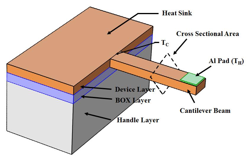
42 Chapter 2 Cantilever Beam Structure and Device Fabrication 2.1: Cantilever Beam Structure: Cantilever structure is a special type of device structure where one end of the beam is anchored with the substrate and the other side is free of having any contact. Intentionally making the length of the beam greater than the width and thickness heat transport can be manipulated as 1D system and analyze the thermal properties of the material. Design consideration were, a. Length > 4X Width b. Length >> thickness c. Infinite heat sink at the fixed end of cantilever beam d. Thin film transducer film at the free end for isotropic heat distribution A metal film of 80nm thickness were deposited at the free end of the cantilever beam for uniform heat absorption at the pump wavelength and good reflection at the probe wavelength. Aluminum was proffered as the metal transducer layer due to their good stiction with Si and relatively simple lift-off process for the fabrication. 2.2: Device Fabrication: i. Cantilever Beam: For the cantilever beam fabrication, Silicon on Insulator wafer was selected with a resistivity of the device layer of 1-20 ohm-cm, thickness of 1.291µm, box layer thickness of 1µm. Fabrication of the cantilever beam in SOI wafers is composed of following steps, 27
. The resistivity of the device layer for the wafers used was 0.01-0.02 Ohm-cm.")
 on the handle layer prevents higher residual stress in the")
43 1. The fabrication is performed on a SOI (Silicon on Insulator) wafer with device layer of m of Si, Buried Oxide or BOX of 1-2 m and handle layer of ~500 m thick Si. Crystal orientation on both the device layer and handle layer were (100). The resistivity of the device layer for the wafers used was Ohm-cm. The resistivity of the handle layer for the wafers used was 10 Ohm-cm. The lower resistivity on the device layer provides good electrical path on a MEMS device surface and a higher resistivity (less dopant) on the handle layer prevents higher residual stress in the wafer from buckling the freestanding beams upon release 2. Photomask was designed using AutoCAD and the designed Cantilever beam is patterned using AZ1518 photoresist, soft baked, exposed and developed tuning the photoresist profile. Figure 2.1: Photoresist pattern of cantilever beam 3. Then the Si is etched down to the BOX layer by Reactive Ion Etching process (RIE). With RIE, the plasma is generated by the application of a RF power source across two electrodes separated in a reactive, gaseous chemical mixture of electrons, ions, and free radicals which produce the distinct plasma glow. Initially, the plasma 28


44 consists of an equal number of positive and negative charges. Depletion of the charges in the plasma due to diffusion results in a layer of surface charge at the boundary of the plasma. Positive ions are accelerated within the chamber environment and aid in the etching process. The ion bombardment energy is controlled by the plasma potential. The wafer substrate on the lower electrode is exposed to the reactive neutrals and charge species. These species combine with the substrate material and create volatile products that etch the wafer. Since electrons are more mobile that ions, a DC self-bias voltage develops across the electrodes during the etch process to achieve the necessary current continuity. The self-bias voltage accelerates ions towards the wafer surface where they are react, cause various compounds to be desorbed, aid in the formation of polymers and help to facilitate the anisotropic etching. Etching can be attributed to two distinct mechanisms: chemical etching cause by free radicals and physical etching cause by ion bombardment. This process creates a high aspect ratio structure by etching vertically down from the edge of the PR layer. Figure 2.2: Microscopic image after RIE etch 29


45 Next, the PR layer is removed using acetone, isopropyl alcohol, and de-ionized water rinses respectively 4. The wafers are then released using Buffered Oxide etch in a 20:1 diluted HF to get the uniform etching all over the area. When the cantilever beam were fully released the wafers are rinsed with DI water and dried for the next step. 5. Next the wafer is coated again with the PR sufficiently thick to cover the entire high aspect ratio structure. The PR is then patterned for the deposition of Aluminum at the free end of the cantilever beam. Aluminum deposition was performed in ultrahigh vacuum (<10-6 Torr) using a e-beam source with a constant deposition rate of 2A /s. 80nm thickness of the Aluminum layer was confirmed with profilometer. Then the wafers were submerged in a acetone remove the access Aluminum from the other area by removing the PR and this process is commonly known as lift-off process. Then the wafers ere rinsed with IPA and water and dried. Figure 2.3: Microscopic Al pad deposition and lift off 6. After the samples were released, they were immersed into Critical Point Dryer for a full cycle with IPA to avoid any stiction failure of the devices. 30

46 7. As soon as the sample were prepared it was diced into small pieces and the substrate from the back of the cantilever beam were cleaved precisely to be able install in the vacuum chamber and for both directional probing along the beam. (a) 31

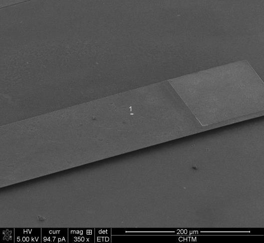

47 (b) (c) 32

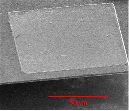
48 (d) Figure 2.4: (a) Fabrication Steps; (b) Device Structure; (c) SEM images; (d) cleaved sample ii. Semi-infinite Sample: Second set of samples were fabricated depositing Aluminum film on bare Si wafer maintaining all the evaporation parameters of the cantilever beam s Al pad. The bare Si wafer s specification of resistivity, orientation kept similar to the device layer of the SOI wafers that were used to fabricate the cantilever beams. These planar structure sample is been used to measure the thermoreflectance coefficient of the Aluminum film (80nm) which needed to be applied on the measurement of the cantilever beam thermal properties. 33
49 Chapter 3 Steady State Analysis Steady state conduction is the form of conduction that happens when the temperature difference(s) driving the conduction are constant, so that (after an equilibration time), the spatial distribution of temperatures in the conducting object does not change any further. Thus, all partial derivatives of temperature with respect to space may either be zero or have nonzero values, but all derivatives of temperature at any point with respect to time are uniformly zero. In steady state conduction, the amount of heat entering any region of an object is equal to amount of heat coming out. Fourier s law can be applied in the steady state condition as there is only one free parameter,thermal conductivity need to be measured and it does not have any heat capacity involved with the equation. For a linear material in a cantilever beam if one end of the beam is pumped with heat, the temperature drop across the beam will be linear and it will constantly reduce with the ration of thermal conductivity. The relationship of Fourier s law to the heat conduction equation has been described at the section Theory: For the steady state case all assumption are applied for analysis and those are Heat transfer mechanism is only due to conduction 1 directional flow of heat transfer, Bounding surfaces are isothermal in character that is constant and uniform temperatures are maintained at the two faces Isotropic and homogeneous material and thermal conductivity k is constant 34
50 Constant temperature gradient and linear temperature profile Measurement of Thermoreflectance Coefficient of Aluminum for Semi-infinite Structure: Thermoreflectance coefficient of Aluminum film varies due to its deposition technique, source material being deposited, deposition pressure etc. For this it is very essential that the thermoreflectance coefficient of Aluminum is been measured and calibrated for the experiments, otherwise erroneous result lead into erroneous measurement of the thermal properties in all steps. 80 nm of aluminum was deposited on the topside of the cantilever beam structures at the free end to enhance the absorption of the pump laser. The thermoreflectance coefficient, CTR, of aluminum films vary due to deposition parameters, source material being deposited, deposition pressure etc. 38,39,42 Therefore it is essential to accurately measure the thermoreflectance coefficient of Al for the exact film deposited in a given set of experiments.. 6,7 T = P abs 2 πr spot κ bulk (3.1) Where, Pabs is the absorbed power calculated from the incident and reflected power, rspot is the pump and probe beam radius incident on the sample and κbulk is the thermal conductivity of bulk Silicon. Change of reflectivity from the sample is directly proportional to the change of temperature and can be expressed by the eqn ,37,43 46 R R = (1 R R T ) T = C TR T (3.2) where, R is the reflectivity from the cantilever beam is not heated and ΔR is the change of reflectivity due to heating, CTR is the thermoreflectance coefficient of Al. 35
51 3.1.2 Steady State Analysis for Cantilever Beam: A pump probe technique with steady heat flux generated by a Continuous Wave Laser is used for the measurement of thermal conductivity of free-standing thin Si film. For Steady state 1D heat flux, q " = κ T x (3.3) Where q is heat flux, T is the temperature and k is thermal conductivity of the thin film. Which gives the solution for thermal conductivity for temperature difference of T and the beam length is L, 47 κ = q" T (L x) (3.4) In this experiment, thermoreflectance response were measured along the beam length (backside technique) and the thermoreflectance response is extracted for the position of tip with Al pad. Using the front side technique ΔT is measured at the tip and Ctr of Si is extracted from the backside ΔR/R values at tip with eqn The temperature profile along the beam length is obtained using the Silicon s thermoreflectance Coefficient and ΔR/R with eqn This temperature distribution and absorbed heat flux used with eq. 3.4 to get the thermal conductivity of Si. 3.2 Experimental Setup: The experimental analysis has been established using two CW laser one as the heating pump beam at the wavelength of 670nm and the other one is for the probing at the 36
52 wavelength of 532nm. In this study the pump beam power has been varied for different analysis but the probe beam power kept constant and which is very small( <1% of the pump power) comparing the pump beam power and does not have any effect on the rise of temperature. The pump and probe laser connected to laser diode controller and temperature controller. The temperature of the laser diodes were kept in the range of 20 C to 25 C. Laser diode temperature in the operating range is very important as the Laser power oscillates at higher temperature. The pump and probe beam passes thru to separate wavelength isolator to prevent reflection reaches laser which can impact on the laser lifetime and can cause undesired heating of the laser from the reflected beam. A regular experimental setup for the steady state measurement is shown in figure 4 for a demonstration purpose but the setup has been used in a different arrangement for the backside temperature profile measuring which has been described later. 37
53 Figure 3.1: Basic Steady State Thermoreflectance Measurement Setup The samples were placed in a vacuum chamber with a turbo molecular pump and roughing pump for a high vacuum up to 1X10⁻⁷ Torr to prevent convective loss and the radiation loss was also minimized by cleaving the substrate from the cantilever beam Spot Size Measurement: Spot size of the pump and probe beam were measured using a CCD camera showed in fig. 3.2 and the image thru a thin film membrane of the spot size radius were calibrated for different focal length of the lens and the smallest pump and probe beam was measured to the 1/e 2 value of 5.92 µm. 38
54 Figure 3.2: Spot size imaging setup For the measurement of the laser spot size thin film membrane with substrate etched from the backside of the wafer was used. Thin film membrane had metal strip lines of 30µm width as a reference to measure the actual size of the spot size reflecting from the surface of the film. The focal length of the length before the sample to be incident has been calibrated for different spot sizes. An image from the CCD camera of the spot size (a) and calibrated spot size with reference to the metal strip lines (b) are shown in fig


55 Figure 3.3: Spot Size Imaging Setup; (b) Spot size image Vacuum Chamber Fabrication: Two types of vacuum chamber were fabricated for the cantilever beam thermoreflectance measurement which are shown in fig The vacuum chamber shown in fig. 3.4 is comparatively small with both glass view port with the capability of installing free standing cantilever beam in a stage. The chamber is capable of being attached to optical stage easily for x,y,z direction calibration during measurement. The design of the chamber from the one side of glass to the other side of the glass were maintained with the focal length of the lens from the both side. The chamber is capable of holding pressure in the 10-7 Torr with very low leak rate. The chamber was connected to the pump using flexible vacuum line to avoid any kind of vibration and gate valve has been used to isolate the chamber portion from the pump during the measurement. The other type of vacuum chamber is shown chapter 6 which is primarily designed for low temperature application. The chamber has two different compartment inside and outside 40
 and the inside compartment can be filled with liquid Helium for lower temperature (upto 3mK) application.")
 and chamber with a handle to be attached to the optical stage is shown in (b)")
56 chamber to be filled with liquid nitrogen and the sample compartment is installed with two view port capable of pumping down to 10-7 Torr. The chamber was tested for liquid Nitrogen temperature (77K) and the inside compartment can be filled with liquid Helium for lower temperature (upto 3mK) application. Comsol simulation has been done on the entire design to make sure the whole system work up to liquid nitrogen temperature and shown in chapter 6. (a) (b) Figure 3.4: High Pressure small vacuum chamber for thermoreflectance measurement; the cross section of the chamber is shown in (a) and chamber with a handle to be attached to the optical stage is shown in (b) Topside probing: Fig. 3.6 shows the experimental setup for pump-probe thermoreflectance measurements for topside probing of semi-infinite substrates and the topside of the cantilever beams. Aluminum was deposited on the tip of the cantilevers due to its 41
57 compatibility with Si and for its absorption at the pump wavelength. A 670 nm pump laser (CW) first travels through an optical isolator which prevents back-reflection. The 532 nm probe laser (CW) passes through its own optical isolator before the beam sampler. The beam sampler is aligned such that it co-aligns the beams then passes through a beam splitter and allows the pump and probe beams to continue travelling towards the sample. An objective lens was used to focus the pump beam s diameter to 20µm (for semi-infinite measurements) and to the width of the Al pad for the measurement of the cantilever beam structure. The probe beam was always kept to a spot size of 6µm (1/e value) for all experiments. The reflected probe beam is passed thru a laser line filter and travels toward a photodiode. Depending on the change of the temperature induced by the pump beam, the reflectivity of the sample changes and it is detected at the photodiode. 6,7,41 The reference photodiode is used to measure the incident pump beam s power. However the reflected pump beam s power can be measured using a 670 nm laser line filter placed in front of the photodiode instead of a 532 nm laser line filter. By measuring the incident and reflected beam powers the absorbed power can be determined by using A = I-R, where I is incident pump power and R is the reflected pump power. Note that there is no transmission. 42

58 Figure 3.5: Top side measurement beam incident on cantilever beam The topside thermoreflectance technique is also utilized to measure the thermoreflectance coefficient of the Al films deposited on the semi-infinite Si wafer to use as the coefficient of thermoreflectance. Figure 3.6: Transducer side thermoreflectance measurement setup for Semi-infinite and cantilever beam at tip The front side thermoreflectance technique is used to measure the 43

59 thermoreflectance coefficient of Al film deposited on the semi-infinite Si wafer and the change of reflectivity from Al pad tip of the cantilever beam Thermal Gradient Probing: In figure 3.8 experimental setup for thermoreflectance measurement is shown labeling all the components. In this experiment the probe beam incident on the cantilever beam s backside to measure the reflectivity along the beam length for calculating the thermal conductivity of the structure. 6,7,48 The substrate were cleaved for the free suspension of the cantilever beam. Figure 3.7: Thermal gradient measurement architecture along the cantilever beam. 44
60 Figure 3.8: Thermal gradient measurement setup for thermoreflectance along the cantilever beam. The change of thermoreflectance needs to be correlated with the photodiode measured voltage The measured voltage by a photodiode is a representation of photocurrent which is converted to voltage and correlated with the responsivity of photodiode and which is directly proportional to the reflectance from the sample. The measurement also needs to be calibrated for the responsivity of the photodiode at that particular frequency. The measured output voltage of a photodiode is related with the transimpedance gain and the responsivity of the photodiode. The photodiode responsivity for a particular wavelength can be found from the product data sheet. Out Put ( V W ) = Transimp. Gain (V A ) Responsivity (A W ) (3.5) 45
61 3.3 Results: Experimental measurement for steady state analysis has been demonstrated in this section by step by step analysis. It starts with calibrating the Aluminum thermoreflectance coefficient on a semi-infinite sample and measure it for range of incident laser power. Then apply the value of Al thermoreflectance coefficient for cantilever beam to get the reference temperature point at the free end of cantilever. Then it continuous by measuring thermoreflectance coefficient of Si by measuring the change of reflectance along the beam and use that to extract the temperature gradient and the find thermal conductivity for Si. All the measurements are demonstrated in this section with necessary description Thermorfeflectance Coefficient of Aluminum Measurement: The semi-infinite Al on bulk Si sample were used to measure the thermoreflectance coefficient of Al to be able to use it for further analysis on cantilever beam structure. Using the technique described at section and the experimental setup of transducer side setup to measure the thermoreflectance coefficient of Al where the pump spot size was kept to 20.5µm and the thermal conductivity of bulk Si were used W/m-K 28 which was confirmed using a TDTR technique. The thermoreflectance plot of planar Al on Si is shown in fig. 3.9 and the thermoreflectance Coefficient of Al is measured to be K 1. 38,39,42 46
62 Figure 3.9: Aluminum Thermoreflectance Coefficient for different incident power level Cantilever beam tip temperature measurement: With the help of eqn. 3.2 and the transducer side setup described at section with the knowledge of the thermoreflection coefficient of Aluminum of K 1, the temperature of the free end of the cantilever beam can be known my measuring the change of reflectance for different incident pump power. In this experiment the incident pump power, reflected pump power were also measured using photodiode and transmitted power is negligible thru the Al transducer layer comparing to the incident or reflected pump power Change of reflectance along the beam measurement: Thermoreflectance response of a Cantilever beam of 100µm width and 400µm long for different input flux at high vacuum (1X10⁻⁷ Torr) shown in fig In this pressure, heat 47
63 is only transported due to conduction and this experiment was conducted on different length beam keeping the width fixed and changing the width as well, in all cases the thickness of the cantilever beam were constant to be 1.29µm. In this experiment the change of reflectance were measured at least 50µm away from the end of the Al pad which was 90μm 90μm at the free end of the cantilever beam to avoid any kind of effect non parallel isotherm along the width close to the pump spot. Figure 3.10: Change of reflectance along the beam length of a cantilever beam from the free end to the anchored side. Different power level of incident pump beam is shown to illustrate how the profile is changing Measurement of Thermoreflectance Coefficient of Si: By extracting linear fit value of the R R to the position of the pump spot at the Al pad, with the knowledge of temperature at that point described at section and using eqn. 3.2 the 48
64 thermoreflectance coefficient of Si can be measured and the measured value of thermoreflectance coefficient (C TR_Si ) of Si is K Thermal Gradient profile extraction along the beam: The temperature profile of the cantilever beam along the beam length can be extracted by knowing the thermoreflectance coefficient of Si, change of reflectance R R from section and using the thermoreflectance eqn Which is the essential part of the thermal conductivity measurement in steady state condition using Fourier s law. The temperature gradient profile along the cantilever beam is shown in fig Figure 3.11: Temperature profile along the beam length extracted from the thermoreflectance measurement. 49
65 3.4.6 Thermal Conductivity of Si cantilever Beam: Using temperature gradient in Fourier s law (eqn. 3.3) obtained from the previous part the thermal conductivity can be measured for the cantilever beam. The unknown term in this equation is the flux of pump laser. The absorbed power was measured by measuring the incident, reflected and the transmitted power using photodiode. The transmitted power was negligible comparing to the incident or the reflected power. Measuring the absorbed power for all the beam separately and the measuring all the temperature gradient for beam width of 100µm and 150µm and length of 400µm, 500µm and 750µm, 1050µm respectively the thermal conductivity was measured to be 96.9 ± 1.76 Wm 1 K 1.The thermal conductivity value for 10 different measurement is shown in fig Figure 3.12: Thermal Conductivity of at different power levels of the incident pump beam. 50
 and the result for nanowire like structure is shown in figure 3.13(b). Figure 3.")
66 3.5 Constraint Validation: D Heat Transfer Validation: FEM simulations were conducted to establish the constant isotherm for differential heat flow in the beam length direction. Simulation result for the single beam of 50µm width is shown in figure 3.13(a) and the result for nanowire like structure is shown in figure 3.13(b). Figure 3.13: Heat flux FEM simulation results for slab structure; (b) heat flux FEM simulation results for isotherm analysis of cantilever beam. 51
67 In this study, Isotherm becomes constant or negligible amount of change below 5% of the temperature change from the center to the edge with in the 5% of the length of the beam starting from the edge of the Aluminum pad. Constant isotherm of 95% of the beam length proves the 1D heat flow along the beam length. There were other different studies were performed to see how the isotherm effects along the beam length if the pump beam spot is not centered or even smaller. In these cases isotherm starts to deviate more than the placed at center of the pad and covered the whole Al pad. In our experiment, we always maintain the pump spot cover the whole pad to avoid these issues Temperature Boundary condition Validation The cantilever beams reflectivity from the tip were analyzed to characterize the boundary condition limitation. Thermoreflectance from the tip is linear at moderate incident pump power shown as common input power operating zone in the figure and reflectivity changes linearly. As the input power goes high we observe transition period of the reflectivity and beyond that the reflectivity increases. The transition period occurs at different input power for different cantilever beam length which is a sign of elevation of the base temperature from the room temperature of heat sink. 52
68 Figure 3.14: Thermoreflectance from cantilever beam tip for varying power, higher incident power induces non continuity of the linear response of thermoreflectance. To maintain the boundary condition the experiments needed to conduct in the incident laser power regime showed in fig with circled region. Incidence of higher laser power can cause damage to the Al pad which can change the thermoreflectance property of Al as Aluminum is a low melting point metal and erroneous result can baffle the experiment. The incident laser power has a lower limit too where the emitting laser power is not linear with the applied current in this portion of the laser operation laser power can fluctuate over time ending up in less consistency. 3.6 Validation of only Conduction Convective Loss: Convective heat loss along the beam length is an important factor in the steady state condition of the thermoreflectance analysis. As our experiment is not conducted using a 53
69 ultra-short heat pulse, the convective loss can play an important role measuring thermal properties of the cantilever beam. The samples were placed in a vacuum chamber with a turbo molecular pump and roughing pump for a high vacuum up to 1X10⁻⁷ Torr to prevent convective loss. The experiments were conducted in different pressure from the atmospheric pressure to 1X10⁻⁷ Torr. The pump beam was incident on a part of Silicon and the probe beam was 100µm distant from the beam and the change of reflectivity with pressure is measured. As the pressure goes down below 10-4 Torr, the change of reflectivity saturates in higher value and the measurement in this range will have less error in results for conductive heat transfer. For the atmospheric and low vacuum condition heat loss was observed from the thermoreflectance data with different pressure is shown in fig The heat loss due to convection can be avoided in high vacuum condition observed from the thermoreflectance data. Figure 3.15: Thermoreflectance response of a constact pump and probe beam displacement for a 2.4 mm cantilever beam from atmospheric pressure to 1X10⁻⁷ Torr. 54
70 3.6.2 Radiative Loss: The radiation loss was minimized first of all by releasing the devices from the substrate and later the substrate from the underneath of the cantilever beam were cleaved and minimizing any kind of radiative loss from the measurement. The input power were also maintained in lower regime to prevent radiative loss. 55
71 Chapter 4 Harmonic Analysis 4.1 Theory: Semi Infinite Frequency Domain Thermoreflectance Analysis: Harmonic analysis needs to be performed using a lock-in amplifier which measures the fundamental harmonic component of the probe signal at the modulation frequency and rejects all other components. The output of the lock in amplifier consists of amplitude A and phase (φ) with respect to the reference wave of the fundamental component of the probe signal with respect to the reference wave. Mathematically, the solution can be expressed as, 11,12,41,48 Ae i(ω0t+φ) = Z(ω 0 )e iω 0t (4.1) In case of cw laser the solution is in the form, Z(ω 0 ) = βh(ω 0 ) (4.2) In the frequency domain, temperature (θ) and heat flux (f) of the top and bottom side can be related as, [ θ b cosh (qd) ] = [ f b σ z q sinh (qd) 1 sinh (qd) σ z q ] [ θ t ] (4.3) f t cosh (qd) Here d is the layer thickness, σz the cross-plane thermal conductivity and q 2 = σ rk 2 + ρciω σ z (4.4) where ρ is the density, c is the specific heat capacity, and σr is the radia thermal conductivity and and σz is the cross-plane thermal conductivity. Hankel transform of a Gaussian spot 56
72 with power A0 and 1/e 2 radius w0, The heat flux boundary condition at the top layer ft is given by, f t = A 0 2π exp w 2 ( k2 0 ) (4.5) 8 Multiplying the matrices for individual layers together [ θ b ] = M f n M n 1. M 1 = [ A b C B D ] [θ t ] (4.6) f t where Mn is the matrix for the bottom layer. In the limit of the heat capacity of a layer approaches zero (G=z /d ) and the bottom surface of the nth layer is adiabatic or semiinfinite, then in both cases eqn. 4.6 reduces to C t + Df t = 0 and the surface temperature will be in the form of, 9,41 θ t = D C f t (4.7) The final frequency response H (ω) in real space is found by taking the inverse Hankel transform of eqn. 4.7, H(ω) = A 0 2π 0 k( D )exp[ k2 (w w 2 1 ]dk C 8 (4.8) Solving eqn. 4.8 analytically and using eqn. 4.1 and 4.2 the phase response in the frequency domain can be achieved D Harmonic Thermoreflectance for Free Standing Structure: The phase-shift method has been widely used to measure the thermal diffusivity of thinfilm materials. A sinusoidal heat flux is generated by applying a modulated pump laser beam at the pad of the cantilever beam in fig The 1D transient heat conduction can be formulated as, 57
73 with an initial condition and boundary conditions, T t = α 2 T (4.9) x 2 T(x, 0) = T 0 T(L. t) = T 0 k T x = T 1 Sinωt x=0 Using Complex Temperature Method the solution of eqn. 8 will be, T(x, t) = T 0 + T 1 sin (ωt x ω 2α )e x ω 2α (4.10) Phase difference along the beam, = ω 2α x Using finite element method for the solution of the eqn The analytical and numerical solution are shown in fig
74 Figure 4.1: Analytical and Numerical analysis result of cantilever beam in harmonic case from the frequency ranging from 10 Hz to 100Hz 4.2 Experimental Setup: In fig. 4.4 experimental setup for thermoreflectance measurement is shown labeling all the components. In this experiment the probe beam is modulated by an electro-optic modulator after it passes through the isolator. The signal generator is to generate sinusoidal signal and the Lock in Amplifier measures the amplitude and the phase of the signals. 6,7,48 The experimental setup was designed in such a way that the input pump beam travel towards the Al tip from the front side passing through isolator, EOM, beamplitter and probe beam comes from the back of the cantilever beam and when it reflects back due to the temperature oscillation the reflected beam end up being modulated and detected in the photodiode. With 59
75 reference to the input pump beam the phase change of the probe beam can be measured using Lock in Amplifier. Figure 4.2: Modulated Incident pump beam and thermally modulated reflected probe beam for harmonic analysis Lock in Amplifier is an essential equipment in harmonic analysis due to its capability of detecting signal buried under the noise. As our measurement is in the range of nano volts, it is necessary to extract the change of voltage signal rejecting all the noise contributing due to electronic noise, vibration, laser oscillation etc. Precautionary measure were taken to eliminate all the noise source can affect the measurement. Lock-in amplifier measures signal at a reference frequency feed as input from the signal generator which is the frequency of the laser that is oscillating as an input to the cantilever beam. The lock in Amplifier only can detect signal at this frequency other frequency oscillation are eliminated 60
76 by Phase Locked Loop circuitry. In the following diagram, the reference signal is a square wave at frequency ω r. This might be the sync output from a function generator. If the sine output from the function generator is used to excite the experiment, the response might be the signal waveform shown below. The signal is V sig sin(ω r t + θ sig ) where V sig the signal amplitude is, ω r is the signal frequency, and θ sig is the signal s phase. Lock-in amplifiers generate their own internal reference signal usually by a phase-locked-loop locked to the external reference. In the diagram, the external reference, the lock-in s reference, and the signal are all shown. The internal reference is V L sin(ω L t + θ ref ) Figure 4.3: Lock in Amplifier operation with respect to reference signal to measure the real signal s phase shift 49 The lock-in amplifies the signal and then multiplies it by the lock-in reference using a phase-sensitive detector or multiplier. The output of the PSD is simply the product of two Sine waves. 61
77 V psd = V sig V L sin(ω r t + θ sig ) sin(ω L t + θ ref ) = 1 2 V sigv L cos([ω r ω L ]t + θ sig θ ref ) 1 2 V sigv L cos([ω r + ω L )t + θ sig + θ ref ) If the PSD output is passed through a low pass filter, the AC signals are removed. And in this case, the filtered PSD output will be: V psd = 1 2 V sigv L cos(θ sig θ ref ) If second PSD multiplies the signal with the reference oscillator shifted by 90, i.e. V L sin(ω L t + θ ref + 90 o ), its low pass filtered output will be: V psd2 = 1 2 V sigv L sin(θ sig θ ref ) V psd2 ~ V sig sin θ Now we have two outputs: one proportional to cos θ and the other proportional tosin θ. If we call the first output X and the second Y, X = V sig cos θ; Y = V sig sin θ these two quantities represent the signal as a vector relative to the lock-in reference oscillator. X is called the 'in-phase' component and Y the 'out of phase' component. This is because when θ = 0, X measures the signal while Y is zero. By computing the magnitude (R) of the signal vector, the phase dependency is removed. R = X 2 + Y 2 = V sig R measures the signal amplitude and does not depend upon the phase between the signal and lock-in reference. A dual-phase lock-in has two PSDs with reference oscillators 90 apart, and can measure X, Y and R directly. In addition, the phase (θ) between the signal and lock-in is defined as: 49,50 62
78 θ = tan 1 ( Y X ) Characterize the thermoreflectance behavior for micro and nano scale cantilever beam structures. The width of the beams are 50µm, 100µm, 150µm, 200µm, 250µm, 300µm and the minimum length is of the beams are four times of the corresponding width length. The resistivity of the of the device layer were kept in the range of 1-20 Ω-cm with 100 crystal orientation and the box layer thickness were in between 1-2µm. Figure 4.3: Harmonic analysis setup for topside thermoreflectance measurement 63
79 Figure 4.4: Setup for harmonic analysis setup for backside thermoreflectance 4.3 Results: The experimental analysis of harmonic analysis were performed first of all validating the setup with Malen et. al. 6 with their measurement of semi-infinite bulk measurement and then Aluminum of 80nm film were deposited on top of bulk to Si to validate the result 64
80 using TDTR technique. After validating both of the results, experiment on cantilever beam were conducted and those are described below in different section : Semi Infinite Sample Result validation: Harmonic thermoreflectance setup for semi-infinite sample shown in fig The experimental data is in good agreement with the theory for the fitting parameter of thermal conductivity with the value of 117 W/m-K shown in fig The phase response for the bulk Si was validated with malen et al shown in fig Figure 4.5: Semi-infinite sample result validation with malen et at. 6 65
81 Figure 4.6: Semi-infinite result fit with the analytical analysis Cantilever Beam Phase Response: Phase response of a cantilever beam was measured along the length of the cantilever beam and the phase difference between two pints 400µm and 600µm are well fitted with the analytical result shown in fig In the frequency range of Hz the heat capacity 764 Jkg 1 K 1 has been measured. Higher frequency oscillation has effect of resonance and the time constant of the structure which prevents high frequency operation of the beam. 66
82 Figure 4.7: Cantilever beam phase response between 400µm and 600µm from the center of the Aluminum pad of the free end of the cantilever beam. 67
83 Chapter 5 Transient Analysis 5.1 Theory In cartesian coordinate, the heat equation can be expressed as below, T t = α 2 T (5.1) x 2 where, α is the thermal thermal diffusivity and expressed in terms of thermal conductivity ҡ, heat capacity C and density ρ as C. with an initial condition and boundary conditions, T(x, 0) = T 0 The solution can be derived in the form of, T(L. t) = T 0 k T x = { T 1, 0 < t < t 0 x=0 0, t > t 0 T(0, t) = T 0 + T 1 (1 exp t τ) (5.2) Where, the time constant for the temperature rise and decay for 1D structure can be approximated as, τ = L2 here L is denoted as the cantilever beam length and heat capacity α can be extracted by inserting the value of thermal conductivity measured from the steady state technique. For the transient analysis of cantilever beam numerical analysis were performed and the result of numerical analysis follows closely to the analytical value obtained from the experiment below. 68
84 5.2 Experimental Setup: The experimental setup was kept similar as of the harmonic analysis shown in figure 5.1, in this case low frequency pulse function was generated using the function generator passing thru the EOM to modulate the pump beam, and the probe beam was used from the bottomside of the sample to measure the transient change in the thermoreflectance. All the measurement were performed at the pressure Torr where convection does not have any impact on the result. Figure 5.1: Setup for harmonic analysis setup for backside thermoreflectance 69
85 5.3 Results: Pulse input of a transient pump beam incident on cantilever beam and the change of reflectivity due to temperature rise is analyzed and measured time constant were fitted for the extraction of specific heat capacity using the thermal conductivity measured in the steady state analysis. In this experiment the EOM modulation with other optical component such as wave plate, linear polarizer were monitored very carefully to make sure the pulse reaches its peak value or decay its lowest value without effecting the rise or fall time. Longer pulse duty cycle were chosen to make the saturated value is long enough and does not impact the time constant. On the other hand, it is very import to look after if the photodiode is getting saturated or not. The pump or probe power kept small enough or using Neutral Density filter to cut off the power before reaching to the photodiode and does not saturate. Saturated photodiode can produce erroneous measurement data hence erroneous time constant. For this region lower frequency pulse cycle were chose due to fact that cantilever beam reaches to its resonance frequency in higher frequency range which does not provide any result for the transient analysis. The pump and probe beam transient analysis result shown in figure
86 Figure 5.2: Transient temperature response using pump probe technique on cantilever beam Several measurements were performed in this analysis with different input power and the rise time and the fall time were measured for the cantilever beam. The rise and fall time were very in close proximity and their results are shown in figure 5.3. Figure 5.3: Analysis of rise and fall time with different incident laser power The average value of rise and fall time of 35.5ms for 1.4mm long cantilever beam was measured and the thermal conductivity measured using steady state technique of 96.9 Wm 1 K 1 has been used to measure the heat capacity at, τ = L2 ; the heat capacity of Si has measured to be 753 JKg 1 K 1. Which is very close to the value that we have measured using harmonic analysis. α 71
87 Chapter 6 Conclusion and Future Work The pump-probe thermoreflectance technique was demonstrated in steady state, harmonic and transient conditions for thermoreflectance coefficient, thermal conductivity, specific heat capacity measurement of free standing Si cantilever beams. Measurements were conducted in high vacuum to avoid convective losses and with no substrate to minimize radiative losses. Temperature gradients were minimized such that linear thermoreflectance response can be related to the measurements of thermal conductivity. Four cantilever beams 1.29 µm thick were measured and determined to have an average thermal conductivity of 96.9 ± 1.76 Wm -1 K -1, which is a ~30% reduction from bulk values and applying harmonic and transient analysis of 1D free standing beam specific capacity also deduced with a value of 760 JKg 1 K 1 which does not have much changes from its bulk. So far we have able to establish a way to measure thermal conductivity at steady state condition for cantilever beam, harmonic and transient analysis to extract heat capacity using the thermal conductivity achieved from the steady state condition. For the establishment of the work, all the parameters of the experiment spot size, 1D heat conduction validation using FEM, convection effect on the thermoreflectance, radiation, boundary condition were analyzed step by step and demonstrated throughout the manuscript. Several measurement analysis can be extended using this study for future research. 72
88 1. Analysis of thermal Conductivity with Various Film Thickness: The main goal would be to apply these three technique for different thickness of Si cantilever beams and extrapolate the variation of thermal conductivity and heat capacity with the film thickness and demonstrate size effect variation from the bulk. 3,43,51 Figure 6.1: Thermal conductivity variation with film thickness extracted from different author and comparison to our analysis 2. Measurement at Cryogenic: The setup for the cryogenic measurement is shown in figure 6.2 and 6.3. The cryo set up needs to be designed in such a way that the sample can be easily placed in the chamber without having any interference from the liquid nitrogen or helium pouring in to the chamber. The chamber also needed to be designed in such a way that the chamber have optical view port from both of the direction to allow laser beam to be accessible in the chamber to the cantilever beam. Using this technique the variation of thermal properties of different films at low temperature can be demonstrated and the identify size effect of microscale scale structure in the variation of thermal properties from the bulk and which is 73


89 necessary to measure accurately for low temperature device application or for thermoelectric materials. Figure 6.2: Cryogenic setup design for low temperature application 74


90 Figure 6.3: installation of Cryogenic Setup for low temperature measurement application 3. Phononic Crystal Structure Measurement: The analysis of different thickness of Si cantilever beam will give a better insight of the variation of thermal conductivity and heat capacity. And applying it to phononic crystal structure provide better insight of thermal property variation due to the change phonon mean free path. Phononic device structure is constructed in such a way that air holes are fabricated intentionally in a materials where the dimensions are smaller than the mean free path of phonon which introduces more scattering in heat conduction and effect the material property which are useful for low temperature application and also to manipulate for wideband gap phononic structure devices. 75

91 Figure 6.4: Phononic Crystals along the slab of cantilever beam to compare thermal conductivity variation with their slab counterpart. 76
Institute for Electron Microscopy and Nanoanalysis Graz Centre for Electron Microscopy
 Institute for Electron Microscopy and Nanoanalysis Graz Centre for Electron Microscopy Micromechanics Ass.Prof. Priv.-Doz. DI Dr. Harald Plank a,b a Institute of Electron Microscopy and Nanoanalysis, Graz
Resistance Thermometry based Picowatt-Resolution Heat-Flow Calorimeter
 Resistance Thermometry based Picowatt-Resolution Heat-Flow Calorimeter S. Sadat 1, E. Meyhofer 1 and P. Reddy 1, 1 Department of Mechanical Engineering, University of Michigan, Ann Arbor, 48109 Department
Supplementary Figures
 Supplementary Figures Supplementary Figure S1. The effect of window size. The phonon MFP spectrum of intrinsic c-si (T=300 K) is shown for 7-point, 13-point, and 19-point windows. Increasing the window
Chapter 5. Effects of Photonic Crystal Band Gap on Rotation and Deformation of Hollow Te Rods in Triangular Lattice
 Chapter 5 Effects of Photonic Crystal Band Gap on Rotation and Deformation of Hollow Te Rods in Triangular Lattice In chapter 3 and 4, we have demonstrated that the deformed rods, rotational rods and perturbation
On the Steady-State Temperature Rise During Laser Heating of Multilayer Thin Films in Optical Pump Probe Techniques
 Jeffrey L. Braun Department of Mechanical and Aerospace Engineering, Charlottesville, VA 22904 Chester J. Szwejkowski Department of Mechanical and Aerospace Engineering, Charlottesville, VA 22904 Ashutosh
MEMS Tuning-Fork Gyroscope Mid-Term Report Amanda Bristow Travis Barton Stephen Nary
 MEMS Tuning-Fork Gyroscope Mid-Term Report Amanda Bristow Travis Barton Stephen Nary Abstract MEMS based gyroscopes have gained in popularity for use as rotation rate sensors in commercial products like
Homework Week 3: Nanoscale and macroscale characterization Thermoelectricity: From Atoms to Systems
 Homework Week 3: Nanoscale and macroscale characterization Thermoelectricity: From Atoms to Systems Je-Hyeong Bahk and Ali Shakouri nanohub-u Fall 2013 Answer the thirteen questions including all the sub-questions
Phonon and Electron Transport through Ge 2 Sb 2 Te 5 Films and Interfaces Bounded by Metals
 Supporting Online Material for Phonon and Electron Transport through Ge 2 Sb 2 Te 5 Films and Interfaces Bounded by Metals Jaeho Lee 1, Elah Bozorg-Grayeli 1, SangBum Kim 2, Mehdi Asheghi 1, H.-S. Philip
Slide 1. Temperatures Light (Optoelectronics) Magnetic Fields Strain Pressure Displacement and Rotation Acceleration Electronic Sensors
 Magnetic Fields Strain Pressure Displacement and Rotation Acceleration Electronic Sensors") Slide 1 Electronic Sensors Electronic sensors can be designed to detect a variety of quantitative aspects of a given physical system. Such quantities include: Temperatures Light (Optoelectronics) Magnetic
Slide 1 Electronic Sensors Electronic sensors can be designed to detect a variety of quantitative aspects of a given physical system. Such quantities include: Temperatures Light (Optoelectronics) Magnetic
UNIT 3. By: Ajay Kumar Gautam Asst. Prof. Dev Bhoomi Institute of Technology & Engineering, Dehradun
 UNIT 3 By: Ajay Kumar Gautam Asst. Prof. Dev Bhoomi Institute of Technology & Engineering, Dehradun 1 Syllabus Lithography: photolithography and pattern transfer, Optical and non optical lithography, electron,
Thermal Sensors and Actuators
 Thermal Sensors and Actuators Part I Fundamentals of heat transfer Heat transfer occurs where there is a temperature gradient until an equilibrium is reached. Four major mechanism Thermal conduction Natural
DEPOSITION OF THIN TiO 2 FILMS BY DC MAGNETRON SPUTTERING METHOD
 Chapter 4 DEPOSITION OF THIN TiO 2 FILMS BY DC MAGNETRON SPUTTERING METHOD 4.1 INTRODUCTION Sputter deposition process is another old technique being used in modern semiconductor industries. Sputtering
SUPPLEMENTARY MATERIALS FOR PHONON TRANSMISSION COEFFICIENTS AT SOLID INTERFACES
 148 A p p e n d i x D SUPPLEMENTARY MATERIALS FOR PHONON TRANSMISSION COEFFICIENTS AT SOLID INTERFACES D.1 Overview The supplementary information contains additional information on our computational approach
EE C247B / ME C218 INTRODUCTION TO MEMS DESIGN SPRING 2014 C. Nguyen PROBLEM SET #4
 Issued: Wednesday, Mar. 5, 2014 PROBLEM SET #4 Due (at 9 a.m.): Tuesday Mar. 18, 2014, in the EE C247B HW box near 125 Cory. 1. Suppose you would like to fabricate the suspended cross beam structure below
Fadei Komarov Alexander Kamyshan
 Fadei Komarov Alexander Kamyshan Institute of Applied Physics Problems, Belarusian State University, Minsk, Belarus KomarovF@bsu.by Tasks and Objects 2 Introduction and motivation Experimental setup designed
Electronic thermal transport in nanoscale metal layers
 Electronic thermal transport in nanoscale metal layers David Cahill, Richard Wilson, Wei Wang, Joseph Feser Department of Materials Science and Engineering Materials Research Laboratory University of Illinois
Kavli Workshop for Journalists. June 13th, CNF Cleanroom Activities
 Kavli Workshop for Journalists June 13th, 2007 CNF Cleanroom Activities Seeing nm-sized Objects with an SEM Lab experience: Scanning Electron Microscopy Equipment: Zeiss Supra 55VP Scanning electron microscopes
Simulation and Optimization of an In-plane Thermal Conductivity Measurement Structure for Silicon Nanostructures
 32nd International Thermal Conductivity Conference 20th International Thermal Expansion Symposium April 27 May 1, 2014 Purdue University, West Lafayette, Indiana, USA Simulation and Optimization of an
Chapter 3 Properties of Nanostructures
 Chapter 3 Properties of Nanostructures In Chapter 2, the reduction of the extent of a solid in one or more dimensions was shown to lead to a dramatic alteration of the overall behavior of the solids. Generally,
Peltier Application Note
 Peltier Application Note Early 19th century scientists, Thomas Seebeck and Jean Peltier, first discovered the phenomena that are the basis for today s thermoelectric industry. Seebeck found that if you
Modelling of temperature profiles in Nd:YAG laser annealed GaAs/AlGaAs quantum well microstructures
 Modelling of temperature profiles in Nd:YG laser annealed Gas/lGas quantum well microstructures Radoslaw Stanowski Ph.D. O. Voznyy prof. J J. Dubowski 1 Outline 1. Motivation 2. Transient temperature analysis
Thermal Systems. What and How? Physical Mechanisms and Rate Equations Conservation of Energy Requirement Control Volume Surface Energy Balance
 Introduction to Heat Transfer What and How? Physical Mechanisms and Rate Equations Conservation of Energy Requirement Control Volume Surface Energy Balance Thermal Resistance Thermal Capacitance Thermal
LECTURE 5 SUMMARY OF KEY IDEAS
 LECTURE 5 SUMMARY OF KEY IDEAS Etching is a processing step following lithography: it transfers a circuit image from the photoresist to materials form which devices are made or to hard masking or sacrificial
Thermal characterization of Au-Si multilayer using 3- omega method
 Thermal characterization of Au-Si multilayer using 3- omega method Sunmi Shin Materials Science and Engineering Program Abstract As thermal management becomes a serious issue in applications of thermoelectrics,
SUPPLEMENTARY NOTES Supplementary Note 1: Fabrication of Scanning Thermal Microscopy Probes
 SUPPLEMENTARY NOTES Supplementary Note 1: Fabrication of Scanning Thermal Microscopy Probes Fabrication of the scanning thermal microscopy (SThM) probes is summarized in Supplementary Fig. 1 and proceeds
Comparison of the 3ω method and time-domain
 Comparison of the 3ω method and time-domain thermoreflectance David G. Cahill, Shawn Putnam, Yee Kan Koh Materials Research Lab and Department of Materials Science and Engineering, U. of Illinois, Urbana,
PHYSICS nd TERM Outline Notes (continued)
") PHYSICS 2800 2 nd TERM Outline Notes (continued) Section 6. Optical Properties (see also textbook, chapter 15) This section will be concerned with how electromagnetic radiation (visible light, in particular)
PHYSICS 2800 2 nd TERM Outline Notes (continued) Section 6. Optical Properties (see also textbook, chapter 15) This section will be concerned with how electromagnetic radiation (visible light, in particular)
Integrating MEMS Electro-Static Driven Micro-Probe and Laser Doppler Vibrometer for Non-Contact Vibration Mode SPM System Design
 Tamkang Journal of Science and Engineering, Vol. 12, No. 4, pp. 399 407 (2009) 399 Integrating MEMS Electro-Static Driven Micro-Probe and Laser Doppler Vibrometer for Non-Contact Vibration Mode SPM System
Laser Diodes. Revised: 3/14/14 14: , Henry Zmuda Set 6a Laser Diodes 1
 Laser Diodes Revised: 3/14/14 14:03 2014, Henry Zmuda Set 6a Laser Diodes 1 Semiconductor Lasers The simplest laser of all. 2014, Henry Zmuda Set 6a Laser Diodes 2 Semiconductor Lasers 1. Homojunction
Thermal measurements using Scanning Thermal Microscopy (SThM) Micro and Nanoscale measurements
 Micro and Nanoscale measurements") Lecture 2: Measurements with contact in heat transfer: principles, implementation and pitfalls PART 2 Thermal measurements using Scanning Thermal Microscopy (SThM) Micro and Nanoscale measurements Séverine
Lecture 2: Measurements with contact in heat transfer: principles, implementation and pitfalls PART 2 Thermal measurements using Scanning Thermal Microscopy (SThM) Micro and Nanoscale measurements Séverine
Nanoacoustics II Lecture #2 More on generation and pick-up of phonons
 Nanoacoustics II Lecture #2 More on generation and pick-up of phonons Dr. Ari Salmi www.helsinki.fi/yliopisto 26.3.2018 1 Last lecture key points Coherent acoustic phonons = sound at nanoscale Incoherent
Ultrafast X-Ray-Matter Interaction and Damage of Inorganic Solids October 10, 2008
 Ultrafast X-Ray-Matter Interaction and Damage of Inorganic Solids October 10, 2008 Richard London rlondon@llnl.gov Workshop on Interaction of Free Electron Laser Radiation with Matter Hamburg This work
SUPPLEMENTARY INFORMATION
 In the format provided by the authors and unedited. DOI: 10.1038/NPHOTON.2016.254 Measurement of non-monotonic Casimir forces between silicon nanostructures Supplementary information L. Tang 1, M. Wang
Imaging Methods: Scanning Force Microscopy (SFM / AFM)
") Imaging Methods: Scanning Force Microscopy (SFM / AFM) The atomic force microscope (AFM) probes the surface of a sample with a sharp tip, a couple of microns long and often less than 100 Å in diameter.
Imaging Methods: Scanning Force Microscopy (SFM / AFM) The atomic force microscope (AFM) probes the surface of a sample with a sharp tip, a couple of microns long and often less than 100 Å in diameter.
Table of Content. Mechanical Removing Techniques. Ultrasonic Machining (USM) Sputtering and Focused Ion Beam Milling (FIB)
 Sputtering and Focused Ion Beam Milling (FIB)") Table of Content Mechanical Removing Techniques Ultrasonic Machining (USM) Sputtering and Focused Ion Beam Milling (FIB) Ultrasonic Machining In ultrasonic machining (USM), also called ultrasonic grinding,
Table of Content Mechanical Removing Techniques Ultrasonic Machining (USM) Sputtering and Focused Ion Beam Milling (FIB) Ultrasonic Machining In ultrasonic machining (USM), also called ultrasonic grinding,
EE 6313 Homework Assignments
 EE 6313 Homework Assignments 1. Homework I: Chapter 1: 1.2, 1.5, 1.7, 1.10, 1.12 [Lattice constant only] (Due Sept. 1, 2009). 2. Homework II: Chapter 1, 2: 1.17, 2.1 (a, c) (k = π/a at zone edge), 2.3
Olivier Bourgeois Institut Néel
 Olivier Bourgeois Institut Néel Outline Introduction: necessary concepts: phonons in low dimension, characteristic length Part 1: Transport and heat storage via phonons Specific heat and kinetic equation
Introduction to Thermoelectric Materials and Devices
 Introduction to Thermoelectric Materials and Devices 4th Semester of 2012 2012.03.29, Thursday Department of Energy Science Sungkyunkwan University Radioisotope Thermoelectric Generator (PbTe) Space probe
BETTER DESIGN AND NEW TECHNOLOGIES IMPROVE LASER POWER MEASUREMENT INSTRUMENTATION
 BETTER DESIGN AND NEW TECHNOLOGIES IMPROVE LASER POWER MEASUREMENT INSTRUMENTATION Luigi Argenti, Andrea Brinciotti, Flavio Ferretti - Laserpoint s.r.l.- Vimodrone Italy New challenges from High Brightness
Transient Harman Measurement of the Cross-plane ZT of InGaAs/InGaAlAs Superlattices with Embedded ErAs Nanoparticles
 Transient Harman Measurement of the Cross-plane ZT of InGaAs/InGaAlAs Superlattices with Embedded ErAs Nanoparticles Rajeev Singh, Zhixi Bian, Gehong Zeng, Joshua Zide, James Christofferson, Hsu-Feng Chou,
Simulation and Analysis of an Integrated Device to Simultaneously Characterize Thermal and Thermoelectric Properties
 3nd International Thermal Conductivity Conference th International Thermal Expansion Symposium April 7 May 1, 14 Purdue University, West Lafayette, Indiana, USA Simulation and Analysis of an Integrated
Non-traditional methods of material properties and defect parameters measurement
 Non-traditional methods of material properties and defect parameters measurement Juozas Vaitkus on behalf of a few Vilnius groups Vilnius University, Lithuania Outline: Definition of aims Photoconductivity
Chapter 1 INTRODUCTION AND BASIC CONCEPTS
 Heat and Mass Transfer: Fundamentals & Applications 5th Edition in SI Units Yunus A. Çengel, Afshin J. Ghajar McGraw-Hill, 2015 Chapter 1 INTRODUCTION AND BASIC CONCEPTS Mehmet Kanoglu University of Gaziantep
The Pennsylvania State University. The Graduate School. College of Engineering FLUCTUATIONS IN THERMAL FIELD OF WORKPIECE DUE TO MULTIPLE PULSES
 The Pennsylvania State University The Graduate School College of Engineering FLUCTUATIONS IN THERMAL FIELD OF WORKPIECE DUE TO MULTIPLE PULSES IN ULTRA-HIGH PRECISION LASER NANO-MACHINING A Thesis in Engineering
CHAPTER 6: Etching. Chapter 6 1
 Chapter 6 1 CHAPTER 6: Etching Different etching processes are selected depending upon the particular material to be removed. As shown in Figure 6.1, wet chemical processes result in isotropic etching
EE C245 ME C218 Introduction to MEMS Design Fall 2007
 EE C245 ME C218 Introduction to MEMS Design Fall 2007 Prof. Clark T.-C. Nguyen Dept. of Electrical Engineering & Computer Sciences University of California at Berkeley Berkeley, CA 94720 Lecture 12: Mechanics
Nanoscale Energy Transport and Conversion A Parallel Treatment of Electrons, Molecules, Phonons, and Photons
 Nanoscale Energy Transport and Conversion A Parallel Treatment of Electrons, Molecules, Phonons, and Photons Gang Chen Massachusetts Institute of Technology OXFORD UNIVERSITY PRESS 2005 Contents Foreword,
Laser matter interaction
 Laser matter interaction PH413 Lasers & Photonics Lecture 26 Why study laser matter interaction? Fundamental physics Chemical analysis Material processing Biomedical applications Deposition of novel structures
Highly Efficient and Anomalous Charge Transfer in van der Waals Trilayer Semiconductors
 Highly Efficient and Anomalous Charge Transfer in van der Waals Trilayer Semiconductors Frank Ceballos 1, Ming-Gang Ju 2 Samuel D. Lane 1, Xiao Cheng Zeng 2 & Hui Zhao 1 1 Department of Physics and Astronomy,
Tuning of 2-D Silicon Photonic Crystals
 Mat. Res. Soc. Symp. Proc. Vol. 722 2002 Materials Research Society Tuning of 2-D Silicon Photonic Crystals H. M. van Driel, S.W. Leonard, J. Schilling 1 and R.B. Wehrspohn 1 Department of Physics, University
EE C247B / ME C218 INTRODUCTION TO MEMS DESIGN SPRING 2016 C. NGUYEN PROBLEM SET #4
 Issued: Wednesday, March 4, 2016 PROBLEM SET #4 Due: Monday, March 14, 2016, 8:00 a.m. in the EE C247B homework box near 125 Cory. 1. This problem considers bending of a simple cantilever and several methods
Module 26: Atomic Force Microscopy. Lecture 40: Atomic Force Microscopy 3: Additional Modes of AFM
 Module 26: Atomic Force Microscopy Lecture 40: Atomic Force Microscopy 3: Additional Modes of AFM 1 The AFM apart from generating the information about the topography of the sample features can be used
Ultrafast laser-based metrology for micron-scale measurements of thermal transport, coefficient of thermal expansion, and temperature
 Ultrafast laser-based metrology for micron-scale measurements of thermal transport, coefficient of thermal expansion, and temperature David G. Cahill, Xuan Zheng, Chang-Ki Min, Ji-Yong Park Materials Research
Semiconductor Physics and Devices
 Introduction to Quantum Mechanics In order to understand the current-voltage characteristics, we need some knowledge of electron behavior in semiconductor when the electron is subjected to various potential
Carbonized Electrospun Nanofiber Sheets for Thermophones
 Supporting Information Carbonized Electrospun Nanofiber Sheets for Thermophones Ali E. Aliev 1 *, Sahila Perananthan 2, John P. Ferraris 1,2 1 A. G. MacDiarmid NanoTech Institute, University of Texas at
Supplementary Figures
 Supplementary Figures Supplementary Figure S1. a, the cross-sectional and b, top view SEM images of a PC/SWNT bilayer (SWNT film thickness of ~ 1µm). S1 Supplementary Figure S2. The obtained SWNT film
Research to Improve Photovoltaic (PV) Cell Efficiency by Hybrid Combination of PV and Thermoelectric Cell Elements.
 Cell Efficiency by Hybrid Combination of PV and Thermoelectric Cell Elements.") UNIVERSITY OF CENTRAL FLORIDA Research to Improve Photovoltaic (PV) Cell Efficiency by Hybrid Combination of PV and Thermoelectric Cell Elements. Page 129 PI: Nicoleta Sorloaica-Hickman, Robert Reedy Students:
UNIVERSITY OF CENTRAL FLORIDA Research to Improve Photovoltaic (PV) Cell Efficiency by Hybrid Combination of PV and Thermoelectric Cell Elements. Page 129 PI: Nicoleta Sorloaica-Hickman, Robert Reedy Students:
Flexible Organic Photovoltaics Employ laser produced metal nanoparticles into the absorption layer 1. An Introduction
 Flexible Organic Photovoltaics Employ laser produced metal nanoparticles into the absorption layer 1. An Introduction Among the renewable energy sources that are called to satisfy the continuously increased
Chamber Development Plan and Chamber Simulation Experiments
 Chamber Development Plan and Chamber Simulation Experiments Farrokh Najmabadi HAPL Meeting November 12-13, 2001 Livermore, CA Electronic copy: http://aries.ucsd.edu/najmabadi/talks UCSD IFE Web Site: http://aries.ucsd.edu/ife
NANO/MICROSCALE HEAT TRANSFER
 NANO/MICROSCALE HEAT TRANSFER Zhuomin M. Zhang Georgia Institute of Technology Atlanta, Georgia New York Chicago San Francisco Lisbon London Madrid Mexico City Milan New Delhi San Juan Seoul Singapore
Self-study problems and questions Processing and Device Technology, FFF110/FYSD13
 Self-study problems and questions Processing and Device Technology, FFF110/FYSD13 Version 2016_01 In addition to the problems discussed at the seminars and at the lectures, you can use this set of problems
7. CONCLUSIONS & SCOPE
 7. CONCLUSIONS & SCOPE ENERGY harvesting is a critical technology for the expansion of self-governing, self-powered electronic devices. As the energy requirements of low-power electronics reduction, the
Laserphysik. Prof. Yong Lei & Dr. Yang Xu. Fachgebiet Angewandte Nanophysik, Institut für Physik
 Laserphysik Prof. Yong Lei & Dr. Yang Xu Fachgebiet Angewandte Nanophysik, Institut für Physik Contact: yong.lei@tu-ilmenau.de; yang.xu@tu-ilmenau.de Office: Heisenbergbau V 202, Unterpörlitzer Straße
Transient Thermal Measurement and Behavior of Integrated Circuits
 Transient Thermal Measurement and Behavior of Integrated Circuits Dustin Kendig¹*, Kazuaki Kazawa 1,2, and Ali Shakouri 2 ¹Microsanj LLC 3287 Kifer Rd, Santa Clara, CA 95051, USA ² Birck Nanotechnology
The molecules that will be studied with this device will have an overall charge of
 The Basics of the Rotation of Polarized Light The molecules that will be studied with this device will have an overall charge of zero but will have localized polarities that can be used to orient the molecule.
SOLID STATE PHYSICS. Second Edition. John Wiley & Sons. J. R. Hook H. E. Hall. Department of Physics, University of Manchester
 SOLID STATE PHYSICS Second Edition J. R. Hook H. E. Hall Department of Physics, University of Manchester John Wiley & Sons CHICHESTER NEW YORK BRISBANE TORONTO SINGAPORE Contents Flow diagram Inside front
Doctor of Philosophy
 FEMTOSECOND TIME-DOMAIN SPECTROSCOPY AND NONLINEAR OPTICAL PROPERTIES OF IRON-PNICTIDE SUPERCONDUCTORS AND NANOSYSTEMS A Thesis Submitted for the degree of Doctor of Philosophy IN THE FACULTY OF SCIENCE
Nanoscale thermal transport and the thermal conductance of interfaces
 Nanoscale thermal transport and the thermal conductance of interfaces David G. Cahill Scott Huxtable, Zhenbin Ge, Paul Bruan Materials Research Laboratory and Department of Materials Science Zhaohui Wang,
Regents of the University of California
 Deep Reactive-Ion Etching (DRIE) DRIE Issues: Etch Rate Variance The Bosch process: Inductively-coupled plasma Etch Rate: 1.5-4 μm/min Two main cycles in the etch: Etch cycle (5-15 s): SF 6 (SF x+ ) etches
Semiconductor Detectors
 Semiconductor Detectors Summary of Last Lecture Band structure in Solids: Conduction band Conduction band thermal conductivity: E g > 5 ev Valence band Insulator Charge carrier in conductor: e - Charge
5.5. Calibration and Test Procedures
 5.5. Calibration and Test Procedures - List of Calibration Procedures 1. C-18-010-2000, Calibration procedure of melting point measuring apparatus 2. C-18-011-2000, Calibration procedure of calorimeter
Lecture 20 Optical Characterization 2
 Lecture 20 Optical Characterization 2 Schroder: Chapters 2, 7, 10 1/68 Announcements Homework 5/6: Is online now. Due Wednesday May 30th at 10:00am. I will return it the following Wednesday (6 th June).
Study on a thermal diffusivity standard for the laser flash method measurements 1
 Study on a thermal diffusivity standard for the laser flash method measurements 1 M. Akoshima 2,3 and T. Baba 2 1 Paper presented at the Seventeenth European conference on Thermophysical Properties, September
Introduction to optical waveguide modes
 Chap. Introduction to optical waveguide modes PHILIPPE LALANNE (IOGS nd année) Chapter Introduction to optical waveguide modes The optical waveguide is the fundamental element that interconnects the various
Resonator Fabrication for Cavity Enhanced, Tunable Si/Ge Quantum Cascade Detectors
 Resonator Fabrication for Cavity Enhanced, Tunable Si/Ge Quantum Cascade Detectors M. Grydlik 1, P. Rauter 1, T. Fromherz 1, G. Bauer 1, L. Diehl 2, C. Falub 2, G. Dehlinger 2, H. Sigg 2, D. Grützmacher
Lecture 2: Fundamentals. Sourav Saha
 ME 267: Mechanical Engineering Fundamentals Credit hours: 3.00 Lecture 2: Fundamentals Sourav Saha Lecturer Department of Mechanical Engineering, BUET Email address: ssaha09@me.buet.ac.bd, souravsahame17@gmail.com
CHAPTER 5 FIXED GUIDED BEAM ANALYSIS
 77 CHAPTER 5 FIXED GUIDED BEAM ANALYSIS 5.1 INTRODUCTION Fixed guided clamped and cantilever beams have been designed and analyzed using ANSYS and their performance were calculated. Maximum deflection
collisions of electrons. In semiconductor, in certain temperature ranges the conductivity increases rapidly by increasing temperature
 1.9. Temperature Dependence of Semiconductor Conductivity Such dependence is one most important in semiconductor. In metals, Conductivity decreases by increasing temperature due to greater frequency of
Supplementary Figure 1 Characterization of the synthesized BP crystal (a) Optical microscopic image of bulk BP (scale bar: 100 μm).
 Optical microscopic image of bulk BP (scale bar: 100 μm).") Supplementary Figure 1 Characterization of the synthesized BP crystal (a) Optical microscopic image of bulk BP (scale bar: 100 μm). Inset shows as-grown bulk BP specimen (scale bar: 5 mm). (b) Unit cell
Supplementary Figure 1 Characterization of the synthesized BP crystal (a) Optical microscopic image of bulk BP (scale bar: 100 μm). Inset shows as-grown bulk BP specimen (scale bar: 5 mm). (b) Unit cell
SUPPLEMENTARY FIGURES
 SUPPLEMENTARY FIGURES a b c Supplementary Figure 1 Fabrication of the near-field radiative heat transfer device. a, Main fabrication steps for the bottom Si substrate. b, Main fabrication steps for the
Lecture 2 Notes, Electromagnetic Theory II Dr. Christopher S. Baird, faculty.uml.edu/cbaird University of Massachusetts Lowell
 Lecture Notes, Electromagnetic Theory II Dr. Christopher S. Baird, faculty.uml.edu/cbaird University of Massachusetts Lowell 1. Dispersion Introduction - An electromagnetic wave with an arbitrary wave-shape
Lecture 15: Optoelectronic devices: Introduction
 Lecture 15: Optoelectronic devices: Introduction Contents 1 Optical absorption 1 1.1 Absorption coefficient....................... 2 2 Optical recombination 5 3 Recombination and carrier lifetime 6 3.1
k T m 8 B P m k T M T
 I. INTRODUCTION AND OBJECTIVE OF THE EXPERIENT The techniques for evaporation of chemicals in a vacuum are widely used for thin film deposition on rigid substrates, leading to multiple applications: production
MINIMIZING REFLECTION AND FOCUSSING OF INCIDENT WAVE TO ENHANCE ENERGY DEPOSITION IN PHOTODETECTOR S ACTIVE REGION
 Progress In Electromagnetics Research, PIER 65, 71 80, 2006 MINIMIZING REFLECTION AND FOCUSSING OF INCIDENT WAVE TO ENHANCE ENERGY DEPOSITION IN PHOTODETECTOR S ACTIVE REGION A. A. Pavel, P. Kirawanich,
Introduction to Photolithography
 http://www.ichaus.de/news/72 Introduction to Photolithography Photolithography The following slides present an outline of the process by which integrated circuits are made, of which photolithography is
Chapter 3. Experimental Techniques. 3.1 Optical bending beam method
 Chapter 3 Experimental Techniques Stress measurements using optical bending beam method can be applied for UHV system as well as in air. However, the magnetic properties of ultra thin films are better
Measurement of Conductivity and Charge Storage in Insulators Related to SpacecraftCharging
 Utah State University DigitalCommons@USU All Physics Faculty Publications Physics 2003 Measurement of Conductivity and Charge Storage in Insulators Related to SpacecraftCharging A. R. Fredrickson JR Dennison
THERMAL CHARACTERIZATION OF MULTI-WALL CARBON NANOTUBE BUNDLES BASED ON PULSED LASER-ASSISTED THERMAL RELAXATION
 Functional Materials Letters Vol. 1, No. 1 (2008) 71 76 c World Scientific Publishing Company THERMAL CHARACTERIZATION OF MULTI-WALL CARBON NANOTUBE BUNDLES BASED ON PULSED LASER-ASSISTED THERMAL RELAXATION
3-1-2 GaSb Quantum Cascade Laser
 3-1-2 GaSb Quantum Cascade Laser A terahertz quantum cascade laser (THz-QCL) using a resonant longitudinal optical (LO) phonon depopulation scheme was successfully demonstrated from a GaSb/AlSb material
An Essential Requirement in CV Based Industrial Appliances.
 Measurement of Flow P M V Subbarao Professor Mechanical Engineering Department An Essential Requirement in CV Based Industrial Appliances. Mathematics of Flow Rate The Scalar Product of two vectors, namely
Thermal Analysis. with SolidWorks Simulation 2013 SDC. Paul M. Kurowski. Better Textbooks. Lower Prices.
 Thermal Analysis with SolidWorks Simulation 2013 Paul M. Kurowski SDC PUBLICATIONS Schroff Development Corporation Better Textbooks. Lower Prices. www.sdcpublications.com Visit the following websites to
Practical 1P4 Energy Levels and Band Gaps
 Practical 1P4 Energy Levels and Band Gaps What you should learn from this practical Science This practical illustrates some of the points from the lecture course on Elementary Quantum Mechanics and Bonding
EXPERIMENTS CHARACTERIZING THE X-RAY EMISSION FROM A SOLID-STATE CATHODE USING A HIGH-CURRENT GLOW DISCHARGE
 EXPERIMENTS CHARACTERIZING THE X-RAY EMISSION FROM A SOLID-STATE CATHODE USING A HIGH-CURRENT GLOW DISCHARGE A.B. KARABUT AND S.A. KOLOMEYCHENKO FSUE SIA LUCH 24 Zheleznodorozhnaja Street, Podolsk, Moscow
OPTI510R: Photonics. Khanh Kieu College of Optical Sciences, University of Arizona Meinel building R.626
 OPTI510R: Photonics Khanh Kieu College of Optical Sciences, University of Arizona kkieu@optics.arizona.edu Meinel building R.626 Announcements HW#3 is assigned due Feb. 20 st Mid-term exam Feb 27, 2PM
Nanophysics: Main trends
 Nano-opto-electronics Nanophysics: Main trends Nanomechanics Main issues Light interaction with small structures Molecules Nanoparticles (semiconductor and metallic) Microparticles Photonic crystals Nanoplasmonics
Scanning Probe Microscopy. Amanda MacMillan, Emmy Gebremichael, & John Shamblin Chem 243: Instrumental Analysis Dr. Robert Corn March 10, 2010
 Scanning Probe Microscopy Amanda MacMillan, Emmy Gebremichael, & John Shamblin Chem 243: Instrumental Analysis Dr. Robert Corn March 10, 2010 Scanning Probe Microscopy High-Resolution Surface Analysis
Optical Spectroscopy of Advanced Materials
 Phys 590B Condensed Matter Physics: Experimental Methods Optical Spectroscopy of Advanced Materials Basic optics, nonlinear and ultrafast optics Jigang Wang Department of Physics, Iowa State University
Investigation of the natural convection boundary condition in microfabricated structures
 International Journal of Thermal Sciences 47 (2008) 820 824 www.elsevier.com/locate/ijts Investigation of the natural convection boundary condition in microfabricated structures X. Jack Hu, Ankur Jain
Chapter 6. Fiber Optic Thermometer. Ho Suk Ryou
 Chapter 6. Fiber Optic Thermometer Ho Suk Ryou Properties of Optical Fiber Optical Fiber Composed of rod core surrounded by sheath Core: conducts electromagnetic wave Sheath: contains wave within the core
Semilab Technologies for 450mm Wafer Metrology
 Semilab Technologies for 450mm Wafer Metrology Tibor Pavelka Semilab Semiconductor Physics Laboratory Co. Ltd. Sem iconductorphysics Laboratory Co.Ltd. 1 Outline Short introduction to Semilab Technologies