Digital Instruments (DI) Multymode Nanoscope IIIa
|
|
|
- Philippa Singleton
- 5 years ago
- Views:
Transcription


1 Lecture 6 From Microsystems to the Nanoworld Freiburger Materialforschungszentrum Institut für Mikrosystemtechnik


 Multymode")
")
2 Basics of AFM AFM provides very hogh resolution images of various sample properties PSD Laser Tip Cantilever Sample 50 nm Piezo Three basic components: Piezoelectric scanner Cantilever with a sharp tip Digital Instruments (DI) Multymode Nanoscope IIIa Position sensitive detector (PSD) coupled with a feed-back system


3 Historical steps of development 1981-invention of STM 1985-invention of AFM Christoph Gerber 1986-Nobel Price IBM s Zurich Research Center in Rüschlikon I t 0 2kz ( z ) = I e, I t 1 k = 2mΦ / h ~ 1Α o V t Restriction: conductive samples

4 The first achievement Si{111} 7-per-7 18 per 8 nm 2 z=0.04 nm SPMs opened a new window into the nanoworld and have been a major force driving the current development of nanoscience and engineering
5 The man who almost saw atoms In the late 1950s Erwin Müller (Pennsylvania State University) atom-resolving device - field ion microsocpe In the late 1960s Russell Young (former student) (NIST) topographiner Technical and Bureaucratic difficulties Vibration, perturbation Lost the job The Nobel committee acknowledged Young s close approach
6 General components and their functions
7 Position sensitive detector (PSD) coupled with a feed-back system Optical Lever 5mW Peak output at 670nm AFM signal: (A+B)-(C+D) The simplest method for constructing an optical readout

 Optical")


8 Other detection ti systems for cantilever deflections Tunneling sensor (Binnig, i Rohrer) Optical interferometer detection system STM tip I t V t Piezoresistive detection special design of cantilever changing of resistivity with the applied stress Wheatstone bridge
9 Piezoelectric scanner

10 Piezoelectric scanner SPM scanners are made from a piezoelectric material that expands and contracts proportionally to an applied voltage Whether they expand or contract depends upon the polarity of the applied voltage. Digital it Instruments t scanners have AC voltage ranges of +220 to 220V 0 V -V + V No applied voltage Extended Contracted In some versions, the piezo tube moves the sample relative to the tip. In other models, the sample is stationary while the scanner moves the tip PZT Cantilever Solenoid


11 Introduction Wristwatch: quartz Mobile phone: surface tuning fork acoustic wave filters Ink-jet printer Vabration damping slalom skis: Piezoelectric i Fibers piezoelectrics Tennis rackets Gas grill lighter Auto focusing camera
12 Piezoelectric Effect Piezoelectricity is the ability of some materials (notably crystals and certain ceramics) to generate an electric field in response to applied mechanical stress. If the material is not short-circuited, the induced charge generates a voltage across the material. The piezoelectric effect is reversible, that is, the piezo-materials exhibit: the direct piezoelectric effect the production of electricity when stress is applied, the inverse piezoelectric effect the production of stress and/or strain when an electric field is applied.
13 Simple molecular model for explaining the piezoelectric effect unperturbed molecule molecule subjected to an external force polarizing effect on the material surfaces Cane sugar Quartz 20 crystal symmetry y classes can exhibit piezoelectricity Rochelle salt Topaz Tourmaline- group minerals


,")
14 Man-made ceramics: PZT (lead zirconate titanate) tetragonal crystal structure BaTiO 3 : octahedra of O 2 - ions, which is the Perovskite family. General formula is ABX 3. negatively charged oxygen ions and positively charged Ti 4+ ion are slightly displaced from their symmetrical positions (upward displacement) resulting in a permanent ionic dipole moment along the c-axis b h i b i C i l f i bi by heating above its Curie temperature, tetragonal structure transforms into cubic (symmetric), thus no spontaneous dipole moment, becoming dielectric material
15 Ferroelectric ceramics A large number of such dipoles line up in clusters (called domain) Domains are randomly oriented giving no net electric dipol moment They can be aligned by an external electric field - poling With applied external field, domains are oriented parallel to electric field When the electric field is removed, most of the dipoles are locked into a configuration of near alignment The element has now a permanent polarization, the remanent polarization and is permanently elongated The sample takes on its macroscopic piezoelectric properties

16 Fabrication of piezoelectric ceramics Fine powders of the component metal oxides are mixed in specific proportions Heated to form a uniform powder The powder is mixed with an organic binder and is formed into structural elements The elements are fired according to a specific time and temperature program The powder particles sinter and the material attains a dense crystalline structure The elements are cooled, then shaped or trimmed to specifications Electrodes are applied to the appropriate surfaces


17 Motor Actions of a Piezoelectric Element If a voltage of the same polarity as the poling voltage is applied to a ceramic element, the element will lengthen and its diameter will become smaller If the opposite direction, the element will become shorter and broader If an alternating voltage is applied, the element will lengthen and shorten cyclically, at the frequency of the applied voltage This is motor action -- electrical energy is converted into mechanical energy The principle is adapted to piezoelectric ic motors, sound or ultrasound generating devices, and many other products.
18 Displacement of Piezo Actuator + - U L 0 L 0 + ΔL ΔL = S L 0 E dij L 0 D 0 +ΔD S is the strain (relative length change ΔL/L, /, D 0 dimensionless) L 0 is the ceramic length (m) E is the electric field strength (V/m) d ij is the piezoelectric coefficient of the material (m/v)
 Fiber Positioning System Micropositioning")


19 Applications AFM Scanner Design of Simple Lever Amplifier PZT Active Optics (Piezoelectric Tilting Platforms) Fiber Positioning System Micropositioning Systems Unaffected by energy efficiency losses that limit the miniaturization of electromagnetic motors, and have been constructed to sizes of less than 1 cm 3 A potentially important additional advantage to piezoelectric motors is the absence of electromagnetic noise


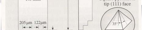
20 Geometry of PZT scanner Tb Tube scanner The tripod Not stable The outer electrode is segmented in four equal sectors of 90 degrees The inner electrode is driven by the z signal Bipolar configuration Δ x = KΔV, K ~ 3nm / V Model Scan Size Vertical Range A 0.4 μm 0.4 μm 0.4 μm E 10 μm 10 μm 2.5 μm J 125 μm 125 μm 5 μm
21 Triangular pattern Fast scan speed v f = 2lv Hz Slow scan speed v s = l v N Hz Fast scan direction
22 Feedback loop
23 AFM Probe Construction Low spring constant (k to 10 2 N/m) Sharp protruding tip (r=5-50 nm) High resonance frequency enc ω = 1 2ππ k m Three common types of AFM tip normal supertip ultralever


24 Common types of cantilevers Si 3 N 4 Si Diamond
25 Fabrication of cantilevers


 ' Zt ks")
26 Calibration of cantilever Theoretical method Static method Dynamic method Measuring of thermal response of the cantilever Measuring of the change of resonance frequency caused by the addition of known masses ( Z ) ' Zt ks = Ztkc t
27 How do I measure k? first, measure the resonance response of the cantilever using an AFM (if you are used to working in an AC mode such as tapping, you already know how to do this.) second, attach a spherical particle to the cantilever. Make sure you know what the particle is made of, since you want to be able to calculate l its mass. third, take an SEM image of the whole cantilever top down to measure the dimensions. In the same session take an image of a calibration grid so you really know. Take an image of the sphere and measure its diameter. Take a side view and measure the thickness of the cantilever (This is critical as k is proportional to the cube of the thickness!) fourth, remeasure the resonance response of the cantilever. Now you have heaps of data with which to determine k.


28 Superposition of two geometries


29 Reconvolution of the tip shape I II r d D=d real d D 2 D = 4 r
30 Calibration of the tip shape 2r L L 2 2 L L R = R = 4r 2 h h
31 Useful formulas 2 d Δz = 8R d 2. 8nm Δz = d > 3nm d 2 ( 4d + 8R ) d ( ) = 2 R Δ z + Δz + Δh
32 Oxide-Sharpened Tips increasing g aspect ratio reducing tip radius SiO 2 HF etching Aspect ration- 10:1 Radius r~1nm
33 Electron beam deposition (EBD) High-aspect-ratio tips L=(1-5)μm R=(20-40)nm Carbon materials are deposed by the dissociation of Carbon materials are deposed by the dissociation of background gases in the SEM vacuum chamber
, d=(0.")
 (nested, concentrically")

 Buckled nanotubes Labor")
34 Carbon Nanotube Tips Single-walled carbon nanotubes (SWNT), d=(0.7-3)nm Multiwalled carbon nanotubes (MWNT) (nested, concentrically arranged SWNT, d=(3-50)nm High-aspect-ration AFM probes Very stiff, E=10 12 Pa (the stiffest known materials) Buckled nanotubes Labor intensive Not t amenable to mass production
35 Pick-up Tips d=0.9nm d=2.8nm
")


 Presipitates")
36 Chemical Vapor deposition (CVD) Direct grow nanotubes onto AFM tip Heating of nanocatalyst particle (r~3.5 nm) Presipitates carbon nucleates a grow of nanotube


37 Direct grow of nanotubes Alumina/iron/molybdenumpowdered catalyst 2 nm in diameter 2μm in length
Outline Scanning Probe Microscope (SPM)
") AFM Outline Scanning Probe Microscope (SPM) A family of microscopy forms where a sharp probe is scanned across a surface and some tip/sample interactions are monitored Scanning Tunneling Microscopy (STM)
AFM Outline Scanning Probe Microscope (SPM) A family of microscopy forms where a sharp probe is scanned across a surface and some tip/sample interactions are monitored Scanning Tunneling Microscopy (STM)
Lecture 4 Scanning Probe Microscopy (SPM)
") Lecture 4 Scanning Probe Microscopy (SPM) General components of SPM; Tip --- the probe; Cantilever --- the indicator of the tip; Tip-sample interaction --- the feedback system; Scanner --- piezoelectric
Lecture 4 Scanning Probe Microscopy (SPM) General components of SPM; Tip --- the probe; Cantilever --- the indicator of the tip; Tip-sample interaction --- the feedback system; Scanner --- piezoelectric
Addition 1. Shear Stack Piezoelectric Elements and Shear Effect Basics
 120 Addition 1 Shear Stack Piezoelectric Elements and Shear Effect Basics Introduction The STM scanner built up in this work is a Besocke type scanner (see room temperature STM instrumental chapter). The
Instrumentation and Operation
 Instrumentation and Operation 1 STM Instrumentation COMPONENTS sharp metal tip scanning system and control electronics feedback electronics (keeps tunneling current constant) image processing system data
INTRODUCTION TO SCA\ \I\G TUNNELING MICROSCOPY
 INTRODUCTION TO SCA\ \I\G TUNNELING MICROSCOPY SECOND EDITION C. JULIAN CHEN Department of Applied Physics and Applied Mathematics, Columbia University, New York OXFORD UNIVERSITY PRESS Contents Preface
Classification of Dielectrics & Applications
 Classification of Dielectrics & Applications DIELECTRICS Non-Centro- Symmetric Piezoelectric Centro- Symmetric Pyroelectric Non- Pyroelectric Ferroelectrics Non-Ferroelectric Piezoelectric Effect When
Piezo materials. Actuators Sensors Generators Transducers. Piezoelectric materials may be used to produce e.g.: Piezo materials Ver1404
 Noliac Group develops and manufactures piezoelectric materials based on modified lead zirconate titanate (PZT) of high quality and tailored for custom specifications. Piezoelectric materials may be used
Introduction to Scanning Tunneling Microscopy
 Introduction to Scanning Tunneling Microscopy C. JULIAN CHEN IBM Research Division Thomas J. Watson Research Center Yorktown Heights, New York New York Oxford OXFORD UNIVERSITY PRESS 1993 CONTENTS List
Scanning Probe Microscopy. Amanda MacMillan, Emmy Gebremichael, & John Shamblin Chem 243: Instrumental Analysis Dr. Robert Corn March 10, 2010
 Scanning Probe Microscopy Amanda MacMillan, Emmy Gebremichael, & John Shamblin Chem 243: Instrumental Analysis Dr. Robert Corn March 10, 2010 Scanning Probe Microscopy High-Resolution Surface Analysis
And Manipulation by Scanning Probe Microscope
 Basic 15 Nanometer Scale Measurement And Manipulation by Scanning Probe Microscope Prof. K. Fukuzawa Dept. of Micro/Nano Systems Engineering Nagoya University I. Basics of scanning probe microscope Basic
Scanning Force Microscopy
 Scanning Force Microscopy Roland Bennewitz Rutherford Physics Building 405 Phone 398-3058 roland.bennewitz@mcgill.ca Scanning Probe is moved along scan lines over a sample surface 1 Force Microscopy Data
Scanning Tunneling Microscopy
 Scanning Tunneling Microscopy A scanning tunneling microscope (STM) is an instrument for imaging surfaces at the atomic level. Its development in 1981 earned its inventors, Gerd Binnig and Heinrich Rohrer
MS482 Materials Characterization ( 재료분석 ) Lecture Note 11: Scanning Probe Microscopy. Byungha Shin Dept. of MSE, KAIST
 Lecture Note 11: Scanning Probe Microscopy. Byungha Shin Dept. of MSE, KAIST") 2015 Fall Semester MS482 Materials Characterization ( 재료분석 ) Lecture Note 11: Scanning Probe Microscopy Byungha Shin Dept. of MSE, KAIST 1 Course Information Syllabus 1. Overview of various characterization
2015 Fall Semester MS482 Materials Characterization ( 재료분석 ) Lecture Note 11: Scanning Probe Microscopy Byungha Shin Dept. of MSE, KAIST 1 Course Information Syllabus 1. Overview of various characterization
ESO 205 Nature and Properties of Materials
 Dielectric Materials Topics to discuss Principles of dielectrics Dielectrics Loss and Breakdown Polarizations Frequency dependence Ferro-, Piezo- and Pyro- electrics ESO 205 Nature and Properties of Materials
General concept and defining characteristics of AFM. Dina Kudasheva Advisor: Prof. Mary K. Cowman
 General concept and defining characteristics of AFM Dina Kudasheva Advisor: Prof. Mary K. Cowman Overview Introduction History of the SPM invention Technical Capabilities Principles of operation Examples
Principles of Active Vibration Control: Piezoelectric materials
 Principles of Active Vibration Control: Piezoelectric materials Introduction: Piezoelectric materials are materials that produce a voltage when stress is applied. Since, this effect also applies in the
Piezo Theory: Chapter 1 - Physics & Design
 Piezoelectric effect inverse piezoelectric effect The result of external forces to a piezoelectric material is positive and negative electrical charges at the surface of the material. If electrodes are
Institute for Electron Microscopy and Nanoanalysis Graz Centre for Electron Microscopy
 Institute for Electron Microscopy and Nanoanalysis Graz Centre for Electron Microscopy Micromechanics Ass.Prof. Priv.-Doz. DI Dr. Harald Plank a,b a Institute of Electron Microscopy and Nanoanalysis, Graz
PIEZOELECTRIC TECHNOLOGY PRIMER
 PIEZOELECTRIC TECHNOLOGY PRIMER James R. Phillips Sr. Member of Technical Staff CTS Wireless Components 4800 Alameda Blvd. N.E. Albuquerque, New Mexico 87113 Piezoelectricity The piezoelectric effect is
Piezoelectricity: Basics and applications. Friday Morning Meeting, Technical Talk Petar Jurcevic
 Piezoelectricity: Basics and applications Friday Morning Meeting, 30.07.2010 Technical Talk Petar Jurcevic 1 Overview -A simple molecular model -Mathematical modelling -Some general notes -Overview Motors
(Scanning Probe Microscopy)
") (Scanning Probe Microscopy) Ing-Shouh Hwang (ishwang@phys.sinica.edu.tw) Institute of Physics, Academia Sinica, Taipei, Taiwan References 1. G. Binnig, H. Rohrer, C. Gerber, and Weibel, Phys. Rev. Lett.
(Scanning Probe Microscopy) Ing-Shouh Hwang (ishwang@phys.sinica.edu.tw) Institute of Physics, Academia Sinica, Taipei, Taiwan References 1. G. Binnig, H. Rohrer, C. Gerber, and Weibel, Phys. Rev. Lett.
COURSE OUTLINE. Introduction Signals and Noise Filtering Sensors: Piezoelectric Force Sensors. Sensors, Signals and Noise 1
 Sensors, Signals and Noise 1 COURSE OUTLINE Introduction Signals and Noise Filtering Sensors: Piezoelectric Force Sensors Piezoelectric Force Sensors 2 Piezoelectric Effect and Materials Piezoelectric
Program Operacyjny Kapitał Ludzki SCANNING PROBE TECHNIQUES - INTRODUCTION
 Program Operacyjny Kapitał Ludzki SCANNING PROBE TECHNIQUES - INTRODUCTION Peter Liljeroth Department of Applied Physics, Aalto University School of Science peter.liljeroth@aalto.fi Projekt współfinansowany
Lecture 6: Piezoelectricity & Piezoresistivity
 Lecture 6: Piezoelectricity & Piezoresistivity The Piezoelectric Effect Some crystal would electrically polarize when deformed by an applied force. When equal and opposite forces F 1 and F 2 (generating
Characterization of MEMS Devices
 MEMS: Characterization Characterization of MEMS Devices Prasanna S. Gandhi Assistant Professor, Department of Mechanical Engineering, Indian Institute of Technology, Bombay, Recap Characterization of MEMS
5. Building Blocks I: Ferroelectric inorganic micro- and nano(shell) tubes
 tubes") 5. Building Blocks I: Ferroelectric inorganic micro- and nano(shell) tubes 5.1 New candidates for nanoelectronics: ferroelectric nanotubes In this chapter, one of the core elements for a complex building
5. Building Blocks I: Ferroelectric inorganic micro- and nano(shell) tubes 5.1 New candidates for nanoelectronics: ferroelectric nanotubes In this chapter, one of the core elements for a complex building
Scanning Tunneling Microscopy
 Scanning Tunneling Microscopy References: 1. G. Binnig, H. Rohrer, C. Gerber, and Weibel, Phys. Rev. Lett. 49, 57 (1982); and ibid 50, 120 (1983). 2. J. Chen, Introduction to Scanning Tunneling Microscopy,
Introduction to solid state physics
 PHYS 342/555 Introduction to solid state physics Instructor: Dr. Pengcheng Dai Professor of Physics The University of Tennessee (Room 407A, Nielsen, 974-1509) Chapter 13: Dielectrics and ferroelectrics
Introduction to Scanning Probe Microscopy
 WORKSHOP Nanoscience on the Tip Introduction to Scanning Probe Microscopy Table of Contents: 1 Historic Perspectives... 1 2 Scanning Force Microscopy (SFM)... 2 2.1. Contact Mode... 2 2.2. AC Mode Imaging...
Piezoactuators. Jiří Tůma
 Piezoactuators Jiří Tůma 1 Domain Piezoelectric effect Direct piezoelectric effect discovered the brothers Pierre and Jacques Curie. They found that certain crystalline materials (ceramics) having the
Scanning Tunneling Microscopy
 Scanning Tunneling Microscopy References: 1. G. Binnig, H. Rohrer, C. Gerber, and Weibel, Phys. Rev. Lett. 49, 57 (1982); and ibid 50, 120 (1983). 2. J. Chen, Introduction to Scanning Tunneling Microscopy,
7.Piezoelectric, Accelerometer and Laser Sensors
 7.Piezoelectric, Accelerometer and Laser Sensors 7.1 Piezoelectric sensors: (Silva p.253) Piezoelectric materials such as lead-zirconate-titanate (PZT) can generate electrical charge and potential difference
Dielectric Properties of Solids
 Dielectric Properties of Solids Electric polarization In an insulator the electrons are so tightly bound that at ordinary temperatures they cannot be dislodged either by thermal vibrations or with ordinary
3.052 Nanomechanics of Materials and Biomaterials Thursday 02/15/07 Prof. C. Ortiz, MIT-DMSE I LECTURE 4: FORCE-DISTANCE CURVES
 I LECTURE 4: FORCE-DISTANCE CURVES Outline : LAST TIME : ADDITIONAL NANOMECHANICS INSTRUMENTATION COMPONENTS... 2 PIEZOS TUBES : X/Y SCANNING... 3 GENERAL COMPONENTS OF A NANOMECHANICAL DEVICE... 4 HIGH
SENSORS and TRANSDUCERS
 SENSORS and TRANSDUCERS Tadeusz Stepinski, Signaler och system The Mechanical Energy Domain Physics Surface acoustic waves Silicon microresonators Variable resistance sensors Piezoelectric sensors Capacitive
User s Manual. STUDY OF DIELECTRIC CONSTANT Model: DEC-01
 User s Manual STUDY OF DIELECTRIC CONSTANT Model: DEC-01 Manufactured by.. Scientific Equipment & Services 358/1, New Adarsh Nagar, Roorkee - 247 667, UA, INDIA Ph.: +91-1332-272852, 277118 Fax: +91-1332-274831
Integrating MEMS Electro-Static Driven Micro-Probe and Laser Doppler Vibrometer for Non-Contact Vibration Mode SPM System Design
 Tamkang Journal of Science and Engineering, Vol. 12, No. 4, pp. 399 407 (2009) 399 Integrating MEMS Electro-Static Driven Micro-Probe and Laser Doppler Vibrometer for Non-Contact Vibration Mode SPM System
Ferroelectric Ceramic Technology for Sensors. Jim McIntosh Ceramic Operations Manager PCB Piezotronics
 Ferroelectric Ceramic Technology for Sensors Jim McIntosh Ceramic Operations Manager PCB Piezotronics Overview Ferroelectricity versus Piezoelectricity Historical Background Ferroelectric Ceramic Composition
REPORT ON SCANNING TUNNELING MICROSCOPE. Course ME-228 Materials and Structural Property Correlations Course Instructor Prof. M. S.
 REPORT ON SCANNING TUNNELING MICROSCOPE Course ME-228 Materials and Structural Property Correlations Course Instructor Prof. M. S. Bobji Submitted by Ankush Kumar Jaiswal (09371) Abhay Nandan (09301) Sunil
Contents. What is AFM? History Basic principles and devices Operating modes Application areas Advantages and disadvantages
 Contents What is AFM? History Basic principles and devices Operating modes Application areas Advantages and disadvantages Figure1: 2004 Seth Copen Goldstein What is AFM? A type of Scanning Probe Microscopy
STM: Scanning Tunneling Microscope
 STM: Scanning Tunneling Microscope Basic idea STM working principle Schematic representation of the sample-tip tunnel barrier Assume tip and sample described by two infinite plate electrodes Φ t +Φ s =
MME 467: Ceramics for Advanced Applications
 MME 467: Ceramics for Advanced Applications Lecture 26 Dielectric Properties of Ceramic Materials 2 1. Barsoum, Fundamental Ceramics, McGraw-Hill, 2000, pp.513 543 2. Richerson, Modern Ceramic Engineering,
SCANNING-PROBE TECHNIQUES OR APPARATUS; APPLICATIONS OF SCANNING-PROBE TECHNIQUES, e.g. SCANNING PROBE MICROSCOPY [SPM]
![SCANNING-PROBE TECHNIQUES OR APPARATUS; APPLICATIONS OF SCANNING-PROBE TECHNIQUES, e.g. SCANNING PROBE MICROSCOPY [SPM]](/thumbs/81/83165631.jpg "SCANNING-PROBE TECHNIQUES OR APPARATUS; APPLICATIONS OF SCANNING-PROBE TECHNIQUES, e.g. SCANNING PROBE MICROSCOPY [SPM]") G01Q SCANNING-PROBE TECHNIQUES OR APPARATUS; APPLICATIONS OF SCANNING-PROBE TECHNIQUES, e.g. SCANNING PROBE MICROSCOPY [SPM] Scanning probes, i.e. devices having at least a tip of nanometre sized dimensions
G01Q SCANNING-PROBE TECHNIQUES OR APPARATUS; APPLICATIONS OF SCANNING-PROBE TECHNIQUES, e.g. SCANNING PROBE MICROSCOPY [SPM] Scanning probes, i.e. devices having at least a tip of nanometre sized dimensions
Chap. 7. Dielectric Materials and Insulation
 Chap. 7. Dielectric Materials and Insulation - The parallel plate capacitor with free space as an insulator: - The electric dipole moment for a pair of opposite changes +Q and -Q separated by a finite
The interpretation of STM images in light of Tersoff and Hamann tunneling model
 The interpretation of STM images in light of Tersoff and Hamann tunneling model The STM image represents contour maps of constant surface LDOS at E F, evaluated at the center of the curvature of the tip.
Application of electrostatic force microscopy in nanosystem diagnostics
 Materials Science, Vol., No. 3, 003 Application of electrostatic force microscopy in nanosystem diagnostics TEODOR P. GOTSZALK *, PIOTR GRABIEC, IVO W. RANGELOW 3 Fulty of Microsystem Electronics and Photonics,
10 Measurement of Acceleration, Vibration and Shock Transducers
 Chapter 10: Acceleration, Vibration and Shock Measurement Dr. Lufti Al-Sharif (Revision 1.0, 25/5/2008) 1. Introduction This chapter examines the measurement of acceleration, vibration and shock. It starts
Chapter 10. Nanometrology. Oxford University Press All rights reserved.
 Chapter 10 Nanometrology Oxford University Press 2013. All rights reserved. 1 Introduction Nanometrology is the science of measurement at the nanoscale level. Figure illustrates where nanoscale stands
2.76/2.760 Multiscale Systems Design & Manufacturing
 2.76/2.760 Multiscale Systems Design & Manufacturing Fall 2004 MOEMS Devices for Optical communications system Switches and micromirror for Add/drops Diagrams removed for copyright reasons. MOEMS MEMS
CHARACTERIZATION of NANOMATERIALS KHP
 CHARACTERIZATION of NANOMATERIALS Overview of the most common nanocharacterization techniques MAIN CHARACTERIZATION TECHNIQUES: 1.Transmission Electron Microscope (TEM) 2. Scanning Electron Microscope
Creation of DIPOLE (two poles) (distortion of crystal structure by the small displacement of the ion in direction of electric field)
 (distortion of crystal structure by the small displacement of the ion in direction of electric field)") Dielectricity Dielectric materials: Materials which is generally insulators. Under applied electric field, there is a tiny movement of charge inside the material. Electric field Creation of DIPOLE (two
Dielectricity Dielectric materials: Materials which is generally insulators. Under applied electric field, there is a tiny movement of charge inside the material. Electric field Creation of DIPOLE (two
Experimental methods in physics. Local probe microscopies I
 Experimental methods in physics Local probe microscopies I Scanning tunnelling microscopy (STM) Jean-Marc Bonard Academic year 09-10 1. Scanning Tunneling Microscopy 1.1. Introduction Image of surface
Contactless Excitation of MEMS Resonant Sensors by Electromagnetic Driving
 Presented at the COMSOL Conference 2009 Milan University of Brescia Department of Electronics for Automation Contactless Excitation of MEMS Resonant Sensors by Electromagnetic Driving Marco Baù, VF V.
Piezo Engineering Primer
 . The Direct and Inverse Piezoelectric Effect In 88, while performing experiments with tourmaline, quartz, topaz, cane sugar and Rochelle salt crystals, Pierre and Jacques Curie discovered that when mechanical
Imaging Methods: Scanning Force Microscopy (SFM / AFM)
") Imaging Methods: Scanning Force Microscopy (SFM / AFM) The atomic force microscope (AFM) probes the surface of a sample with a sharp tip, a couple of microns long and often less than 100 Å in diameter.
Imaging Methods: Scanning Force Microscopy (SFM / AFM) The atomic force microscope (AFM) probes the surface of a sample with a sharp tip, a couple of microns long and often less than 100 Å in diameter.
672 Advanced Solid State Physics. Scanning Tunneling Microscopy
 672 Advanced Solid State Physics Scanning Tunneling Microscopy Biao Hu Outline: 1. Introduction to STM 2. STM principle & working modes 3. STM application & extension 4. STM in our group 1. Introduction
Piezoelectric Actuator for Micro Robot Used in Nanosatellite
 Piezoelectric Actuator for Micro Robot Used in Nanosatellite R Bansevicius, S Navickaite, V Jurenas and A Bubulis PIEZOELECTRIC ACTUATOR FOR MICRO ROBOT USED IN NANOSATELLITE. R Bansevicius 1, S Navickaite,
Piezoline. Introduction Instruction for Using 62 PIEZOLINE. Contents
 62 PIEZOLINE Piezoline Contents Introduction Instruction for using 62 Sealings 62 Piezoelectric actuators 63 1 Piezoelectric Effect inverse piezoelectric effect 64 2 Design of piezoactuators 64 2.1 Piezo
Scanning Probe Microscopy (SPM)
") CHEM53200: Lecture 9 Scanning Probe Microscopy (SPM) Major reference: 1. Scanning Probe Microscopy and Spectroscopy Edited by D. Bonnell (2001). 2. A practical guide to scanning probe microscopy by Park
CHEM53200: Lecture 9 Scanning Probe Microscopy (SPM) Major reference: 1. Scanning Probe Microscopy and Spectroscopy Edited by D. Bonnell (2001). 2. A practical guide to scanning probe microscopy by Park
Piezoelectric materials for MEMS applications Hiroshi Funakubo Tokyo Institute of Technology
 Piezoelectric materials for MEMS applications Hiroshi Funakubo Tokyo Institute of Technology MEMS Engineer Forum 2016/5/11 11:50-12:15 Content 1. Introduction 2. Processing 3. Materials Matter Content
Solid State Physics (condensed matter): FERROELECTRICS
: FERROELECTRICS") Solid State Physics (condensed matter): FERROELECTRICS Prof. Igor Ostrovskii The University of Mississippi Department of Physics and Astronomy Oxford, UM: May, 2012 1 People: Solid State Physics Condensed
Solid State Physics (condensed matter): FERROELECTRICS Prof. Igor Ostrovskii The University of Mississippi Department of Physics and Astronomy Oxford, UM: May, 2012 1 People: Solid State Physics Condensed
SENSOR DEVICES MECHANICAL SENSORS
 SENSOR DEVICES MECHANICAL SENSORS OUTLINE 4 Mechanical Sensors Introduction General mechanical properties Piezoresistivity Piezoresistive sensors Capacitive sensors Applications INTRODUCTION MECHANICAL
Scanning Probe Microscopy. EMSE-515 F. Ernst
 Scanning Probe Microscopy EMSE-515 F. Ernst 1 Literature 2 3 Scanning Probe Microscopy: The Lab on a Tip by Ernst Meyer,Ans Josef Hug,Roland Bennewitz 4 Scanning Probe Microscopy and Spectroscopy : Theory,
Transducers. EEE355 Industrial Electronics
 Transducers EEE355 Industrial Electronics 1 Terminology Transducers convert one form of energy into another Sensors/Actuators are input/output transducers Sensors can be passive (e.g. change in resistance)
Atomic and molecular interactions. Scanning probe microscopy.
 Atomic and molecular interactions. Scanning probe microscopy. Balázs Kiss Nanobiotechnology and Single Molecule Research Group, Department of Biophysics and Radiation Biology 27. November 2013. 2 Atomic
Basic Laboratory. Materials Science and Engineering. Atomic Force Microscopy (AFM)
") Basic Laboratory Materials Science and Engineering Atomic Force Microscopy (AFM) M108 Stand: 20.10.2015 Aim: Presentation of an application of the AFM for studying surface morphology. Inhalt 1.Introduction...
Basic Laboratory Materials Science and Engineering Atomic Force Microscopy (AFM) M108 Stand: 20.10.2015 Aim: Presentation of an application of the AFM for studying surface morphology. Inhalt 1.Introduction...
Finite Element Analysis of Piezoelectric Cantilever
 Finite Element Analysis of Piezoelectric Cantilever Nitin N More Department of Mechanical Engineering K.L.E S College of Engineering and Technology, Belgaum, Karnataka, India. Abstract- Energy (or power)
Piezoelectric Resonators ME 2082
 Piezoelectric Resonators ME 2082 Introduction K T : relative dielectric constant of the material ε o : relative permittivity of free space (8.854*10-12 F/m) h: distance between electrodes (m - material
Lecture 26 MNS 102: Techniques for Materials and Nano Sciences
 Lecture 26 MNS 102: Techniques for Materials and Nano Sciences Reference: #1 C. R. Brundle, C. A. Evans, S. Wilson, "Encyclopedia of Materials Characterization", Butterworth-Heinemann, Toronto (1992),
Chapter 2 Scanning probes microscopes instrumentation. Chapter 2 Scanning probes microscopes instrumentation. 2.1: Tips. STM tips: requirements
 Chapter Objective: learn the general techniques that are essential for SPM. Chapter.1: Tips STM tips: requirements Geometry: Need for atomically-sharp apex for atomic resolution on a flat surface, rest
Lecture 19. Measurement of Solid-Mechanical Quantities (Chapter 8) Measuring Strain Measuring Displacement Measuring Linear Velocity
 Measuring Strain Measuring Displacement Measuring Linear Velocity") MECH 373 Instrumentation and Measurements Lecture 19 Measurement of Solid-Mechanical Quantities (Chapter 8) Measuring Strain Measuring Displacement Measuring Linear Velocity Measuring Accepleration and
MECH 373 Instrumentation and Measurements Lecture 19 Measurement of Solid-Mechanical Quantities (Chapter 8) Measuring Strain Measuring Displacement Measuring Linear Velocity Measuring Accepleration and
ME 515 Mechatronics. Overview of Computer based Control System
 ME 515 Mechatronics Introduction to Sensors I Asanga Ratnaweera Department of Faculty of Engineering University of Peradeniya Tel: 081239 (3627) Email: asangar@pdn.ac.lk Overview of Computer based Control
NIS: what can it be used for?
 AFM @ NIS: what can it be used for? Chiara Manfredotti 011 670 8382/8388/7879 chiara.manfredotti@to.infn.it Skype: khiaram 1 AFM: block scheme In an Atomic Force Microscope (AFM) a micrometric tip attached
Micromechanical Instruments for Ferromagnetic Measurements
 Micromechanical Instruments for Ferromagnetic Measurements John Moreland NIST 325 Broadway, Boulder, CO, 80305 Phone:+1-303-497-3641 FAX: +1-303-497-3725 E-mail: moreland@boulder.nist.gov Presented at
Design And Analysis of Microcantilevers With Various Shapes Using COMSOL Multiphysics Software
 Design And Analysis of Microcantilevers With Various Shapes Using COMSOL Multiphysics Software V. Mounika Reddy 1, G.V.Sunil Kumar 2 1,2 Department of Electronics and Instrumentation Engineering, Sree
EE C247B / ME C218 INTRODUCTION TO MEMS DESIGN SPRING 2014 C. Nguyen PROBLEM SET #4
 Issued: Wednesday, Mar. 5, 2014 PROBLEM SET #4 Due (at 9 a.m.): Tuesday Mar. 18, 2014, in the EE C247B HW box near 125 Cory. 1. Suppose you would like to fabricate the suspended cross beam structure below
DESIGN AND FABRICATION OF THE MICRO- ACCELEROMETER USING PIEZOELECTRIC THIN FILMS
 DESIGN AND FABRICATION OF THE MICRO- ACCELEROMETER USING PIEZOELECTRIC THIN FILMS JYH-CHENG YU and FU-HSIN LAI Department of Mechanical Engineering National Taiwan University of Science and Technology
Ferroelectric materials contain one or more polar axes along which a spontaneous
 Chapter 3 Ferroelectrics 3.1 Definition and properties Ferroelectric materials contain one or more polar axes along which a spontaneous polarization can be developed below the material s Curie temperature.
Nanomotion Precision Piezo Ceramic Motors
 Nanomotion Precision Piezo Ceramic Motors The Company Nanomotion was founded in 1992 Developed enabling technology for ultrasonic piezo-ceramic motors Entered the market in 1996, selling products to leading
Modelling of Different MEMS Pressure Sensors using COMSOL Multiphysics
 International Journal of Current Engineering and Technology E-ISSN 2277 4106, P-ISSN 2347 5161 2017 INPRESSCO, All Rights Reserved Available at http://inpressco.com/category/ijcet Research Article Modelling
Epitaxial piezoelectric heterostructures for ultrasound micro-transducers
 15 th Korea-U.S. Forum on Nanotechnology Epitaxial piezoelectric heterostructures for ultrasound micro-transducers Seung-Hyub Baek Center for Electronic Materials Korea Institute of Science and Technology
Electrical material properties
 Electrical material properties U = I R Ohm s law R = ρ (l/a) ρ resistivity l length σ = 1/ρ σ conductivity A area σ = n q μ n conc. of charge carriers q their charge μ their mobility μ depends on T, defects,
Solid State Science and Technology, Vol. 13, No 1 & 2 (2005) ISSN
 ISSN") FABRICATION OF Bi-Ti-O THIN FILM PRESSURE SENSOR PREPARED BY ELECTRON BEAM EVAPORATION METHOD Chong Cheong Wei, Muhammad Yahaya and Muhamad Mat Salleh Institue of Microengineering and Nanoelectronics,
FABRICATION OF Bi-Ti-O THIN FILM PRESSURE SENSOR PREPARED BY ELECTRON BEAM EVAPORATION METHOD Chong Cheong Wei, Muhammad Yahaya and Muhamad Mat Salleh Institue of Microengineering and Nanoelectronics,
Outline. 4 Mechanical Sensors Introduction General Mechanical properties Piezoresistivity Piezoresistive Sensors Capacitive sensors Applications
 Sensor devices Outline 4 Mechanical Sensors Introduction General Mechanical properties Piezoresistivity Piezoresistive Sensors Capacitive sensors Applications Introduction Two Major classes of mechanical
Thin Film Bi-based Perovskites for High Energy Density Capacitor Applications
 ..SKELETON.. Thin Film Bi-based Perovskites for High Energy Density Capacitor Applications Colin Shear Advisor: Dr. Brady Gibbons 2010 Table of Contents Chapter 1 Introduction... 1 1.1 Motivation and Objective...
Atomic Force Microscopy (AFM) Part I
 Part I") Atomic Force Microscopy (AFM) Part I CHEM-L2000 Eero Kontturi 6 th March 2018 Lectures on AFM Part I Principles and practice Imaging of native materials, including nanocellulose Part II Surface force measurements
Atomic Force Microscopy (AFM) Part I CHEM-L2000 Eero Kontturi 6 th March 2018 Lectures on AFM Part I Principles and practice Imaging of native materials, including nanocellulose Part II Surface force measurements
INF5490 RF MEMS. LN03: Modeling, design and analysis. Spring 2008, Oddvar Søråsen Department of Informatics, UoO
 INF5490 RF MEMS LN03: Modeling, design and analysis Spring 2008, Oddvar Søråsen Department of Informatics, UoO 1 Today s lecture MEMS functional operation Transducer principles Sensor principles Methods
Polarization. D =e i E=k i e o E =e o E+ P
 Dielectrics Polarization a perfect insulator or a dielectric is the material with no free charge carriers. if an electric field, E, is applied to the insulator no charge flow. However in the presence of
Scanning tunneling microscopy
 IFM The Department of Physics, Chemistry and Biology Lab 72 in TFFM08 Scanning tunneling microscopy NAME PERS. - NUMBER DATE APPROVED Rev. Dec 2006 Ivy Razado Aug 2014 Tuomas Hänninen Contents 1 Introduction
Scanning Probe Microscopy
 1 Scanning Probe Microscopy Dr. Benjamin Dwir Laboratory of Physics of Nanostructures (LPN) Benjamin.dwir@epfl.ch PH.D3.344 Outline: Introduction: What is SPM, history STM AFM Image treatment Advanced
MCT151: Introduction to Mechatronics Lecture 10: Sensors & Transduction Mechanisms
 Faculty of Engineering MCT151: Introduction to Mechatronics Lecture 10: Sensors & Transduction Mechanisms Slides are borrowed from Dr. Mohamed Elshiekh lectures Types of sensors Sensors are considered
B) Single module (monolithic) but nested (serial) X and Y. Better response than A) but X and Y still work without "knowledge" of each other.
 Single module (monolithic) but nested (serial) X and Y. Better response than A) but X and Y still work without knowledge of each other.") Tutorial Piezoelectrics in Positioning Flatness of a NanoPositioning stage with active trajectory control is better than of 1 nanometer over a 100 x 100 µm scanning range. Different Ways of Designing Multi-Axis
Tutorial Piezoelectrics in Positioning Flatness of a NanoPositioning stage with active trajectory control is better than of 1 nanometer over a 100 x 100 µm scanning range. Different Ways of Designing Multi-Axis
Supplementary Methods A. Sample fabrication
 Supplementary Methods A. Sample fabrication Supplementary Figure 1(a) shows the SEM photograph of a typical sample, with three suspended graphene resonators in an array. The cross-section schematic is
Transduction Based on Changes in the Energy Stored in an Electrical Field
 Lecture 6- Transduction Based on Changes in the Energy Stored in an Electrical Field Actuator Examples Microgrippers Normal force driving In-plane force driving» Comb-drive device F = εav d 1 ε oε F rwv
Santosh Devasia Mechanical Eng. Dept., UW
 Nano-positioning Santosh Devasia Mechanical Eng. Dept., UW http://faculty.washington.edu/devasia/ Outline of Talk 1. Why Nano-positioning 2. Sensors for Nano-positioning 3. Actuators for Nano-positioning
Microelectromechanical systems (MEMS) have become an increasingly important area of
 have become an increasingly important area of") 1 Chapter 1 Introduction 1.1 Background Microelectromechanical systems (MEMS) have become an increasingly important area of technology. This is due to the premise that the efficiencies of high volume production
1 Chapter 1 Introduction 1.1 Background Microelectromechanical systems (MEMS) have become an increasingly important area of technology. This is due to the premise that the efficiencies of high volume production
Piezoelectric and Ferroelectric materials. Zaahir Salam
 Piezoelectric and Ferroelectric materials Zaahir Salam Some Basic Terms Dielectric Material- The Cumulative effect of microscopic displacements (charges,ions,electrons) results in Net Polarization due
Characterization of MEMS Devices
 MEMS: Characterization Characterization of MEMS Devices Prasanna S. Gandhi Assistant Professor, Department of Mechanical Engineering, Indian Institute of Technology, Bombay, Recap Fabrication of MEMS Conventional
3.1 Electron tunneling theory
 Scanning Tunneling Microscope (STM) was invented in the 80s by two physicists: G. Binnig and H. Rorher. They got the Nobel Prize a few years later. This invention paved the way for new possibilities in
INTRODUCTION TO PIEZO TRANSDUCERS
 PIEZO SYSTEMS, INC. 65 Tower Office Park Woburn, MA 01801 USA Tel: 781 933 4850 Fax: 781 933 4743 email: sales@piezo.com Find Search for a product or category HOME PRODUCTS CUSTOM OEM CATALOG TECHNICAL