Resistance switching memories are memristors
|
|
|
- Blaze Lyons
- 6 years ago
- Views:
Transcription
1 Appl Phys A (2011) 102: DOI /s Resistance switching memories are memristors Leon Chua Received: 17 November 2010 / Accepted: 22 December 2010 / Published online: 28 January 2011 The Author(s) This article is published with open access at Springerlink.com Abstract All 2-terminal non-volatile memory devices based on resistance switching are memristors, regardless of the device material and physical operating mechanisms. They all exhibit a distinctive fingerprint characterized by a pinched hysteresis loop confined to the first and the third quadrants of the v i plane whose contour shape in general changes with both the amplitude and frequency of any periodic sinewave-like input voltage source, or current source. In particular, the pinched hysteresis loop shrinks and tends to a straight line as frequency increases. Though numerous examples of voltage vs. current pinched hysteresis loops have been published in many unrelated fields, such as biology, chemistry, physics, etc., and observed from many unrelated phenomena, such as gas discharge arcs, mercury lamps, power conversion devices, earthquake conductance variations, etc., we restrict our examples in this tutorial to solidstate and/or nano devices where copious examples of published pinched hysteresis loops abound. In particular, we sampled arbitrarily, one example from each year between the years 2000 and 2010, to demonstrate that the memristor is a device that does not depend on any particular material, or physical mechanism. For example, we have shown that spin-transfer magnetic tunnel junctions are examples of memristors. We have also demonstrated that both bipolar and unipolar resistance switching devices are memristors. The goal of this tutorial is to introduce some fundamental circuit-theoretic concepts and properties of the memristor that are relevant to the analysis and design of non-volatile nano memories where binary bits are stored as resistances L. Chua ( ) Berkeley Department of EECS, University of California, Berkeley, CA 94720, USA chua@eecs.berkeley.edu Fax: manifested by the memristor s continuum of equilibrium states. Simple pedagogical examples will be used to illustrate, clarify, and demystify various misconceptions among the uninitiated. 1 Pinched hysteresis loops The memristor [1] is a 2-terminal circuit element characterized by a constitutive relation between two mathematical variables q and ϕ representing the time integral of the element s current i(t), and voltage v(t); namely, q(t) = t i(τ)dτ (1) t ϕ(t) = v(τ)dτ (2) It is important to stress that q and ϕ are defined mathematically and need not have any physical interpretations. Nevertheless, we call q the charge and ϕ the flux of the memristor since (1) and (2) coincide with the formula relating charge to current, and flux to voltage, respectively. We say the memristor is charge-controlled,orflux-controlled, if its constitutive relation can be expressed by ϕ =ˆϕ(q) (3) or q =ˆq(ϕ) (4) respectively, where ˆϕ(q) and ˆq(ϕ) are continuous and piecewise-differentiable functions 1 with bounded slopes. 1 A function is piecewise-differentiable if its derivative is uniquely defined everywhere except possibly at isolated points.
2 766 L. Chua Differentiating (3) and (4) with respect to time t, we obtain v = dϕ dt = d ˆϕ(q) dq = R(q)i (5) dq dt where R(q) = d ˆϕ(q) (6) dq is called the memristance 2 at q, and has the unit of Ohms ( ), and i = dq dt = d ˆq(ϕ) dϕ = G(ϕ)v (7) dϕ dt where G(ϕ) = d ˆq(ϕ) (8) dϕ is called the memductance at ϕ, and has the unit of Siemens (S). Observe that (5)and (6)can be interpreted as Ohm s law except that the resistance R(q) at any time t = t 0 depends on the entire past history of i(t) from t = to t = t 0. Similarly the memductance G(ϕ) in (8) depends on the entire past history of v(t) from t = to t = t 0. It follows from (5) that the charge-controlled memristor defined in (3) is equivalent to the charge-dependent Ohm s law v = R(q)i (9) where R(q) is just the slope of the curve ϕ =ˆϕ(q) at q. To show that (3) and (5) are equivalent representations, we can recover (3) by integrating both sides of (5) with respect to t: t t ϕ = v(τ)dτ = R ( q(τ) ) i(τ)dτ t = R ( q(τ) ) dq(τ) dτ dτ = = q(t) q( ) q(t) q( ) R ( q(τ) ) dq(τ) R(q)dq =ˆϕ(q) (10) It follows from (10) that ˆϕ(q) = R(q)dq (11) 2 Just as memristor is an acronym for memory resistor, memristance is an acronym for memory resistance. Similarly memductance is an acronym for memory conductance. Similarly, a flux-controlled memristor is equivalent to the flux-dependent Ohm s law i = G(ϕ)v (12) where ϕ(t) ˆq(ϕ) = G(ϕ) dϕ (13) ϕ( ) Example 1 Consider the charge-controlled memristor shown in Fig. 1(a) along with the memristor symbol in the upper left corner. The memristor constitutive relation, shown in red, is described analytically by a cubic polynomial ϕ = q q3 (14) Let us apply a sinusoidal current source (blue sine wave in Fig. 1(c)) defined by { i(t) = A sin ωt, t 0 (15) = 0, t <0 across this memristor, as shown in Fig. 1(c) for A = 1 and ω = 1. To determine the corresponding voltage response v(t) from the constitutive relation (14), we must calculate first the corresponding charge (shown in red in Fig. 1(c)). Assuming the initial charge q 0 = q(0) = 0, we obtain upon integrating (15) the following equation for q(t): t q(t) = A sin(ωτ)dτ = A [1 cos ωt], t 0 (16) 0 ω Substituting (16)into(14), we obtain the corresponding flux (shown in magenta in Fig. 1(d)) ϕ(t) = A [ ω (1 cos ωt) ( A 2 ] )(1 cos ωt) 2 (17) 3 Differentiating (17) with respect to t, we obtain ] v(t) = A [1 + A2 (1 cos ωt)2 sin ωt (18) ω2 Plotting the loci 3 of (i(t), v(t)) in the v i plane, via (15) and (18), we obtain the pinched hysteresis loop shown in Fig. 1(b) for A = 1 and ω = 1. The hysteresis occurs because the maxima and minima of the sinusoidal input current i(t) in Fig. 1(c) do not occur at the same time as the corresponding memristor voltage v(t) in Fig. 1(d). The pinching attheorigininfig.1(b) occurs because both i(t) and v(t) become zero at the same time. To show that the hysteresis 3 Also known as a Lissajous figure. ω 2
3 Resistance switching memories are memristors 767 Fig. 1 Memristor symbol, constitutive relation, and pinched hysteresis loop associated with (v(t), i(t)) plotted for A = 1andω = 1. (a) Memristor symbol and ϕ =ˆϕ(q) characteristic curve. (b) Pinched hysteresis loop: double-valued Lissajous figure of (v(t), i(t)) for all times t except when it passes through the origin, where the loop is pinched. (c) Periodic waveforms associated with i(t) and q(t) = t 0 i(τ)dτ plotted with A = 1andω = 1. (d) Periodic waveforms associated with v(t) and ϕ(t) = t 0 v(τ)dτ loop is always pinched at the origin (v, i) = (0, 0), let us calculate the memristance R(q) from (6) and (14): R(q) = d ˆϕ(q) dq = 1 + q 2 (19) Substituting q(t) from (16)into(19), we obtain R ( q(t) ) [ ] A 2 = 1 + (1 cos ωt), t 0 (20) ω Observe from (19) and Fig. 2(c) that R(q) > 0 (21) Substituting (20) and (15)in(9), we obtain the same expression for the memristor voltage v(t) derived earlier in (18). Now since R(q) is finite for all finite q, it follows that v(t) = 0 whenever i(t) = 0 (22) for any input current i(t). Similarly, for any ϕ-controlled memristor whose memductance G(ϕ) is finite for all finite ϕ, wehave i(t) = 0 whenever v(t) = 0 (23) for any input voltage v(t). The waveform of R(t) givenby (20) is shown in Fig. 2(d) for A = 1 and ω = 1. The loci traced out by (R(t), i(t)) is shown in Fig. 2(b). Again we obtain a hysteresis loop, but it is not pinched since R(t) > 0 for all times. It is important to observe from Fig. 1(d) and Fig. 2(d) that while v(t) and i(t) assume both positive and negative values, both ϕ(t) and q(t) are non-negative. It follows that only the memristor ϕ q curve in the first quadrant is visited during every period of i(t). Observe also that the pinched hysteresis loop in Fig. 1(b) is odd symmetric with respect to the origin. Finally, observe that except for the memristor constitutive relation ϕ =ˆϕ(q) in Fig. 1(a), and its associated memristance R(q) in Fig. 2(c), which remain unchanged, all other waveforms of Figs. 1 and 2 will change when we vary the amplitude A or the frequency ω of the input signal i(t) = A sin ωt. In particular, note from (16) and (17) that q(t) 0 and ϕ(t) 0asω. This makes perfect sense since as we increase the frequency ω of the sinusoidal input current i(t) = A sin ωt, while keeping the amplitude constant, the area accumulated from t = 0 to the first half period t = π ω diminishes with ω. It follows therefore that the memristance R(q(t)) R(0) = 1, as ω (24) We can confirm this prediction via (18) by noting that v(t) A sin ωt, as ω (25)
4 768 L. Chua Fig. 2 (a) Memristor constitutive relation. (b) Resistance hysteresis loop associated with (R(t), i(t)). (c) Memristance plotted as a function of q. (d) Periodic waveforms of i(t), q(t), v(t), andr(t), plotted for A = 1, ω = 1 In fact, this is one of the signature properties of a memristor, which we formalize as follows: Memristor pinched hysteresis loop fingerprint The loci (Lissajous figure) in the v i plane of any passive memristor with positive memristance R(q) = d ˆϕ(q) > 0 (26) dq and driven by a sinusoidal current source i(t) = A sin ωt is always a pinched hysteresis loop, whose area shrinks with frequency and tends to a linear resistance equal to R(0) = slope of the constitutive relation ϕ =ˆϕ(q) at q = 0. We remark here that there exist degenerate cases where the v i Lissajous figure is a single-valued function, such as the example shown in Fig. 3 when we drive the same memristor from Fig. 1 with the special input i(t) = cos t for t 0. In fact, we can interpret the loci shown in Fig. 3(b) as a degenerate case where the hysteresis loop collapsed into a single-valued function, passing through the origin. Hence, the loci is still pinched, even in this degenerate scenario. Another degenerate scenario can occur when the slope R(q) = 0 at some points on ϕ =ˆϕ(q) function, as illustrated in Fig. 4 for the constitutive relation ϕ = 1 3 q3 (27) In this case R(0) = 0. For the same input current source i(t) = cos t as in Fig. 3, we obtain a single-valued functioninthev i plane which touches the i-axis, as shown in Fig. 4(b). This represents another degenerate situation where the v i Lissajous figure actually includes points on the i-axis, as it is impossible to cross the i-axis for any passive memristor where R(q) 0. 4 In such situations, the v i Lissajous figure must still pass through the origin (i.e., it is pinched), but it makes contact with the i-axis as well. In either case, the Lissajous figure (R(q) 0) of a passive memristor must be confined to the first and the third quadrants, including possibly the i-axis, of the v i plane [3]. 2 Continuum of non-volatile memories A cursory examination of the charge-controlled memristor constitutive relation ϕ = ˆϕ(q) in Fig. 2(a) shows that its memristance M(q) varies from 5 R(q 1 ) = 1 to, as depicted in the Resistance vs. charge curve in Fig. 2(c), henceforth called the Resistance vs. State map. InFig.2(c), charge is the state variable. 4 Note the preceding memristor fingerprint property is stated for the case R(q) > 0. 5 To avoid clutter, we will often write Memristance M(q) and Resistance R(q) interchangeably. Likewise, we will often write Conductance G(ϕ) for Memductance W(ϕ). Similarly, weusethetermsmemristance and resistance, as well as memductance and conductance, to mean the same thing.
5 Resistance switching memories are memristors 769 Fig. 3 Illustration of a degenerate scenario where the pinched hysteresis loop collapsed into a single-valued function when driven in this case with i(t) = cos t,withthe same ϕ =ˆϕ(q) constitutive relation as Fig. 1(a) Fig. 4 Example illustrating the second degenerate scenario where the Lissajous figure in the v i plane actually reaches the i-axis. This limiting case can occur when the memristor constitutive relation has R(q) = 0atsomeq, asin Fig. 4(a) where R(q) = 0at q = 0[3] The Resistance vs. State map is a very useful graph because it shows how to navigate from one memristance R 0 at state q = q 0 on the memristor ϕ vs. q curve to another memristance R 1 at state q = q 1 by simply applying a short current pulse i(t) whose area is equal to the increment q needed to be added to the latest value of q(t 0 ) = q 0 in order to move from R 0 to R 1. The memristance vs. state map in Fig. 2(c) therefore allows one to tune the memristor s resistance continuously from R = 1 to R =.
6 770 L. Chua It is important to observe that if one opens or short circuits a memristor having a resistance R 0 at t = t 0 so that the memristor is in equilibrium, i.e., v = 0, and i = 0, at t = t 0, the memristor does not lose the value of ϕ and q when both voltage v and current i become zero at the instant when the power is switched off, but rather holds the value unchanged at q 0 and ϕ 0, forever! Hence the passive memristor exhibits non-volatile memory. 3 ϕ q curve and memristance vs. state maps are equivalent memristor representations Both the ϕ vs. q constitutive relation (such as Fig. 2(a)) and its associated resistance vs. state map (such as Fig. 2(c)) with the state equation dq/dt = i are equivalent representations of a memristor in the sense that given any applied current source input signal i(t) for all times from t =, or equivalently, for positive times from t = 0, plus the initial charge q(0) which represents the time integral of i(t) from t = to t = 0, one can calculate the corresponding voltage v(t). Conversely, given any v(t), one can calculate the corresponding i(t), assuming R>0 so that the inverse constitutive relation q =ˆq(ϕ) is a continuous function. In contrast, all of the waveforms and hysteresis loops depicted in Figs. 1 and 2 are only manifestations of a memristor, and cannot be used to predict the voltage response given any other excitation waveforms different from the waveform i = A sin ωt, with A = 1 and ω = 1, in Fig. 1(c). The reader should verify that changing the parameter A,orω, or changing the waveforms of i(t) would result in completely different responses. For example, it follows from (16), (18) and (19) that if we hold the amplitude A = 1 while increasing the frequency ω, we would find that q(t) tends to zero, v(t) tends to sin t, and R(t) tends to 1, as the hysteresis loop in Fig. 1(b) shrinks until it collapses into a unit-slope straight line through the origin. Indeed, as ω tends to,the charge q(t), and flux ϕ(t) would both tend to the origin in Fig. 1(a), and remain motionless thereafter. Under this limiting situation, the memristor degenerates into a linear R resistor where R is just the slope of the ϕ q curve at the origin in Fig. 1(a); namely, R = 1. Memristorlesson1 Pinched hysteresis loops are not models! While a pinched v i hysteresis loop measured from an experimental 2-terminal device implies that the device is a memristor, the pinched loop itself is useless as a model since it cannot be used to predict the voltage response to arbitrarily applied current signals, and vice versa. The only way to predict the response of the device is to derive either the ϕ q constitutive relation,orthememristance vs. state map. 4 Resistance vs. state map and state equation When we write, or utter, the term resistance, orconductance, 6 we must always subconsciously remind ourselves that we are referring to a 2-terminal electrical device that obeys a linear equation called Ohm s law; namely, Ohm s law: v = Ri (28) where R is a constant, called the resistance of the resistor, where R has the unit of. It is conceptually important to distinguish between the two words resistance and resistor: resistor is a device, while resistance is the slope of the straight line defined by Ohm s law. No harm is done when the device is linear-hence the sloppiness in current usage. However, for nonlinear devices, it is crucial to distinguish them! The resistance vs. state map of a memristor also obeys Ohm s Law, except that the resistance R is not a constant, as illustrated by the example in Fig. 2(c), but depends on a dynamical state variable x (x = q in the ideal memristor case considered so far) which evolves according to a prescribed ordinary differential equation, called the state equation. An ideal memristor is therefore defined by: 7 State-dependent Ohm s law: v = R(x)i Memristor state equation: dx dt = i Memristorlesson2 (29a) (29b) A memristor is defined by a state-dependent Ohm s law. 5 Correspondence between small-signal memristance and chord memristance Let us apply a sinusoidal current source i(t) = A sin ωt across a charge-controlled memristor as in Fig. 1. The memristance R(q(t k )) at t = t k as calculated from (6) is equal to the slope of the ϕ q curve at q = q(t k ). The slope at q(t k ) will in general vary with the time-evolution of ϕ(t). 6 To avoid clutter, we usually write only the term resistance, or conductance, with the understanding, mutatis mutandis, that the same follows for the dual case. 7 We henceforth adopt the standard notation x to denote a state variable in mathematical system theory, wherex maybeavectorx = (x 1,x 2,...,x n ). This will be the case for many non-ideal memristors found in practice.
7 Resistance switching memories are memristors 771 However, we can keep the slope at q(t k ) approximately constant over time by choosing a sufficiently small amplitude A while fixing the frequency ω, assuming the ϕ q curve is continuous at q = q(t k ). Under this small-signal condition, the memristance, henceforth called the small-signal memristance, would be indistinguishable from that of a linear resistance, which obeys Ohm s Law with a constant resistance equal to R(t k ) at all times. It follows that by applying a short current pulse signal of appropriate height, we can tune the memristance over a continuous range of values without introducing a third terminal, and without applying a continuous supply of power via a biasing circuit. For the example shown in Fig. 2(c), any small-signal memristance greater than 1 can be easily programmed. In particular, observe that we have aligned the vertical axis of Figs. 2(a) and 2(c) so that the value of R (height of the resistance vs. state map) is equal to the slope of the ϕ q curve in Fig. 2(a) at the point (q(t k ), ϕ(t k )), i.e., both points must fall on the vertical projection line through q = q(t k ). In other words, the memristor can be designed to function as a non-volatile and continuously tunable resistance. Let us consider next the large-signal case where A 0, e.g. A = 1 and ω = 1,asshowninFig.2. In this case, a quick calculation using (17) shows that the flux ϕ(t) oscillates between ϕ = 0 and ϕ = 14/3,asshowninFig.1(d). The corresponding memristance calculated from (20) ranges from R = 1toR = 5, as shown in Fig. 2(d). The corresponding v i Lissajous figure is the pinched hysteresis loop shown in Fig. 1(b). At any time t = t k, the memristance is equal to R(t k ) = v(t k) i(t k ). This number can be interpreted simply as the slope of a straight line, i.e., a chord, connecting the origin to the point (i(t k ), v(t k )) in the i v plane. We will henceforth call this large-signal resistance at time t = t k the chord memristance at t = t k. 8 Observe that the chord memristance at t = t k is simply the memristance calculated from the pinched hysteresis loop in Fig. 1(b) at the point where t = t k. This number is equal to the slope of a corresponding point on the ϕ q curve in Fig. 1(a), traversed at the same time t = t k ; namely, the small-signal memristance calculated at the same point. In fact, had we plotted Fig. 1(a) and Fig. 1(b) on the same scale, the chord connecting the point (i(t k ), v(t k )) to the origin at t = t k will be parallel to a corresponding line drawn tangent to the ϕ q curve in Fig. 1(a). For example, at t = π 2,(i(π 2 ), v( π 2 )) = (1, 2), and the chord resistance is given by R( π 2 ) = 2/1 = 2, and the corresponding small-signal memristance is given by (19) for q( π 2 ) = 1, namely, R(π 2 ) = = 2, as predicted and shown in Fig. 2(c). Let us summarize the above results as follow. 8 The terminology chord resistance had been widely used by neurobiologists, including Hodgkin and Huxley [5], for similar geometrical interpretations. Small-signal and chord memristance correspondence property The large-signal chord memristance calculated at any point (i(t k ), v(t k )) at time t = t k of a pinched hysteresis loop in the v i plane is equal to the small-signal memristance at a corresponding point on the ϕ q curve traversed at the same time. In particular, the slope of the chord connecting (0, 0) to (i(t k ), v(t k )) is equal to the slope of the line drawn tangent to the ϕ q curve at the corresponding point (q(t k ), ϕ(t k )). Recall that the small-signal memristance R(q(t)) remains constant under any sufficiently small odd-symmetric periodic current input signals, such as i(t) = A sin ωt where i( t) = i(t) because every value of the state variable x (charge in Fig. 1)isastable equilibrium point 9 and because the memristor is locally passive when R(q) 0[3]. The local passivity property is essential for small-signal memristor circuit analysis to make sense because a locally active memristor [3] could give rise to oscillations, and even chaos [6]. In contrast to the small-signal memristance, which does not depend on the input waveform of i(t) other than it being sufficiently small, the chord memristance is always associated with a particular Lissajous figure, such as a pinched hysteresis loop corresponding to a periodic input signal. However, once the input current waveform is given, we can derive the associated pinched hysteresis loop, such as that showninfig.1(b) when i = A sin ωt with A = 1 and ω = 1. In this case, we can interpret the two limiting chord memristances associated with the two hysteretic branches through the origin. In particular, the chord memristance of the lower limiting branch is equal in value to the small-signal memristance at the origin of the ϕ q curve in Fig. 2(a), namely, R(0) = 1. This also follows upon substitution of q = 0in (19) at time t = 0. The second chord memristance associated with the limiting upper branch through the origin in Fig. 2(b) is associated with the small-signal memristance at the point q = q(π) = 2, namely, R(2) = 5. For the pinched hysteresis loop shown in Fig. 1(b), the chord memristance will sweep from the lower limit R(0) = 1 to the upper limit R(2) = 5 in a counterclockwise direction in the first quadrant during the first half cycle, and then reversing the sweep in a symmetrical manner in the 9 A state x = x 0 is said to be an equilibrium point of a dynamical circuit if dx(t) dt = 0atx = x 0.Itissaidtobelocally asymptotically stable if it always returns to its original position whenever subjected to small perturbations, such as a small current pulse. An equilibrium point is said to be stable if any drift from its original position due to any perturbationtothestatevariablex is confined to a neighborhood of radius of about the same size as that of the perturbation. In other words, it does not diverge to infinity, as would be the case for an unstable equilibrium point. Neither does it return to its original position, as would be the case if the equilibrium point is asymptotically stable [3].
8 772 L. Chua third quadrant during the second half cycle, resulting in an odd-symmetric pinched hysteresis loop. The motion of the chord memristance in the first quadrant of Fig. 1(b)issimilar to that of an automobile windshield wiper except that the length of the blade changes continuously in accordance to the square root of the sum of squares of i(t) and v(t), from t = 0tot = π in the v i plane. 6 Ideal memristor ϕ q curves for binary memories For digital computer applications requiring only two memory states, the memristor needs to exhibit only two sufficiently distinct equilibrium states R 0 and R 1 where R 0 R 1, and such that the high-resistance state R 0 can be easily switched to the low resistance state R 1, and vice versa, as fast as possible while consuming as little energy as possible. In contrast to conventional memories, the memristor does not dissipate any power except during the brief switching time intervals because v(t) = dϕ(t)/dt = 0, and i(t) = dq(t)/dt = 0 at both equilibrium states R 0 and R 1. Our goal in this section is to present two ideal memristors for mimicking two, among many, recently published resistance switching memories. Memristor switching memory 1 Figure 5 shows a charge-controlled memristor characterized by a 3-segment odd-symmetric ϕ q curve (Fig. 5(b)). This piecewise-linear function can be described by the equation ( ) 1 [ q ϕ = R 0 q + 2 (R ] 1 R 0 ) + B q B (30) where R 1 denotes the slope of the middle segment in Fig. 5(b), R 0 denotes the slope of the outer segments in Fig. 5(b), q = B denotes the left charge breakpoint in Fig. 5(b), and q = B denotes the right charge breakpoint in Fig. 5(b). The corresponding memristance function R(q) is derived by differentiating (30) with respect to q; namely, R(q) = R (R 1 R 0 ) [ sgn(q + B) sgn(q B) ] (31) where sgn(.) is defined by sgn x = 1, if x>0 = 1, if x<0 (32) A graph of the memristance vs. state map is shown in Fig. 5(d) for the parameter values R 0 = 6000 and R 1 = Applying the sinusoidal current source defined in (16) with A = 2Bω across the memristor, the corresponding memristor charge is given by q(t) = 2B(1 cos ωt), t > 0 = 0, t <0 (33) In this case, the memristor ϕ q curve in Fig. 5(b) traverses from q = 0att = 0toq = 4B at t = π ω. Observe that starting from q(0) = 0inFig.5(b) at t = 0, the memristor charge q(t) increases along the lower branch while maintaining a constant memristance value of R 1 until it reaches the right breakpoint at q = B where it switches abruptly to the upper branch and continues to increase, with the constant high memristance value of R 0, until it reaches the maximum value of q(t) = 4B at t = π ω corresponding to the end of the first half cycle of the sinusoidal current input i(t). The corresponding chord memristance also remains constant at R 1 before the breakpoint q = B, and at R 0 after the breakpoint. During the next half cycle, the memristor input current i(t) changes sign, and so does the corresponding memristor voltage v(t). The loci in Fig. 5(b) then retraces the same route from q = 4B with a constant memristance R 0 at t = π ω until it reaches the right breakpoint q = B again, where the memristance switches to R 1, and continues to decrease until it returns to the initial departure point q = 0att = 2 π ω. Since both i(t) and v(t) are negative during the return trip, the plot of the corresponding Lissajous figure in the v i plane is an odd-symmetric pinched hysteresis loop, as shown in Fig. 5(c). Observe that it consists of only two chord memristances equal to R 1 for the lower branch, and R 0 for the upper branch. Observe also that the switching occurs instantaneously, in both directions, in this case in view of the discontinuity in slope of the ϕ q curve at the two breakpoints q = B and q = B. The corresponding memristance vs. state map shown in Fig. 5(d) for R 1 = 2500, and R 0 = 6000, alsoshows a discontinuous jump at the same breakpoints, as expected. If we transcribe the corresponding loci of the memristance R(t) from the pinched hysteresis loop in Fig. 5(c) into the R vs. i plane, we would obtain the square resistance hysteresis loop shown in Fig. 5(e). This plot is the piecewise-linear analog of the smooth differentiable ϕ q curve in Fig. 2(b). A cursory glance at the figures from Ref. [7] reveals similarities in the respective rectangular resistance hysteresis loops. From a circuit-theoretic perspective, the non-volatile resistance switching memory device reported in [7] bears the fingerprint of a memristor, and should be modeled as a memristor. This example suggests that spin-transfer magnetic tunnel junctions are memristors. Indeed, unless a memristive device is properly identified and modeled as a memristor, no deep physical understanding of the rectangular resistance hysteresis mechanisms, let alone the development of a reliable commercial product, would be possible. So far we have chosen charge-controlled memristors for illustrations. Let us now consider the dual case of a flux-
9 Resistance switching memories are memristors 773 Fig. 5 A two-state pinched hysteresis loop resulting from driving a piecewise-linear charge-controlled memristor with a sinusoidal current source i(t) = A sin ωt,wherea>ωb, and B denotes the numerical value of the breakpoint in (b). Notice the horizontal axis is q in (b)and i in(e), which corresponds to the vertical axis in Fig. 6(f) and 6(c), respectively. Consequently, the slope of the piecewise-linear segments in (b) represents memristance in.(d)shows the relationship between the memristance as a function of q, assuming the slopes are given by R 0 = 6000 and R 1 = 2500 controlled memristor where the flux ϕ is the independent variable. 10 Memristor switching memory 2 Consider the flux-controlled memristor q ϕ curve shown in Fig. 6(f) where q (vertical axis) is the charge in nano Coulomb (nc), and ϕ (horizontal axis) is the flux in Webers (Wb). This odd-symmetric piecewise-linear function can be described exactly by an equation involving two absolute-value functions; namely, q = 1 2 G { } 1 2ϕ + ϕ B ϕ + B (34) where G 1 = 800 ns, and B = 2.5 Wb. 11 Let us apply a sinusoidal voltage source v(t) = 5sint, t > 0 = 0, t <0 (35) 10 For a strictly-passive memristor, defined by R(q) > 0, there is no mathematical difference between a charge-controlled memristor and a flux-controlled memristor except for the choice of the independent variable. However, for a locally-active memristor, defined byr(q) < 0 at some point on the ϕ q curve, the difference becomes important because the ϕ q curve in this case is no longer a single-valued function, and therefore does not have an inverse function. 11 This memristor is not charged-controlled because its memristance is infinite at all points on the horizontal segment where the memductance G 0 is equal to zero. shown in Fig. 6(a), across the memristor. Integrating (35)we obtain the flux ϕ(t) = 5(1 cos t), t >0 = 0, t <0 (36) as shown in Fig. 6(b). Substituting (36) into(34), we obtain the corresponding charge q(t) = 400 { 10(1 cos t)+ 5(1 cos t) 2.5 5(1 cos t)+ 2.5 } (37) asshowninfig. 6(c). Differentiating q(t) from (37), weobtain i(t) = 4000 sin t {1 + θ ( 5(1 cos t) 2.5 ) θ ( 5(1 cos t)+ 2.5 )} (38) asshowninfig.6(d), where { 1, z>0, θ(z)= 0, z<0. (39) Plotting the Lissajous figure of i(t) from Fig. 6(d), or (38), and v(t) from Fig. 6(a), or (35), we obtain the pinched hysteresis loop showninfig.6(e). Since the current i is chosen as the vertical axis, and the voltage v is chosen as the horizontal axis, we must now use the dual terminology of chord memductance, instead of chord memristance. Observe that the memductance in Fig. 6(e) switches abruptly from
 = 0nS,andthetwo parallel outer segments have a memductance of G(ϕ) = 800 ns. (Reproduced from Fig.")
10 774 L. Chua Fig. 6 A two-state pinched hysteresis loop resulting from driving a piecewise-linear flux-controlled memristor with a sinusoidal voltage source v = 5sin(t). The horizontal segment has a memductance G(ϕ) = 0nS,andthetwo parallel outer segments have a memductance of G(ϕ) = 800 ns. (Reproduced from Fig. 26 of [4], except for a revision of the original cartoon sketch (e) which was drawn distorted in order to unfold portions of the pinched hysteresis loop, as well as to exhibit a typical return loci for other periodic input signals) G 0 = 0 (horizontal segment) at the two breakpoint voltages v = 4.33 V, and v = 4.33 V, to G 1 = 800 ns. This switching is instantaneous because the slope of the q ϕ curve in Fig. 6(f) changes abruptly at the corresponding breakpoints at ϕ = 2.5 Wb, and at ϕ = 2.5 Wb, respectively. Observe that the pinched hysteresis loop in Fig. 6(e) has only two chord memductances. They correspond to the two small-signal memductances G 0 = 0 and G 1 = 800 ns of the flux-controlled q ϕ curve in Fig. 6(f). Let us now compare the dynamical behaviors of this memristor with the recent non-volatile nano-wire memory device reported by Professor Lieber s group from Harvard [8]. There seems to be little resemblance at first sight. This is because Lieber s group uses a square wave instead of a sinusoidal voltage source in their experiments. We have therefore repeated their experiments by applying the same voltage source, and parameters, across the flux-controlled memristor with the q ϕ curveshowninfig.6(f), and enlarged in Fig. 7(a). Lieber s bipolar 10-volt square-wave input voltage v(t) is shown in Fig. 7(b). Integrating v(t), we obtain the flux waveform ϕ(t) shown in Fig. 7(c), which is a triangular wave of the same frequency. Observe from Fig. 7(a) that the memductance is equal to zero for ϕ(t) < 2.5 Wb, and is equal to 800 ns elsewhere. It follows from Fig. 7(c) that the memductance G(t) corresponding to the square wave voltage v(t) in Fig. 7(b) will be a square wave of the same frequency, but delayed by 0.25 seconds. The memductance waveform predicted from the fluxcontrolled memristor constitutive relation is Fig. 7(a) is virtually identical to the experimental results reported in [8]. Moreover, by massaging the q ϕ curve into a smooth function, it is easy to obtain almost the same pinched hysteresis loop in the 1st quadrant as reported in [8]. There is one discrepancy, however, between our memristor prediction, and the experimental pinched hysteresis loop in [8]; namely, the pinched hysteresis loop predicted from the memristor in Fig. 7(a) is odd-symmetric, whereas that reported in [8] is not. In the next section, we will show how to unfold our ideal memristor model into a more general form that would allow us to model non-symmetric pinched hysteresis loops as well. Finally, we remark that, although not reported in [8], a private conversation with Prof. Lieber had confirmed that their hysteresis loop will shrink in size as the frequency of the input voltage signal increases, consistent with one of the fingerprints of a memristor.
, whose associated flux is the triangular wave shown in (c).")
11 Resistance switching memories are memristors 775 Fig. 7 Voltage and flux waveforms associated with the same memristor from Fig. 6(f), but enlarged in (a). The memristor is driven by a ±10-volt square wave in (b), whose associated flux is the triangular wave shown in (c). The conductance waveform is a positive 800 ns square wave of the same frequency but shifted in time by 0.25 s. Observe that the conductance is zero over all times when ϕ(t) in (c)falls below 2.5 Wb 7 Unfolding the memristor In order to develop a more precise quantitative model of non-volatile resistance switching memory devices, such as the nano-wire device cited in the preceding section, let us unfold the memristor s state-dependent Ohm s Law, and its associated state equation, defined earlier in (29a) (29b), by introducing additional nonlinear terms, and parameters, while preserving the key properties of the memristor. Our approach is based on the mathematical theory of unfoldings of functions [9]. The foremost characteristic property of the memristor which distinguishes it from the other basic circuit elements defined axiomatically in [4] isitspinched hysteresis loop. The adjective pinched is chosen to emphasize that the loci, i.e., the Lissajous figure, of any bipolar current (resp., voltage) source waveform i(t) (resp., v(t)), including chaotic signals, that is applied across the memristor, and its associated voltage (resp., current) response v(t) (resp., i(t)), must pass through the origin (v, i) = (0, 0). This mathematical constraint can be generalized by introducing additional state variables, and the current i, into the state-dependent Ohm Law and its associated state equation, defined in (29a) (29b) as follows: State-dependent Ohm s law: v = R(x,i)i State equation: dx/dt = f(x,i) where (40a) (40b) R(x, 0) (41) and x = (x 1,x 2,...,x n ) (42) denotes a vector with n internal state variables (x 1,x 2,...,x n ). We stress here that the state variables are internal variables associated with the device material and its physical operating mechanisms, and must not be influenced by any external variable, such as a voltage or current applied to a third terminal, or a magnetic field generated from an external source. Observe that (41) is needed to ensure that v = 0 whenever i = 0. Indeed, if R(x,i) tends to infinity when i = 0, then v = R(x, 0)(0) 0 and the hysteresis loop would not be pinched at the origin. We will illustrate the mathematical concept of unfolding with the following example of memristor (40a) (40b) where x is a scalar: v = R(x)i (43a) dx dt = a 1x + a 2 x 2 + +a m x m + b 1 i + b 2 i 2 + +b n i n + p,r j,k=1 c jk x j i k (43b) By assigning different numerical values to the parameters a j,b k,c jk, we can generate a very large family of distinct memristors, all of them originating from the same ancestor, namely, the original memristor defining (29a) (29b). Just like the unfolding of flower petals, different parameter values gives rise to memristors with a different pinched hysteresis loops. We will henceforth call these parameters the memristor unfolding parameters. Let us look at some special choices of these unfolding parameters.
 reduces to the original memristor equation (29a) (29b).")
![Memristor unfolding example 2 Let us choose the same unfolding parameters as above except b 1 where [ ] RON b 1 = μ v D In this case, (43b) reduces to (6) from [10] describing the famous HP](/docs-images/79/80264217/images/12-1.jpg "titanium-dioxide memristor reported in a seminal paper in the May 1 2008 issue of Nature [10]. Memristor unfolding example 3 Let us choose a j = 0, j = 1, 2,...,m and c jk = 0, j = 1, 2,...,p, k= 1, 2,.")
 in (44b) can be used to massage the corresponding pinched hysteresis loop into almost any shape which best approximates the experimental")
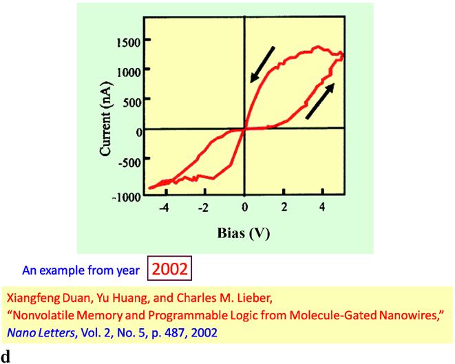
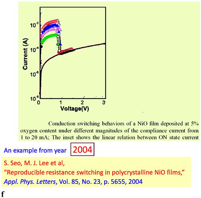
12 776 L. Chua Memristor unfolding example 1 a j = 0, j = 1, 2,...,m b 1 = 1, b k = 0, k= 2, 3,...,n c jk = 0, j = 1, 2,...,p, k= 1, 2,...,r In this case, (43b) reduces to the original memristor equation (29a) (29b). Memristor unfolding example 2 Let us choose the same unfolding parameters as above except b 1 where [ ] RON b 1 = μ v D In this case, (43b) reduces to (6) from [10] describing the famous HP titanium-dioxide memristor reported in a seminal paper in the May issue of Nature [10]. Memristor unfolding example 3 Let us choose a j = 0, j = 1, 2,...,m and c jk = 0, j = 1, 2,...,p, k= 1, 2,...,r In this case, the memristor unfolding assumes the following form: State-dependent Ohm s law: v = R(x)i (44a) State equation: dx/dt = m(i) (44b) By choosing different values for the unfolding parameters b k, the resulting nonlinear scalar function m(i) in (44b) can be used to massage the corresponding pinched hysteresis loop into almost any shape which best approximates the experimental data. In particular, the odd-symmetric pinched hysteresis loops shown in Figs. 1(b), 5(c), and 6(e) can be deformed and morphed into other non-symmetrical shapes, such as the one alluded to [8] in the previous section. We will henceforth call the function m(i) in (44b) the memristor morphing function since it can be chosen to approximate numerous non symmetrical pinched hysteresis loops measured experimentally from real resistance-switching devices, such as those exhibited in Figs. 8(a) 8(k), which were sampled from the literature on non-volatile resistance switching devices. Fig. 8 A sample of 12 experimentally measured pinched hysteresis loops extracted from dozens of similar loops published in the literature on a large variety of resistance switching devices, made from different materials, processes and physical mechanisms


13 Resistance switching memories are memristors 777 Fig. 8 (Continued) Fig. 8 (Continued)

, the memristor state equation is thereby endowed with the following nonvolatility property: dx/dt = f(x,i)= 0, when i = 0 (45b) In other words, (x,i)= (x, 0) is an equilibrium point of the")
14 778 L. Chua such as chaos, which is not considered in this tutorial. Indeed, to build a non-volatile resistance switching memory exhibiting the fine details depicted in some of the pinched hysteresis loops shown in Fig. 8, we only need to consider a subclass of the memristor morphing function f(x,i)in (40b), namely, the class satisfying the condition f(x,i)= 0, whenever i = 0 (45a) Under the constraint imposed by (45a), the memristor state equation is thereby endowed with the following nonvolatility property: dx/dt = f(x,i)= 0, when i = 0 (45b) In other words, (x,i)= (x, 0) is an equilibrium point of the memristor state (40b), for any value of x. Hence, we have a continuum of stable equilibrium points, when i = 0, just as in the case of the ideal memristor of yore. This means that when we switch off the power at t = 0, such that i(t) = 0, for t>0, the state vector x in (42) does not have to tend to zero, but is held unchanged at x(t) = x(0) for all t>0, where x(0) can be set by applying an appropriate input switching signal. But since we can choose many state variables, along with their numerous unfolding parameters, the device engineer has many degrees of freedom to massage his memristor model and optimize a memristance function R(x,i), and a corresponding memristor morphing function f(x,i), to develop a memristor model capable of reproducing almost any fine details observed from their experiments. 7.2 Negative resistance Fig. 8 (Continued) 7.1 Non-volatile memristors A careful examination of the 12 memristor pinched hysteresis loops exhibited in Figs. 8(a) to 8(k) shows that except for Figs. 8(a), 8(d), and 8(h), most of the loops can be reproduced approximately by the preceding simpler memristor (44a) (44b). A few of the pinched hysteresis loops, such as Figs. 8(a), 8(d), 8(i) and 8(j) contains small oscillatory or noisy signal components superimposed upon them. Since the cited authors did not provide details on how their pinched hysteresis loops were measured, we can only conjecture that these small-signal components were either artifacts of their measurement systems, or they may represent genuine nonlinear dynamical phenomena. In the latter case, it may be necessary to use the generic memristor (40a) (40b) to reproduce them. We wish to stress, however, that even this seemingly complex case would represent only the tip of an iceberg of vast nonlinear dynamical phenomena, Let us observe next that the pinched hysteresis loops shown in Fig. 8(h) and Fig. 8(k) contain a non-monotonic currentcontrolled region with a negative slope (i.e., a negative small-signal resistance), implying that the device is locally active [3], and is capable of oscillation under dc bias. Such a pinched hysteresis loop could not be realized by any ideal passive memristor [1], but it can be realized by connecting a locally active current-controlled nonlinear resistor in series with a passive memristor described by (44a), as shown in Fig. 9(a). Note that the resulting one-port in Fig. 9(a) is equivalent to a memristor described by the generic memristor (40a) (40b). To prove this equivalence property, let the memristor be described by v 1 = R(x)i 1 (46a) Let the locally active current-controlled nonlinear resistor be described by v 2 = h(i 2 ) (46b)
15 Resistance switching memories are memristors 779 Fig. 9 The memristor-resistorseriesconnectedcircuitin (a) is equivalent to another memristor with a transformed characteristic. In general, a one-port (2-terminal black box) made of arbitrary interconnections of arbitrary assortments of memristors and resistors is also equivalent to a memristor characterized by a more complex constitutive relation [3] Applying Kirchoff Current Law (KCL), we obtain i = i 1 = i 2 (47) Applying the Kirchoff Voltage Law (KVL), we obtain v = v 1 + v 2 (48) Substituting (46a) (46b) into(48), and making use of (47), we obtain the following equation for the one-port: v = R(x)i + h(i) (49) Since (49) is a special case of (40a), the composite one-port in Fig. 9(a) is a memristor. The above example is but a special case of the following general result. Memristor-resistor interconnection theorem Any one-port made of an arbitrary interconnection of memristors and passive nonlinear resistors, is equivalent to a memristor described by either (40a) (40b), or by an implicit system of equations, whose behavior seen from outside the composite one-port shown in Fig. 9(b) bears all of the fingerprints of a memristor [2]. 7.3 Is memristor negative resistance real or artifact? A careful examination of Figs. 8(a), 8(d), 8(h) and 8(k) reveals that these pinched hysteresis loops contain a small region with a negative slope. Assuming these regions are real measurements pertaining to the device, and not artifacts introduced via the measuring instruments, and/or their inflexible softwares, can we conclude that these devices are endowed with a small-signal (i.e., differential) resistance operating region, and hence is locally active, and can be designed to amplify small signals, and/or to function as an oscillator [3] via an external biasing circuit? The answer is no! Indeed, in many cases, the negative slope is merely a manifestation of a phase-lag between the maxima (or, peak) of the response voltage v(t) (resp., current i(t)) and the peak of its excitation current waveform i(t) (resp., voltage waveform v(t)). This phenomenon is best seen in Figs. 1(b), 1(c), and 1(d) where the voltage peak in Fig. 1(d) lags behind the input current peak in Fig. 1(c). Observe that there is a short time interval where the voltage v(t) in Fig. 1(d) increases while the input current i(t) decreases. This phenomenon occurs after the pinched hysteresis loop in Fig. 1(b) reaches its peak at i = 1, and is the sole mechanism which gives rise to the negative slope. It has nothing to do with local activity [3]! So how can we determine which of the pinched hysteresis loops in Fig. 8 with a negative-slope region is a bona fide small-signal resistance? The generic answer is we do not know unless we have already derived a realistic memristor circuit model, such as Fig. 9, or a memristor state equation, such as (40b), where we can find a point (V, I) on the negative-slope region of the pinched hysteresis loop which can be proved analytically to be an equilibrium point (otherwise known as a dc operating point in electronic circuit jargon), namely, dx/dt = f(x,i)= 0, V = R(x(I), I)I (50 ) for some state variable x = x(i), which depends on I.This means that there exists a dc operating point (V, I) where, in the absence of noise, there is a state variable x = x(i) where the composite memristor-biasing circuit is in equilibrium. This situation is usually not observable experimentally because the memristor small-signal resistance would usually make the circuit unstable, resulting in an oscillation. This alone suffices to conclude that the memristor is locally active. However, for pedagogical reasons, we can design an appropriate external stabilizing biasing circuit such that the composite circuit is locally asymptotically stable [3], whereupon the dc operating point (V, I) on the memristor pinched hysteresis loop can actually be measured. Alternately, we can determine whether the memristor is locally active by deriving first either a memristor circuit model, or a memristor state equation, and then apply standard nonlinear circuit analysis methods to determine whether there exists a locally active equilibrium point [3]. Observe that for an ideal memristor we have x = q, and the equilibrium state equation dq/dt = I = 0 (50 ) does not have a solution if I 0. It follows that an ideal memristor can have only one dc operating point; namely, the origin (v, i) = (V, I) = (0, 0). If the small-signal resistance at the origin is negative, this would imply that the
16 780 L. Chua pinched hysteresis loop has a branch which crosses the origin into the 2nd and the 4th quadrants of the v i plane, implying that the memristor is not passive. It follows therefore that an ideal memristor cannot exhibit a small-signal negative resistance unless it is locally active at the origin, which is possible only if the memristor has an internal source of power, such as light, chemical or nuclear reactions, or batteries, as demonstrated in Fig. 4(f), page 511 of [1], where a locally active memristor exhibiting a negative slope at the origin of the q vs. ϕ curve was built using transistors and op amps (see Fig. 2, p. 509 of [1]), powered by batteries. We can conclude therefore that if the pinched hysteresis loop of a physical device without internal power source exhibits a bona fide small-signal negative resistance, then that device cannot be an ideal memristor, and must therefore be an unfolded memristor sibling, characterized by (40a) (40b). satisfying (53) is endowed with an infinite memory store. In the context of this special issue, we will consider only the special case of binary memory where only two sufficiently distant memory states are of interest because they will be used to store the 0 and 1 states for digital electronics. In this case, the ideal memristor ϕ vs. q curve only needs to have two approximately linear regions, where one region should have as small a slope as possible, while the other region should have as large a slope as possible. The Continuous non-volatility condition (53) guarantees a continuum of tunable resistances, which is essential for synaptive learning applications. Fornon-volatile binary memory applications, we can replace (53) by the following less restrictive condition. Discrete non-volatility condition 8 Switching and sensing resistance memory We have presented in the preceding section a very special subclass, albeit of great interests to the theme of this special issue, of memristors whose members are endowed with the priceless, and timeless, gift of non-volatile memories. This subclass is defined by the memristor constitutive relation v = R(x,i)i (50) dx/dt = f(x,i) (51) where the memristance function R(x,i) satisfies the memristor passivity condition R(x,i) 0 (52) and where the memristor dynamical function f(x,i)satisfies the following condition. Continuous non-volatility condition f(x,i)= 0, if i = 0 (53) The non-volatility condition (53) ensures that any state variable x is a stable, non-isolated, equilibrium point of the memristor state equation (51) when i = 0, or equivalently, when the power is switched off. In other words, (53) isthe genesis of the memristor s memory non-volatility. Observe that since every x is an equilibrium state of (51) when i = 0, the subclass of memristors defined by (53) has a continuum of equilibrium states, where every equilibrium state is stable, but not asymptotically stable [3] in the sense that while small perturbations around each equilibrium state may perturb its location slightly, it will never diverge beyond its perturbed boundary [3]. Hence, in principle, every memristor f(x, 0) = 0 and f(x, 0) = 0 (53 ) where x and x denote two locally asymptotically stable equilibrium points of the memristor state equation (40b) with i = 0, i.e., dx/dt = f(x, 0) (40b ) As an example, consider the state equation: dx/dt = x x 3 i (40b ) Here, x = x = 1 and x = x = 1aretwoisolated locally asymptotically stable equilibrium points of dx(t)/dt = x x 3 (40b ) obtained by setting i = 0in(40b ). Let us now pause to consider some examples. 12 Any device capable of non-volatile memory is useless unless it is relatively easy and inexpensive to sense its memory state. One of the great virtues of the memristor is that since its memristance function in (44a) is a state-dependent resistance obeying Ohm s law, one only needs to inject a small sensing voltage (resp., current), and observe its response. Since in practice, the two resistance memory states R OFF and R ON are chosen so that their ratio is sufficiently large, one can easily determine the memory state by observing the magnitude of the current (resp., voltage) response, to a small ac sensing voltage (resp., current) signal, or a small doubletlike pulse signal with a zero average area. The reason for requiring the sensing signal to have a zero dc average is to prevent the location of a non-isolated memory state from slowly drifting away. 12 The two memory states are chosen sufficiently far apart in practice to enhance robustness and reliability.
17 Resistance switching memories are memristors 781 Memristor switching example 1: bipolar switching Let us revisit the two-state charge-controlled memristor in Fig. 5. To switch from the low-resistance state R 1 corresponding to the middle segment with a small slope to the high-resistance state R 0 corresponding to the upper segment with the much steeper slope, we simply apply a sufficiently large current pulse so that its corresponding charge q(t) would traverse beyond the charge breakpoint q = B. To switch back from a point on the upper segment (highresistance state R 0, simply apply a similar pulse of the opposite polarity. This method of switching is usually referred to as bipolar resistance switching. Our next example illustrates how switching can be achieved by applying switching pulses of the same polarity, but of different amplitudes, often referred to in practice as unipolar resistance switching. Memristor switching example 2: unipolar switching Consider the flux-controlled memristor depicted in Fig. 10 with a 7-segment piecewise-linear ϕ q curve (Fig. 10(a)). Here the three parallel red segments with a steep slope have a high conductance state G ON, whereas the four parallel green segments with a much smaller slope have a much smaller conductance state G OFF. For the memristor constitutive relation shown in Fig. 10(a), we can switch from a high conductance state to a low-conductance state with a relatively small-amplitude voltage pulse since it only needs a small increment ϕ in ϕ to cross the breakpoint B 1 into the low-conductance state. In contrast, a much larger amplitude voltage pulse, but of the same polarity, and the same pulse width, would be needed in order to reach the next breakpoint B 2, and beyond, in order to switch back to a high conductance state G ON again. The same switching sequence with the opposite polarity can also be executed to achieve the same results, as illustrated in Fig. 10(b). The corresponding switching loci plotted in the v i plane is shown in Fig. 10(c). Here, to prevent the excessive current jump from a small current to a very high current, thereby damaging the device, measuring instruments are normally programmed to clamp the current at a maximum safe value, called the compliance current level in industry, as illustrated in Fig. 10(c). The above mode of using voltage pulses of the same polarity to switch between low- and high-resistance states has been reported in some so-called unipolar devices in industry [11]. 9 Concluding remarks Any electronic device with only two electrical terminals is usually referred to in the semiconductor industry as a nonvolatile resistance-switching memory device if the device can exhibit one of two resistance values over a sufficiently Fig. 10 A staircase-like flux-controlled memristor can switch from a high conductance to a low-conductance state using voltage pulses of the same polarity, somewhat reminiscent of the unipolar switching characteristic depicted in Fig. 1(a) of [7] long time period, without consuming any power, and can be switched from a low-resistance state to a high-resistance state, and vice versa, by applying either a short voltage pulse, or a short current pulse, of appropriate amplitude and polarity, across the two device terminals, and such that the resistance state at any time, either low or high, can be sensed by applying a relatively much smaller sensing voltage pulse, or current pulse, of some preset waveform, across the same terminals. Implicit in the above definition is that at any time, the device can be modeled as a linear resistor obeying Ohm s Law, when the sensing signal amplitude is sufficiently small, for otherwise, the word resistance would be meaningless. The linearity property implies that the sensing voltage, or current, and its corresponding voltage response, or current response, have identical waveforms, and have the same zerocrossings in time. It follows that the loci in the v i plane during sensing when observed from an oscilloscope will appear as a short linear segment through the origin whose slope will be small if the resistance being sensed is low, or much larger, if the resistance being sensed is high. In other words, the two resistance states can be depicted as two short straight line segments of slopes R 1 and R 2, crossing each other at the origin of the v i plane. These two segments can be emu-

18 782 L. Chua lated exactly by an ideal memristor having the memristance R(q) = R 1 at the origin, and R(q) = R 2 at another point, say q = q 2 of a smooth ϕ vs. q curve in the ϕ vs. q plane. By uncovering the physical operating mechanisms taking place internal to the device, one could construct a model that not only exhibits these two memristances, but also faithfully reproduces one or more pinched hysteresis loops, measured using different large-amplitude periodic signals [12]. The resulting mathematical expressions may be extremely complex, and may often be expressible only by implicit mathematical equations. Nevertheless, they would define a memristor of the generic form given by (40a) (40b), by virtue of the characteristic property of the memristor. The take-home lesson from this tutorial can be summarized succinctly as follow: Any 2-terminal electronic device devoid of internal power source and which is capable of switching between two resistances upon application of an appropriate voltage or current signal, and whose resistance state at any instant of time can be sensed by applying a relatively much smaller sensing signal, is a memristor, defined either by the ideal memristor equation, or by one of its unfolded siblings via (40a) (40b). Our final remark is concerned with the significance of the pinched hysteresis loop in the modeling of non-volatile resistance switching memories. Let us recall that while the memristance vs. state map tells us the complete set of smallsignal memristances endowed upon a memristive device, it is rather difficult to measure them experimentally unless the memristor can be modeled by the ideal memristor equation v = R(q)i, where dq/dt = i. To extract such information from the generic memristor (40a) (40b), we have to identify first the relevant state variable, or state variables in cases demanding a higher-order memristor state space. In contrast, the chord memristances associated with a pinched hysteresis loop can be readily extracted since it is simply the set of all slopes of a straight line anchored at the origin whose tips traces along the loci of a measured pinched hysteresis loop. Each such chord resistance is a true resistance indistinguishable from a linear resistor having the same resistance. The set of all such chord memristances associated with a pinched hysteresis loop therefore provides a subset of the memristor s endowed small-signal memristances. Since measuring pinched hysteresis loops associated with different periodic input voltage, or current, waveforms applied across a memristive device is a relatively simple task that could be automated, 13 it is a useful tool for uncovering a memristive device s nonlinear physical operating mechanisms, and for validating its memristive models. In the case 13 Measurement instrument companies could exploit the high market potentials of automated pinched-hysteresis-loop measuring instrumentations, and their memristance extractions. Fig. 11 An enlargement of the first 25 axiomatically defined circuit elements from the periodic table of circuit elements (Fig. 31 of [3]) where the four basic circuit elements (resistor, capacitor, inductors and memristor) are replaced by their symbols. The memcapacitor is located at (a, b) = ( 1, 2) and the meminductor is located at (a, b) = ( 2, 1). Observe that since these two elements require double time integrals of voltage and current, their dynamics are of a higher order than those of the four basic circuit elements enclosed inside the dotted red box of an ideal memristor, it is important to bear in mind that the small-signal memristance, and its corresponding chord memristance, represent exactly the same information. The main difference is that while the chord memristance is a long vector pinned at the origin of the v i plane, its corresponding small-signal memristance is an infinitesimal tangent attached at each point on an ideal memristor s constitutive relation in the ϕ vs. q plane. It is also useful to note that unlike classical electronic circuit analysis, the small-signal memristor voltage associated with an applied small-signal memristor current represents the actual total solution, and is not superimposed upon some dc bias. We end this tutorial with the following terse characterization of a resistance switching memory device: 14 If it s pinched, it s a memristor. Acknowledgements This research is supported in part by a Guggenheim Fellowship, The Leverhulme Trust Visiting Professorship, and an 14 Exactly the same theory of the memristor can be used to identify a memcapacitor (acronym for memory capacitor), and a meminductor (acronym for a memory inductor), from the table of axiomaticallydefined circuit elements [3] and[4], as depicted in Fig. 11, and presented at the 2008 Berkeley Symposium on Memristors and Memristive Systems (Part 1, towards the end of the opening lecture) on Nov. 21, 2008 (proceedings of this symposium were videotaped and available via YouTube), as well as further elucidated in [13] and[14].
Electric Current. Note: Current has polarity. EECS 42, Spring 2005 Week 2a 1
 Electric Current Definition: rate of positive charge flow Symbol: i Units: Coulombs per second Amperes (A) i = dq/dt where q = charge (in Coulombs), t = time (in seconds) Note: Current has polarity. EECS
Implementing Memristor Based Chaotic Circuits
 Implementing Memristor Based Chaotic Circuits Bharathwaj Muthuswamy Electrical Engineering and Computer Sciences University of California at Berkeley Technical Report No. UCB/EECS-2009-156 http://www.eecs.berkeley.edu/pubs/techrpts/2009/eecs-2009-156.html
Energy Storage Elements: Capacitors and Inductors
 CHAPTER 6 Energy Storage Elements: Capacitors and Inductors To this point in our study of electronic circuits, time has not been important. The analysis and designs we have performed so far have been static,
Lecture #3. Review: Power
 Lecture #3 OUTLINE Power calculations Circuit elements Voltage and current sources Electrical resistance (Ohm s law) Kirchhoff s laws Reading Chapter 2 Lecture 3, Slide 1 Review: Power If an element is
ECE2262 Electric Circuits. Chapter 6: Capacitance and Inductance
 ECE2262 Electric Circuits Chapter 6: Capacitance and Inductance Capacitors Inductors Capacitor and Inductor Combinations Op-Amp Integrator and Op-Amp Differentiator 1 CAPACITANCE AND INDUCTANCE Introduces
Figure 1.1: Schematic symbols of an N-transistor and P-transistor
 Chapter 1 The digital abstraction The term a digital circuit refers to a device that works in a binary world. In the binary world, the only values are zeros and ones. Hence, the inputs of a digital circuit
Pinched hysteresis loops are a fingerprint of square law capacitors
 Pinched hysteresis loops are a fingerprint of square law capacitors Blaise Mouttet Abstract It has been claimed that pinched hysteresis curves are the fingerprint of memristors. This paper demonstrates
A short history of memristor development. R. Stanley Williams HP Labs
 A short history of memristor development R. Stanley Williams HP Labs Historical Background During the 1960's, Prof. Leon Chua, who was then at Purdue University, established the mathematical foundation
Chapter 1 The Electric Force
 Chapter 1 The Electric Force 1. Properties of the Electric Charges 1- There are two kinds of the electric charges in the nature, which are positive and negative charges. - The charges of opposite sign
REUNotes08-CircuitBasics May 28, 2008
 Chapter One Circuits (... introduction here... ) 1.1 CIRCUIT BASICS Objects may possess a property known as electric charge. By convention, an electron has one negative charge ( 1) and a proton has one
Electromagnetic Induction (Chapters 31-32)
") Electromagnetic Induction (Chapters 31-3) The laws of emf induction: Faraday s and Lenz s laws Inductance Mutual inductance M Self inductance L. Inductors Magnetic field energy Simple inductive circuits
Electromagnetic Induction (Chapters 31-3) The laws of emf induction: Faraday s and Lenz s laws Inductance Mutual inductance M Self inductance L. Inductors Magnetic field energy Simple inductive circuits
ELECTRONICS. EE 42/100 Lecture 2: Charge, Current, Voltage, and Circuits. Revised 1/18/2012 (9:04PM) Prof. Ali M. Niknejad
 Prof. Ali M. Niknejad") A. M. Niknejad University of California, Berkeley EE 100 / 42 Lecture 2 p. 1/26 EE 42/100 Lecture 2: Charge, Current, Voltage, and Circuits ELECTRONICS Revised 1/18/2012 (9:04PM) Prof. Ali M. Niknejad
A. M. Niknejad University of California, Berkeley EE 100 / 42 Lecture 2 p. 1/26 EE 42/100 Lecture 2: Charge, Current, Voltage, and Circuits ELECTRONICS Revised 1/18/2012 (9:04PM) Prof. Ali M. Niknejad
Electrical Eng. fundamental Lecture 1
 Electrical Eng. fundamental Lecture 1 Contact details: h-elhelw@staffs.ac.uk Introduction Electrical systems pervade our lives; they are found in home, school, workplaces, factories,
AC&ST AUTOMATIC CONTROL AND SYSTEM THEORY SYSTEMS AND MODELS. Claudio Melchiorri
 C. Melchiorri (DEI) Automatic Control & System Theory 1 AUTOMATIC CONTROL AND SYSTEM THEORY SYSTEMS AND MODELS Claudio Melchiorri Dipartimento di Ingegneria dell Energia Elettrica e dell Informazione (DEI)
Physics 142 Steady Currents Page 1. Steady Currents
 Physics 142 Steady Currents Page 1 Steady Currents If at first you don t succeed, try, try again. Then quit. No sense being a damn fool about it. W.C. Fields Electric current: the slow average drift of
ELECTRICAL THEORY. Ideal Basic Circuit Element
 ELECTRICAL THEORY PROF. SIRIPONG POTISUK ELEC 106 Ideal Basic Circuit Element Has only two terminals which are points of connection to other circuit components Can be described mathematically in terms
Divergent Fields, Charge, and Capacitance in FDTD Simulations
 Divergent Fields, Charge, and Capacitance in FDTD Simulations Christopher L. Wagner and John B. Schneider August 2, 1998 Abstract Finite-difference time-domain (FDTD) grids are often described as being
Notes for course EE1.1 Circuit Analysis TOPIC 10 2-PORT CIRCUITS
 Objectives: Introduction Notes for course EE1.1 Circuit Analysis 4-5 Re-examination of 1-port sub-circuits Admittance parameters for -port circuits TOPIC 1 -PORT CIRCUITS Gain and port impedance from -port
Designing Information Devices and Systems I Fall 2018 Lecture Notes Note Introduction: Op-amps in Negative Feedback
 EECS 16A Designing Information Devices and Systems I Fall 2018 Lecture Notes Note 18 18.1 Introduction: Op-amps in Negative Feedback In the last note, we saw that can use an op-amp as a comparator. However,
12 Chapter Driven RLC Circuits
 hapter Driven ircuits. A Sources... -. A ircuits with a Source and One ircuit Element... -3.. Purely esistive oad... -3.. Purely Inductive oad... -6..3 Purely apacitive oad... -8.3 The Series ircuit...
RC, RL, and LCR Circuits
 RC, RL, and LCR Circuits EK307 Lab Note: This is a two week lab. Most students complete part A in week one and part B in week two. Introduction: Inductors and capacitors are energy storage devices. They
Alternating Current. Symbol for A.C. source. A.C.
 Alternating Current Kirchoff s rules for loops and junctions may be used to analyze complicated circuits such as the one below, powered by an alternating current (A.C.) source. But the analysis can quickly
Physics 212 Midterm 2 Form A
 1. A wire contains a steady current of 2 A. The charge that passes a cross section in 2 s is: A. 3.2 10-19 C B. 6.4 10-19 C C. 1 C D. 2 C E. 4 C 2. In a Physics 212 lab, Jane measures the current versus
Frequency Dependent Aspects of Op-amps
 Frequency Dependent Aspects of Op-amps Frequency dependent feedback circuits The arguments that lead to expressions describing the circuit gain of inverting and non-inverting amplifier circuits with resistive
Chapter 7. Electrodynamics
 Chapter 7. Electrodynamics Summary: Electrostatics and Magnetostatics E / B E B J P E M 1 mb e D E P H B/ M D H f J f E V B A b P Pn b Jb M K M n b D E B H (1 ) (1 ) e m 7.1 Electromotive Force 7.1.1 Ohm
Current and Resistance
 Chapter 26 Current and Resistance Copyright 26-1 Electric Current As Fig. (a) reminds us, any isolated conducting loop regardless of whether it has an excess charge is all at the same potential. No electric
Electric Currents. Resistors (Chapters 27-28)
") Electric Currents. Resistors (Chapters 27-28) Electric current I Resistance R and resistors Relation between current and resistance: Ohm s Law Resistivity ρ Energy dissipated by current. Electric power
Electric Currents. Resistors (Chapters 27-28) Electric current I Resistance R and resistors Relation between current and resistance: Ohm s Law Resistivity ρ Energy dissipated by current. Electric power
Chapter 2. Engr228 Circuit Analysis. Dr Curtis Nelson
 Chapter 2 Engr228 Circuit Analysis Dr Curtis Nelson Chapter 2 Objectives Understand symbols and behavior of the following circuit elements: Independent voltage and current sources; Dependent voltage and
AC vs. DC Circuits. Constant voltage circuits. The voltage from an outlet is alternating voltage
 Circuits AC vs. DC Circuits Constant voltage circuits Typically referred to as direct current or DC Computers, logic circuits, and battery operated devices are examples of DC circuits The voltage from
Sinusoids and Phasors
 CHAPTER 9 Sinusoids and Phasors We now begins the analysis of circuits in which the voltage or current sources are time-varying. In this chapter, we are particularly interested in sinusoidally time-varying
ENGG 225. David Ng. Winter January 9, Circuits, Currents, and Voltages... 5
 ENGG 225 David Ng Winter 2017 Contents 1 January 9, 2017 5 1.1 Circuits, Currents, and Voltages.................... 5 2 January 11, 2017 6 2.1 Ideal Basic Circuit Elements....................... 6 3 January
Parasitic Effects on Memristor Dynamics
 International Journal of Bifurcation and Chaos, Vol. 26, No. 6 (2016) 160014 (55 pages) c World Scientific Publishing Company DOI: 10.1142/S021812741600147 Makoto Itoh 1-19-20-20, Arae, Jonan-ku, Fukuoka
(Refer Slide Time: 01:30)
") Networks and Systems Prof V.G K.Murti Department of Electrical Engineering Indian Institute of Technology, Madras Lecture - 11 Fourier Series (5) Continuing our discussion of Fourier series today, we will
Networks and Systems Prof V.G K.Murti Department of Electrical Engineering Indian Institute of Technology, Madras Lecture - 11 Fourier Series (5) Continuing our discussion of Fourier series today, we will
Basic Laws. Bởi: Sy Hien Dinh
 Basic Laws Bởi: Sy Hien Dinh INTRODUCTION Chapter 1 introduced basic concepts such as current, voltage, and power in an electric circuit. To actually determine the values of this variable in a given circuit
CHAPTER D.C. CIRCUITS
 Solutions--Ch. 16 (D.C. Circuits) CHAPTER 16 -- D.C. CIRCUITS 16.1) Consider the circuit to the right: a.) The voltage drop across R must be zero if there is to be no current through it, which means the
Circuit Theory Prof. S.C. Dutta Roy Department of Electrical Engineering Indian Institute of Technology, Delhi
 Circuit Theory Prof. S.C. Dutta Roy Department of Electrical Engineering Indian Institute of Technology, Delhi Lecture - 1 Review of Signals and Systems Welcome to this course E E 202 circuit theory 4
ENGR 2405 Class No Electric Circuits I
 ENGR 2405 Class No. 48056 Electric Circuits I Dr. R. Williams Ph.D. rube.williams@hccs.edu Electric Circuit An electric circuit is an interconnec9on of electrical elements Charge Charge is an electrical
Physics 4 Spring 1989 Lab 5 - AC Circuits
 Physics 4 Spring 1989 Lab 5 - AC Circuits Theory Consider the series inductor-resistor-capacitor circuit shown in figure 1. When an alternating voltage is applied to this circuit, the current and voltage
ELECTRIC CURRENT. Ions CHAPTER Electrons. ELECTRIC CURRENT and DIRECT-CURRENT CIRCUITS
 LCTRC CURRNT CHAPTR 25 LCTRC CURRNT and DRCTCURRNT CRCUTS Current as the motion of charges The Ampère Resistance and Ohm s Law Ohmic and nonohmic materials lectrical energy and power ons lectrons nside
Some of the different forms of a signal, obtained by transformations, are shown in the figure. jwt e z. jwt z e
 Transform methods Some of the different forms of a signal, obtained by transformations, are shown in the figure. X(s) X(t) L - L F - F jw s s jw X(jw) X*(t) F - F X*(jw) jwt e z jwt z e X(nT) Z - Z X(z)
What happens when things change. Transient current and voltage relationships in a simple resistive circuit.
 Module 4 AC Theory What happens when things change. What you'll learn in Module 4. 4.1 Resistors in DC Circuits Transient events in DC circuits. The difference between Ideal and Practical circuits Transient
EXPERIMENT 12 OHM S LAW
 EXPERIMENT 12 OHM S LAW INTRODUCTION: We will study electricity as a flow of electric charge, sometimes making analogies to the flow of water through a pipe. In order for electric charge to flow a complete
ECE2262 Electric Circuits. Chapter 6: Capacitance and Inductance
 ECE2262 Electric Circuits Chapter 6: Capacitance and Inductance Capacitors Inductors Capacitor and Inductor Combinations 1 CAPACITANCE AND INDUCTANCE Introduces two passive, energy storing devices: Capacitors
EE 330 Lecture 22. Small Signal Modelling Operating Points for Amplifier Applications Amplification with Transistor Circuits
 EE 330 Lecture 22 Small Signal Modelling Operating Points for Amplifier Applications Amplification with Transistor Circuits Exam 2 Friday March 9 Exam 3 Friday April 13 Review Session for Exam 2: 6:00
ES250: Electrical Science. HW1: Electric Circuit Variables, Elements and Kirchhoff s Laws
 ES250: Electrical Science HW1: Electric Circuit Variables, Elements and Kirchhoff s Laws Introduction Engineers use electric circuits to solve problems that are important to modern society, such as: 1.
Basic Electronics. Introductory Lecture Course for. Technology and Instrumentation in Particle Physics Chicago, Illinois June 9-14, 2011
 Basic Electronics Introductory Lecture Course for Technology and Instrumentation in Particle Physics 2011 Chicago, Illinois June 9-14, 2011 Presented By Gary Drake Argonne National Laboratory drake@anl.gov
Direct-Current Circuits. Physics 231 Lecture 6-1
 Direct-Current Circuits Physics 231 Lecture 6-1 esistors in Series and Parallel As with capacitors, resistors are often in series and parallel configurations in circuits Series Parallel The question then
Designing Information Devices and Systems I Spring 2015 Note 11
 EECS 16A Designing Information Devices and Systems I Spring 2015 Note 11 Lecture notes by Edward Wang (02/26/2015). Resistors Review Ohm s law: V = IR Water pipe circuit analogy: Figure 1: Water analogy
8. Electric Currents
 8. Electric Currents S. G. Rajeev January 30, 2011 An electric current is produced by the movement of electric charges. In most cases these are electrons. A conductor is a material through which an electric
Electric Current. Chapter 17. Electric Current, cont QUICK QUIZ Current and Resistance. Sections: 1, 3, 4, 6, 7, 9
 Electric Current Chapter 17 Current and Resistance Sections: 1, 3, 4, 6, 7, 9 Whenever electric charges of like signs move, an electric current is said to exist The current is the rate at which the charge
01 Harmonic Oscillations
 Utah State University DigitalCommons@USU Foundations of Wave Phenomena Library Digital Monographs 8-2014 01 Harmonic Oscillations Charles G. Torre Department of Physics, Utah State University, Charles.Torre@usu.edu
Appendix A Installing QUCS
 Appendix A Installing QUCS In this appendix, we will discuss how to install QUCS [1]. Note that QUCS has a lot of components, many of which we will not use. Nevertheless, we will install all components
Chapter 28 Solutions
 Chapter 8 Solutions 8.1 (a) P ( V) R becomes 0.0 W (11.6 V) R so R 6.73 Ω (b) V IR so 11.6 V I (6.73 Ω) and I 1.7 A ε IR + Ir so 15.0 V 11.6 V + (1.7 A)r r 1.97 Ω Figure for Goal Solution Goal Solution
Window Function Analysis of Nonlinear Behaviour of Fourth Fundamental Passive Circuit Element: Memristor
 IOSR Journal of Electronics and Communication Engineering (IOSR-JECE) e-issn: 2278-2834,p- ISSN: 2278-8735.Volume 12, Issue 3, Ver. III (May - June 217), PP 58-63 www.iosrjournals.org Window Function Analysis
MTH301 Calculus II Glossary For Final Term Exam Preparation
 MTH301 Calculus II Glossary For Final Term Exam Preparation Glossary Absolute maximum : The output value of the highest point on a graph over a given input interval or over all possible input values. An
a + b Time Domain i(τ)dτ.
dτ.") R, C, and L Elements and their v and i relationships We deal with three essential elements in circuit analysis: Resistance R Capacitance C Inductance L Their v and i relationships are summarized below.
R, C, and L Elements and their v and i relationships We deal with three essential elements in circuit analysis: Resistance R Capacitance C Inductance L Their v and i relationships are summarized below.
Look over Chapter 26 sections 1-7 Examples 3, 7. Look over Chapter 18 sections 1-5, 8 over examples 1, 2, 5, 8, 9,
 Look over Chapter 26 sections 1-7 Examples 3, 7 Look over Chapter 18 sections 1-5, 8 over examples 1, 2, 5, 8, 9, 1)How to find a current in a wire. 2)What the Current Density and Draft Speed are. 3)What
Unit 2: Modeling in the Frequency Domain. Unit 2, Part 4: Modeling Electrical Systems. First Example: Via DE. Resistors, Inductors, and Capacitors
 Unit 2: Modeling in the Frequency Domain Part 4: Modeling Electrical Systems Engineering 582: Control Systems I Faculty of Engineering & Applied Science Memorial University of Newfoundland January 20,
Driven RLC Circuits Challenge Problem Solutions
 Driven LC Circuits Challenge Problem Solutions Problem : Using the same circuit as in problem 6, only this time leaving the function generator on and driving below resonance, which in the following pairs
KIRCHHOFF S LAWS. Learn how to analyze more complicated circuits with more than one voltage source and numerous resistors.
 KIRCHHOFF S LAWS Lab Goals: Learn how to analyze more complicated circuits with more than one voltage source and numerous resistors. Lab Notebooks: Write descriptions of all of your experiments in your
Modeling of Electromechanical Systems
 Page 1 of 54 Modeling of Electromechanical Systems Werner Haas, Kurt Schlacher and Reinhard Gahleitner Johannes Kepler University Linz, Department of Automatic Control, Altenbergerstr.69, A 4040 Linz,
Nonlinear Autonomous Systems of Differential
 Chapter 4 Nonlinear Autonomous Systems of Differential Equations 4.0 The Phase Plane: Linear Systems 4.0.1 Introduction Consider a system of the form x = A(x), (4.0.1) where A is independent of t. Such
Physics 142 AC Circuits Page 1. AC Circuits. I ve had a perfectly lovely evening but this wasn t it. Groucho Marx
 Physics 142 A ircuits Page 1 A ircuits I ve had a perfectly lovely evening but this wasn t it. Groucho Marx Alternating current: generators and values It is relatively easy to devise a source (a generator
Chapter 2 Direct Current Circuits
 Chapter 2 Direct Current Circuits 2.1 Introduction Nowadays, our lives are increasingly dependent upon the availability of devices that make extensive use of electric circuits. The knowledge of the electrical
MATH 162. Midterm 2 ANSWERS November 18, 2005
 MATH 62 Midterm 2 ANSWERS November 8, 2005. (0 points) Does the following integral converge or diverge? To get full credit, you must justify your answer. 3x 2 x 3 + 4x 2 + 2x + 4 dx You may not be able
Magnetized Material (contd.) and Electromagnetic Induction
 and Electromagnetic Induction") Magnetized Material (contd.) and Electromagnetic Induction Lecture 28: Electromagnetic Theory Professor D. K. Ghosh, Physics Department, I.I.T., Bombay In the first half of this lecture we will continue
Magnetized Material (contd.) and Electromagnetic Induction Lecture 28: Electromagnetic Theory Professor D. K. Ghosh, Physics Department, I.I.T., Bombay In the first half of this lecture we will continue
= e = e 3 = = 4.98%
 PHYS 212 Exam 2 - Practice Test - Solutions 1E In order to use the equation for discharging, we should consider the amount of charge remaining after three time constants, which would have to be q(t)/q0.
Experiment 5: Measurements Magnetic Fields
 Experiment 5: Measurements Magnetic Fields Introduction In this laboratory you will use fundamental electromagnetic Equations and principles to measure the magnetic fields of two magnets. 1 Physics 1.1
Chapter 17. Current and Resistance. Sections: 1, 3, 4, 6, 7, 9
 Chapter 17 Current and Resistance Sections: 1, 3, 4, 6, 7, 9 Equations: 2 2 1 e r q q F = k 2 e o r Q k q F E = = I R V = A L R ρ = )] ( 1 [ o o T T + = α ρ ρ V I V t Q P = = R V R I P 2 2 ) ( = = C Q
Chapter 7 Direct-Current Circuits
 Chapter 7 Direct-Current Circuits 7. Introduction... 7. Electromotive Force... 7.3 Resistors in Series and in Parallel... 4 7.4 Kirchhoff s Circuit Rules... 6 7.5 Voltage-Current Measurements... 8 7.6
ECE 2100 Circuit Analysis
 ECE 2100 Circuit Analysis Lesson 3 Chapter 2 Ohm s Law Network Topology: nodes, branches, and loops Daniel M. Litynski, Ph.D. http://homepages.wmich.edu/~dlitynsk/ esistance ESISTANCE = Physical property
Basic Electricity. Unit 2 Basic Instrumentation
 Basic Electricity Unit 2 Basic Instrumentation Outlines Terms related to basic electricity-definitions of EMF, Current, Potential Difference, Power, Energy and Efficiency Definition: Resistance, resistivity
Capacitors. Chapter How capacitors work Inside a capacitor
 Chapter 6 Capacitors In every device we have studied so far sources, resistors, diodes and transistors the relationship between voltage and current depends only on the present, independent of the past.
Networks and Systems Prof V.G K. Murti Department of Electrical Engineering Indian Institute of Technology, Madras Lecture - 10 Fourier Series (10)
") Networks and Systems Prof V.G K. Murti Department of Electrical Engineering Indian Institute of Technology, Madras Lecture - 10 Fourier Series (10) What we have seen in the previous lectures, is first
Networks and Systems Prof V.G K. Murti Department of Electrical Engineering Indian Institute of Technology, Madras Lecture - 10 Fourier Series (10) What we have seen in the previous lectures, is first
Chapter 26 Direct-Current Circuits
 Chapter 26 Direct-Current Circuits 1 Resistors in Series and Parallel In this chapter we introduce the reduction of resistor networks into an equivalent resistor R eq. We also develop a method for analyzing
Complex Dynamics of a Memristor Based Chua s Canonical Circuit
 Complex Dynamics of a Memristor Based Chua s Canonical Circuit CHRISTOS K. VOLOS Department of Mathematics and Engineering Sciences Univ. of Military Education - Hellenic Army Academy Athens, GR6673 GREECE
18 - ELECTROMAGNETIC INDUCTION AND ALTERNATING CURRENTS ( Answers at the end of all questions ) Page 1
 Page 1") ( Answers at the end of all questions ) Page ) The self inductance of the motor of an electric fan is 0 H. In order to impart maximum power at 50 Hz, it should be connected to a capacitance of 8 µ F (
( Answers at the end of all questions ) Page ) The self inductance of the motor of an electric fan is 0 H. In order to impart maximum power at 50 Hz, it should be connected to a capacitance of 8 µ F (
fehmibardak.cbu.tr Temporary Office 348, Mühendislik Fakültesi B Blok
 fehmibardak.cbu.tr Temporary Office 348, Mühendislik Fakültesi B Blok 1 Course Progress Introductory level Electrostatic, Coulomb s Law Electric Field, Gauss Law Magnetic field, Maxwell s Equations Current,
Construction of Classes of Circuit-Independent Chaotic Oscillators Using Passive-Only Nonlinear Devices
 IEEE TRANSACTIONS ON CIRCUITS AND SYSTEMS I: FUNDAMENTAL THEORY AND APPLICATIONS, VOL. 48, NO. 3, MARCH 2001 289 Construction of Classes of Circuit-Independent Chaotic Oscillators Using Passive-Only Nonlinear
Torsion Spring Oscillator with Dry Friction
 Torsion Spring Oscillator with Dry Friction Manual Eugene Butikov Annotation. The manual includes a description of the simulated physical system and a summary of the relevant theoretical material for students
Lecture 05 Power in AC circuit
 CA2627 Building Science Lecture 05 Power in AC circuit Instructor: Jiayu Chen Ph.D. Announcement 1. Makeup Midterm 2. Midterm grade Grade 25 20 15 10 5 0 10 15 20 25 30 35 40 Grade Jiayu Chen, Ph.D. 2
Calculus Relationships in AP Physics C: Electricity and Magnetism
 C: Electricity This chapter focuses on some of the quantitative skills that are important in your C: Mechanics course. These are not all of the skills that you will learn, practice, and apply during the
A Memristor Model with Piecewise Window Function
 RAIOENGINEERING, VOL. 22, NO. 4, ECEMBER 23 969 A Memristor Model with Piecewise Window Function Juntang YU, Xiaomu MU, Xiangming XI, Shuning WANG ept. of Automation, TNList, Tsinghua University, Qinghuayuan,
E40M Review - Part 1
 E40M Review Part 1 Topics in Part 1 (Today): KCL, KVL, Power Devices: V and I sources, R Nodal Analysis. Superposition Devices: Diodes, C, L Time Domain Diode, C, L Circuits Topics in Part 2 (Wed): MOSFETs,
Chapter 4. Techniques of Circuit Analysis
 Chapter 4. Techniques of Circuit Analysis By: FARHAD FARADJI, Ph.D. Assistant Professor, Electrical Engineering, K.N. Toosi University of Technology http://wp.kntu.ac.ir/faradji/electriccircuits1.htm Reference:
ECE 1311: Electric Circuits. Chapter 2: Basic laws
 ECE 1311: Electric Circuits Chapter 2: Basic laws Basic Law Overview Ideal sources series and parallel Ohm s law Definitions open circuits, short circuits, conductance, nodes, branches, loops Kirchhoff's
AN ELECTRIC circuit containing a switch controlled by
 878 IEEE TRANSACTIONS ON CIRCUITS AND SYSTEMS II: ANALOG AND DIGITAL SIGNAL PROCESSING, VOL. 46, NO. 7, JULY 1999 Bifurcation of Switched Nonlinear Dynamical Systems Takuji Kousaka, Member, IEEE, Tetsushi
ME 132, Dynamic Systems and Feedback. Class Notes. Spring Instructor: Prof. A Packard
 ME 132, Dynamic Systems and Feedback Class Notes by Andrew Packard, Kameshwar Poolla & Roberto Horowitz Spring 2005 Instructor: Prof. A Packard Department of Mechanical Engineering University of California
Basic. Theory. ircuit. Charles A. Desoer. Ernest S. Kuh. and. McGraw-Hill Book Company
 Basic C m ш ircuit Theory Charles A. Desoer and Ernest S. Kuh Department of Electrical Engineering and Computer Sciences University of California, Berkeley McGraw-Hill Book Company New York St. Louis San
Chapter 10 Instructor Notes
 G. izzoni, Principles and Applications of lectrical ngineering Problem solutions, hapter 10 hapter 10 nstructor Notes hapter 10 introduces bipolar junction transistors. The material on transistors has
CS 436 HCI Technology Basic Electricity/Electronics Review
 CS 436 HCI Technology Basic Electricity/Electronics Review *Copyright 1997-2008, Perry R. Cook, Princeton University August 27, 2008 1 Basic Quantities and Units 1.1 Charge Number of electrons or units
A simple electronic circuit to demonstrate bifurcation and chaos
 A simple electronic circuit to demonstrate bifurcation and chaos P R Hobson and A N Lansbury Brunel University, Middlesex Chaos has generated much interest recently, and many of the important features
Electric Force and Charge. Electric Force and Charge. Electric Force and Charge. Electric Force and Charge. Electric Force and Charge
 Hewitt/Lyons/Suchocki/Yeh Conceptual Integrated Science Chapter 7 ELECTRICITY AND MAGNETISM Electric forces can attract some objects and repel others Electric charge: the fundamental quantity that underlies
DOWNLOAD PDF AC CIRCUIT ANALYSIS PROBLEMS AND SOLUTIONS
 Chapter 1 : Resistors in Circuits - Practice â The Physics Hypertextbook In AC circuit analysis, if the circuit has sources operating at different frequencies, Superposition theorem can be used to solve
Louisiana State University Physics 2102, Exam 3 April 2nd, 2009.
 PRINT Your Name: Instructor: Louisiana State University Physics 2102, Exam 3 April 2nd, 2009. Please be sure to PRINT your name and class instructor above. The test consists of 4 questions (multiple choice),
Writing Circuit Equations
 2 C H A P T E R Writing Circuit Equations Objectives By the end of this chapter, you should be able to do the following: 1. Find the complete solution of a circuit using the exhaustive, node, and mesh
Chapter 27. Current And Resistance
 Chapter 27 Current And Resistance Electric Current Electric current is the rate of flow of charge through some region of space The SI unit of current is the ampere (A) 1 A = 1 C / s The symbol for electric
Discussion Question 7A P212, Week 7 RC Circuits
 Discussion Question 7A P1, Week 7 RC Circuits The circuit shown initially has the acitor uncharged, and the switch connected to neither terminal. At time t = 0, the switch is thrown to position a. C a
Response of Second-Order Systems
 Unit 3 Response of SecondOrder Systems In this unit, we consider the natural and step responses of simple series and parallel circuits containing inductors, capacitors and resistors. The equations which
PHYS 212 Final Exam (Old Material) Solutions - Practice Test
 Solutions - Practice Test") PHYS 212 Final Exam (Old Material) Solutions - Practice Test 1E If the ball is attracted to the rod, it must be made of a conductive material, otherwise it would not have been influenced by the nearby
PHYS 212 Final Exam (Old Material) Solutions - Practice Test 1E If the ball is attracted to the rod, it must be made of a conductive material, otherwise it would not have been influenced by the nearby