Nanoscale tunable reduction of graphene oxide for graphene electronics
|
|
|
- Tabitha Hawkins
- 6 years ago
- Views:
Transcription


1 Nanoscale tunable reduction of graphene oxide for graphene electronics Z. Wei, D. Wang, Suenne Kim, S. Y. Kim, Yike Hu, M. K. Yakes, A.R. Laracuente, Z. Dai, S.R. Marder, Claire Berger, et al. To cite this version: Z. Wei, D. Wang, Suenne Kim, S. Y. Kim, Yike Hu, et al.. Nanoscale tunable reduction of graphene oxide for graphene electronics. Science, American Association for the Advancement of Science, 2010, 328, pp <hal > HAL Id: hal Submitted on 9 Jun 2014 HAL is a multi-disciplinary open access archive for the deposit and dissemination of scientific research documents, whether they are published or not. The documents may come from teaching and research institutions in France or abroad, or from public or private research centers. L archive ouverte pluridisciplinaire HAL, est destinée au dépôt et à la diffusion de documents scientifiques de niveau recherche, publiés ou non, émanant des établissements d enseignement et de recherche français ou étrangers, des laboratoires publics ou privés.
2 Nanoscale tunable reduction of graphene oxide for graphene electronics Z. Wei 1*, D. Wang 2*, S. Kim 2, S. Y. Kim 3, Y. Hu 2, M. K. Yakes 1, A. R. Laracuente 1, Z. Dai 4, S. R. Marder 3, C. Berger 2,5, W. P. King 4, W. A. de Heer 2, P. E. Sheehan 1, E. Riedo 2 1 Chemistry Division, U.S. Naval Research Laboratory, Code 6177, Washington, D.C , USA 2 School of Physics, Georgia Institute of Technology, Atlanta, Georgia 30332, USA 3 School of Chemistry and Biochemistry, Georgia Institute of Technology, Atlanta, Georgia 30332, USA 4 Department of Mechanical Science and Engineering, University of Illinois Urbana-Champaign, USA 5 CNRS-Institut Néel, BP166, Grenoble Cedex 9, France *These authors contributed equally to this work. paul.sheehan@nrl.navy.mil elisa.riedo@physics.gatech.edu Graphene is now recognized as the most likely carbon-based successor material for CMOS electronics. Recently, interest in graphene oxide (GO) has risen for producing large-scale flexible conductors and for its potential to open an electronic gap in graphene structures. We report on a means to tune the topographical and electrical properties of graphene-based materials with nanoscopic resolution by local thermal reduction of GO with a nano-size tip. The reduced GO nanostructures show an increase in conductivity up to four orders of magnitude as compared to pristine GO. No sign of tip wear or sample tearing was observed. Variably conductive nanoribbons with dimensions down to 12 nm have been produced in oxidized epitaxial graphene films in a single step that is clean, rapid and reliable
3 Graphene s high electronic mobility (1-3), gating capability (4-6), and bandgap tuning potential (1, 7, 8), have motivated large scale device patterning in epitaxial graphene (9), leading to transistors operating at GHz frequency (10). Techniques to produce nanometer scale graphene structures include e-beam lithography (1, 6, 11), chemical exfoliation (7), local anodic oxidation lithography (12), and carbon nanotube unzipping (13). Routine fabrication of graphene-based nanostructures over large areas is challenging in terms of reproducibility, resolution, robustness, edges control, substrate compatibility, and scalability. Recently, reduction of graphene oxide (GO), an insulating material with a transport gap larger than ev at room temperature, has been indicated as a promising route for translating the interesting fundamental properties of graphene into technologically viable devices (14, 15), such as transparent electrodes (14), chemical sensors (16), and MEMS resonators (17). In particular, transport measurements have shown that GO undergoes an insulator-semiconductor-semimetal transition as it is reduced back to graphene (15, 18). Here, we present a tip-based thermochemical nanolithography (TCNL) method, to directly control the reduction of GO, and thereby its conductivity, on the nanoscale. The reduced GO nanostructures show an increase in conductivity up to four orders of magnitude as compared to pristine GO. The method is fast (several µm/s), applies both to conducting and insulating substrates, and is reproducible. GO has been converted to a conductor with a 100 % yield in dozens of structures patterned on random locations in the GO film. Reduced GO (rgo) patterns range from ribbons 12 nm in width (FWHM) up to - 2 -
4 20 µm. No sign of tip wear or sample tearing was observed, indicating that the "carbon skeleton" is continuous across the GO/rGO junction. Thermochemical nanolithography with heated probe tips has successfully induced chemical reactions on a surface (19-21) or deposited material (22-24). Similar heated tips have also been used to mechanically modify a polymer film (25). The key advantage of these heated probe tips is the ability to localize a nanometer-scale hot spot with a resolution that cannot be achieved by other means. Herein, we demonstrate that TCNL can locally reduce graphene oxide sheets and thereby control their electronic properties (Fig. 1-3) without use of additional reagents. This thermochemical nanolithography is first validated on single layers of isolated graphene oxide and then shown to work equally well on large area GO films formed by on-chip oxidation of epitaxial graphene (GO epi ) grown on SiC. The TCNL written nanoribbons have dimensions as small as 12 nm. To date, all the GO reduction strategies (15, 26) have led to materials with some residual oxygen and structural defects and so the material is referred to as reduced graphene oxide rather than graphene. Chemical reduction has been particularly well studied, and it is known that exposure of GO to strong reducing agents such as hydrazine results in an increased electrical conductivity by three to four orders of magnitude (27). Recent studies have demonstrated that annealing at 450 C or above is equivalent to chemical reduction via hydrazine monohydrate at 80 C followed by heating at 200 C (26). Thermal reduction of GO occurs already at moderate temperature ( C), and enables the tuning of the gap in graphene oxide (15), as demonstrated in the I(V) characteristics. Extensive reduction requires temperatures exceeding 450 C (26). In the experiments - 3 -
5 presented in this report, the nanoscale thermal reduction of GO flakes and GO epi films (see (28) and Supporting Online Material) is achieved by means of a heated atomic force microscopy (AFM) probe (29). The TCNL reduction of GO is verified here by friction force microscopy (FFM), conductive AFM (CAFM), Raman spectroscopy, Kelvin probe force microscopy (KPFM), and UHV electronic transport measurements using a 2- and 4- probe STM, (see Supporting Online Material for details on all these techniques). To demonstrate TCNL reduction of GO, we begin with isolated GO flakes on a SiO x /Si substrate (Figures 1 and 2). Arbitrary graphene features such as a cross (Fig. 1) or squares (Fig. 2) are reliably obtained by scanning the heated AFM tip over a GO sheet. The thermal reduction decreases the 9.5±1.9 Å height of the sheet by 2-5 Å, as obtained from the topography image shown in Figure 1 and Figure S6 in the Supporting Online Material. The reasons for this height reduction are two-fold. First it is the loss of oxygen rich functional groups from the flake surface. Given that scanning an unheated tip does not result in height changes, this loss is primarily caused by intrinsic chemical conversion rather than mechanical removal. It is not possible, however, to rule out tribochemical effects at elevated temperatures. Secondly, the conversion of GO s sp 3 carbon bonds into sp 2 carbon bonds will flatten the material since the sp 3 carbon bonds in GO ripples the carbon skeleton thereby increasing the sheet thickness (14, 30, 31). The conversion per se of these sp 3 bonds to planar sp 2 bonds will also flatten the structure; however, height measurements alone are insufficient to determine the relative contributions of these two effects
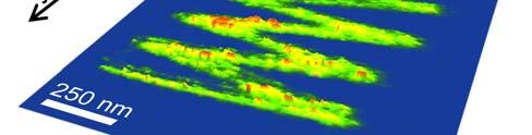
6 An important goal of this work was to demonstrate variable reduction of GO. Friction measurements show that this could be achieved by controlling the temperature of the AFM tip. Graphene has a low friction coefficient (32) while oxides typically have higher friction coefficients. Consequently, thermal reduction should also reduce friction as the high friction GO is replaced with lower friction graphene. Figure 2 shows the strong correlation between the cantilever temperature during TCNL processing and the lateral force on a room temperature tip scanned over previously reduced squares. While the cantilever temperature can be precisely determined, the contact temperature must be modeled (see Supporting Online Material). The reported temperatures are the cantilever temperatures. Reduction begins at or above 130 C which is comparable to the results of Wu et al. and Mattevi et al. that showed that reduction starts at 100 C (15, 26) presumably after the desorption of adventitious water. Higher temperatures increased the rate of reduction as shown by the roughly linear decrease in relative friction with temperature. Although isolated GO flakes are suited for basic studies of the process, further technological development requires extended films of GO. Large area GO epi films (> 15 mm 2 ) are obtained by oxidizing multilayer epitaxial graphene (EG) grown on the carbon face of SiC (28). The oxidized films consist of multiple high-quality GO epi layers that completely cover the SiC surface. AFM images show no tearing in the GO epi films indicating that they maintain their structural integrity when exposed to the harsh oxidation conditions. Figures 3 and 4 show the results obtained by performing TCNL on a GO epi film with a thickness of about 25 ± 5 nm, as determined by AFM by scratching - 5 -
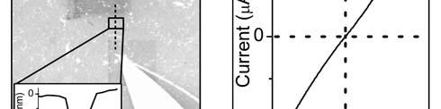
7 away GO epi from the SiC substrate. Figure 3 presents a zigzag rgo epi nanoribbon written with a single line scan at T heater ~ 1060 C on GO epi. Figure 3a is an image of the current measured between a conductive platinum AFM tip and each point of the surface, showing no current on the GO surface and a current enhancement of about 100 pa in the rgo epi nanoribbons. These current values are consistent with the presence of 12 nm wide and several nanometers thick rgo epi nanoribbons presenting a vanishingly small Schottky barrier; and a resistive SiC substrate (resistivity of about 10 5 Ω cm ). For a 25 nm thick GO film locally heated by a tip at 1000 C, heat flow through the layers might reduce most of the GO underneath the tip leaving only a few layers of unreduced GO at the SiC interface (see Supporting Online Material). The topographical image (Fig. 3b and black graph in Fig. 3c) indicates that the reduction produces a shallow indentation of 1 nm whose origin has been previously discussed for the isolated GO sheets. We further investigated the electrical properties of the locally reduced GO epi structures using KPFM and 4-point transport measurements in a UHV Omicron Nanoprobe system (see Supporting Online Material). In the 4-point transport measurements (Fig. 4a and 4b), we measured the sheet resistance, R sheet, of μm 2 squares of TCNL rgo epi and found that R sheet decreased with increasing temperature used for the TCNL local reduction, up to four orders of magnitude lower than the resistance of the original GO epi (15). The same significant increase of the in-plane conductivity is observed for extended films of rgo epi produced by overnight heating of GO epi in a furnace at 600 o C. Furthermore, we found that R sheet and the shape of the I(V) characteristics can be varied by changing the temperature of the AFM probe (see Fig. 4a and 4b), consistent with a change in the - 6 -
8 transport gap from 0.5 ev to vanishingly small. These results are consistent with KPFM measurements showing that the TCNL reduced GO epi displays a contact potential change of 168 ± 54 mv in respect to GO epi. Due to the residual oxygen and structural disorder, we observe a large difference in conductivity between epitaxial graphene and rgo epi or TCNL-rGO epi. Having established that heated tips achieved reductions comparable to global heating treatments, we extended the analysis to an isolated TCNL-rGO epi nanoribbon (Fig. 4c). The TCNL-rGO epi nanoribbon had a length, L, of 25 μm and a width, w, of 100 nm as measured by AFM. Current versus voltage data were acquired in the Omicron Nanoprobe system by placing the conductive tips on top of two micron-size squares of rgo epi fabricated in situ by an electron beam at each end of the nanoribbon (Fig. 4c). These pads ensured good electrical contact with the narrow ribbon. Two point transport measurements indicated a resistance larger than 2 GΩ when the tips were positioned on an arbitrary position on the GO surface (very large barrier at the contact) and a drop in resistance from 120 MΩ (between the 2 squares with no nanoribbon) to 20 MΩ (between the 2 squares connected by the nanoribbon). More importantly the transport behavior changes from insulating to ohmic (linear I(V) curves) in presence of the TCNL-rGO epi nanoribbon between the squares (Fig. 4c). By using the relationship R sheet = (R ribbon w t ribbon ) / (L t sheet ) (33), and assuming a 13 nm thick nanoribbon, we obtain a sheet resistance of 65 kω, in very good agreement with the measurements reported in Fig. 4 a, and b for microscopic squares of TCNL-rGO epi
9 A tip-based thermochemical nanolithography has been developed to directly control the electrical properties of GO on the nanoscale at speeds of several micrometers per seconds. Arbitrary shapes of reduced GO features can be produced by this technique. Compared to the starting GO, the rgo nanostructures, with widths down to 12 nm, show an increase in conductivity up to four orders of magnitude and a change in the shape of the I(V) characteristics. Dozens of arbitrarily shaped rgo features have been produced in arbitrarily chosen positions in the GO films, with a 100 percent yield, demonstrating the good reproducibility of the technique. The size of the rgo structures shown here was continuously varied between 12 nm (FWHM width of a nanoribbon) up to 20 μm. No sign of tip wear or sample tearing was observed, indicating that the "carbon skeleton" is continuous across the GO/rGO junction. As a result, extrinsic effects such as impurities, and interface layers, are likely obviated. Critically, TCNL does not require any solvents or lithographic resists that could contaminate the sample. This is especially important since the electronic properties of graphene are known to vary strongly with surface doping. Furthermore, the heatable probe enables in situ metrology of the fabricated nanostructures, such as friction, and Raman measurements. TCNL applied to large scale GO grown on SiC is a reliable, high resolution, no tearing technique which can be applied to conductive and non conductive substrates and which preserves the continuity of the carbon skeleton. The strategy of variably reducing extended GO films is a general one that could be implemented in multiple ways depending on the application. The manufacture of graphene nanoelectronics could be achieved by using arrays of heated probe tips (25). Independently addressed heated probe tips could alternately read or write - 8 -
10 nanostructures on a surface and in large arrays could address wafer-scale areas at high speed. A nano-embossing approach might also achieve local GO reduction, provided that the imprint template would offer nanometer-scale control of the reducing temperature field (34). Competing Financial Interests The authors declare that they have no competing financial interests
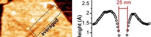
11 Figure legends Fig. 1. Local thermal reduction of a single-layered graphene oxide flake. (A) Topography of a cross shape of reduced GO formed after an AFM tip heats the contact to 330 C scanned across the GO sheet at 2 μm/s. (B) Zoom out topographical top view of the same sheet as that in (A). (C) The averaged profile of the trench outlined in (B) shows that the width (FWHM) of the line can be as narrow as 25 nm. Fig. 2. The rate of thermal reduction depends on the tip temperature. The plot shows the decrease in lateral force on an AFM tip at room temperature as it scans over several squares previously reduced by TCNL at different temperatures. The inset is a room temperature friction image of the GO sheet on which a heated tip was previously rastered twice over six square areas, at a speed of 4 μm/s. In square 1, the tip was heated during TCNL to T heater ~ 100 C yielding no apparent reduction while at temperatures T heater >150 C the rastered areas (2-6) were thermally reduced. Reduced GO, which like bulk graphite behaves as a lubricant, shows lower friction than the original GO. Higher temperatures accelerate the thermal reduction of GO and thereby more rapidly lower friction. Fig. 3. Local thermal reduction of a GO epi film: current and topographical images. (A) 3D room temperature AFM current image (taken with a bias voltage of 2.5V between tip and substrate) of a zigzag shaped nanoribbon fabricated by TCNL on GO epi at T heater ~ 1060 C, with a linear speed of 0.2 μm s -1 and a load of 120 nn. (B) Corresponding
12 topography image taken simultaneously with (A). (C) Averaged profiles of current and height of the cross sections that are indicated as dashed lines in (B). Fig and 2-point transport measurements and Kelvin probe force microscopy. (A) Current-voltage curves obtained by 4-point transport measurements of TCNL lowtemperature reduced graphene oxide (Low T, T heater ~ 600 C), TCNL high-temperature reduced graphene oxide (High T, T heater ~ 1200 C), and vacuum reduced graphene oxide at 600 o C. (B) This table presents the sheet resistance, R sheet, measured by 4-point transport measurements, and the contact potential change (ΔΦ) between GO epi and each listed sample (EG, rgo epi, and TCNL-rGO epi, respectively). (C) Left. SEM images of the configuration used for 2-point transport measurements when the tips are positioned between 2 rgo epi squares without (top), and with (bottom) TCNL-rGO epi nanoribbon in between. The AFM cross section of the nanoribbon is shown as inset of the bottom SEM image. Right. I(V) curves obtained measuring current between 2 rgo epi squares with no nanoribbon in between (top curve), and between 2 rgo epi squares with a nanoribbon in between (bottom curve)


13 Figures Figure


14 Figure


15 Figure


16 Figure
17 References and Notes: 1. M. Y. Han, B. Ozyilmaz, Y. B. Zhang, P. Kim, Phys. Rev. Lett. 98, (2007) 2. M. Orlita et al., Phys. Rev. Lett. 101, (2008). 3. X. Du, I. Skachko, A. Barker, E. Y. Andrei, Nat. Nanotechnol. 3, 491 (2008). 4. Y. B. Zhang, Y. W. Tan, H. L. Stormer, P. Kim, Nature 438, 201 (2005). 5. K. S. Novoselov et al., Science 306, 666 (2004). 6. C. Berger et al., J. Phys. Chem. B 108, (2004). 7. X. L. Li, X. R. Wang, L. Zhang, S. W. Lee, H. J. Dai, Science 319, 1229 (2008). 8. K. Nakada, M. Fujita, G. Dresselhaus, M. S. Dresselhaus, Phys. Rev. B 54, (1996). 9. J. Kedzierski et al., IEEE Trans. Electron Devices 55, 2078 (2008). 10. J. S. Moon et al., IEEE Electron Device Lett. 30, 650 (2009). 11. L. A. Ponomarenko et al., Science 320, 356 (2008). 12. L. S. Weng, L. Y. Zhang, Y. P. Chen, L. P. Rokhinson, Appl. Phys. Lett. 93, (2008). 13. L. Y. Jiao, L. Zhang, X. R. Wang, G. Diankov, H. J. Dai, Nature 458, 877 (2009). 14. G. Eda, G. Fanchini, M. Chhowalla, Nat. Nanotechnol. 3, 270 (2008). 15. X. S. Wu et al., Phys. Rev. Lett. 101, (2008). 16. J. T. Robinson, F. K. Perkins, E. S. Snow, Z. Q. Wei, P. E. Sheehan, Nano Lett. 8, 3137 (2008). 17. J. T. Robinson et al., Nano Lett. 8, 3441 (2008)
18 18. G. Eda, C. Mattevi, H. Yamaguchi, H. Kim, M. Chhowalla, J. Phys. Chem. C 113, (2009). 19. R. Szoszkiewicz et al., Nano Lett. 7, 1064 (2007). 20. D. Wang et al., Appl. Phys. Lett. 91, (2007). 21. D. Wang et al., Adv. Funct. Mater. 19, 3696 (2009). 22. P. E. Sheehan, L. J. Whitman, W. P. King, B. A. Nelson, Appl. Phys. Lett. 85, 1589 (2004). 23. M. Yang, P. E. Sheehan, W. P. King, L. J. Whitman, J. Am. Chem. Soc. 128, 6774 (2006). 24. B. A. Nelson, W. P. King, A. R. Laracuente, P. E. Sheehan, L. J. Whitman, Appl. Phys. Lett. 88, (2006). 25. P. Vettiger et al., IEEE T. Nanotechnol. 1, 39 (2002). 26. C. Mattevi et al., Adv. Funct. Mater. 19, 2577 (2009). 27. C. Gomez-Navarro et al., Nano Lett. 7, 3499 (2007). 28. Epitaxial graphene layers were grown on the C-face of 4H-SiC. GO epi was obtained by direct oxidation of the epitaxial graphene films on (16 layers in Fig. 4A, and 4B, and 13 layers in Fig.4C) chip, as described in reference (15). TCNL was performed in N 2 environment (Fig. 1 and 2) or ambient conditions (Fig. 3 and 4) using an AFM (Veeco Multimode III (Fig. 1 and 2) and IV (Fig. 3 and 4)) and custom made heated AFM probes (29) (nominal spring constant of 0.5 N m -1 ). During TCNL, the probe was heated while in contact with the GO surface at loading forces ranging between nn. The calibration of the temperature at
19 the top of the tip, T heater, and the estimation of the temperature at the tip-go interface, T local, is described in the online supporting material. All friction and electrical characterizations were performed at room temperature. 29. J. Lee et al., J. Microelectromech. Syst. 15, 1644 (2006). 30. H. C. Schniepp et al., J. Phys. Chem. B 110, 8535 (2006). 31. J. C. Meyer et al., Nature 446, 60 (2007). 32. T. Filleter et al., Phys. Rev. Lett. 102, (2009). 33. The thickness of the ribbon, t ribbon, and the thickness of the sheet, t sheet, have been inferred from the thickness of the corresponding GO films as reported in the online supplementary material. 34. This work has been supported by the National Science Foundation (CMDITR program DMR , MRSEC program DMR , and DMR ), Department of Energy (DE-FG02-06ER46293 and PECASE), the Institute for Nanoscience at Naval Research Laboratory, the Office of Naval Research of the United States, and Georgia Institute of Technology (Georgia Tech Research Foundation, COE Cutting Edge Research Award, and COPE fellowship). This research was performed while Z.W. held a National Research Council Research Associateship Award at Naval Research Laboratory of the United States. ZW thanks Dr. Hua Qi at NRL for providing doped silicon wafers, evaporating gold layers on mica, and taking SEM images of GO sheets on gold and silicon substrates
Supplementary Figure S1. AFM images of GraNRs grown with standard growth process. Each of these pictures show GraNRs prepared independently,
 Supplementary Figure S1. AFM images of GraNRs grown with standard growth process. Each of these pictures show GraNRs prepared independently, suggesting that the results is reproducible. Supplementary Figure
SUPPLEMENTARY INFORMATION
 SUPPLEMENTARY INFORMATION Facile Synthesis of High Quality Graphene Nanoribbons Liying Jiao, Xinran Wang, Georgi Diankov, Hailiang Wang & Hongjie Dai* Supplementary Information 1. Photograph of graphene
AC Electrothermal Characterization of Doped-Si Heated Microcantilevers Using Frequency-Domain Finite Element Analysis
 AC Electrothermal Characterization of Doped-Si Heated Microcantilevers Using Frequency-Domain Finite Element Analysis K. Park 1, S. Hamian 1, A. M. Gauffreau 2, T. Walsh 2 1 University of Utah, Salt Lake
Solvothermal Reduction of Chemically Exfoliated Graphene Sheets
 Solvothermal Reduction of Chemically Exfoliated Graphene Sheets Hailiang Wang, Joshua Tucker Robinson, Xiaolin Li, and Hongjie Dai* Department of Chemistry and Laboratory for Advanced Materials, Stanford
Case report on the article Water nanoelectrolysis: A simple model, Journal of Applied Physics (2017) 122,
 122,") Case report on the article Water nanoelectrolysis: A simple model, Journal of Applied Physics (2017) 122, 244902 Juan Olives, Zoubida Hammadi, Roger Morin, Laurent Lapena To cite this version: Juan Olives,
Case report on the article Water nanoelectrolysis: A simple model, Journal of Applied Physics (2017) 122, 244902 Juan Olives, Zoubida Hammadi, Roger Morin, Laurent Lapena To cite this version: Juan Olives,
Scalable templated growth of graphene nanoribbons on SiC
 Scalable templated growth of graphene nanoribbons on SiC Mike Sprinkle, Ming Ruan, Yike Hu, John H. Hankinson, Miguel Rubio-Roy, Baiqian Zhang, Xiaosong Wu, Claire Berger, Walt. A. De Heer To cite this
Frictional characteristics of exfoliated and epitaxial graphene
 Frictional characteristics of exfoliated and epitaxial graphene Young Jun Shin a,b, Ryan Stromberg c, Rick Nay c, Han Huang d, Andrew T. S. Wee d, Hyunsoo Yang a,b,*, Charanjit S. Bhatia a a Department
Trench IGBT failure mechanisms evolution with temperature and gate resistance under various short-circuit conditions
 Trench IGBT failure mechanisms evolution with temperature and gate resistance under various short-circuit conditions Adel Benmansour, Stephane Azzopardi, Jean-Christophe Martin, Eric Woirgard To cite this
Wafer-scale fabrication of graphene
 Wafer-scale fabrication of graphene Sten Vollebregt, MSc Delft University of Technology, Delft Institute of Mircosystems and Nanotechnology Delft University of Technology Challenge the future Delft University
Exceptional ballistic transport in epigraphene. Walt de Heer Georgia Institute of Technology
 Exceptional ballistic transport in epigraphene Walt de Heer Georgia Institute of Technology Program Objective First formulated in 2001 and patented in 2003, our objective is to develop nanoelectronics
Proposal of A New Structure Thermal Vacuum Sensor with Diode-Thermistors Combined with a Micro-Air-Bridge Heater
 Proposal of A New Structure Thermal Vacuum Sensor with Diode-Thermistors Combined with a Micro-Air-Bridge Heater M. Kimura, F. Sakurai, H. Ohta, T. Terada To cite this version: M. Kimura, F. Sakurai, H.
SUPPLEMENTARY NOTES Supplementary Note 1: Fabrication of Scanning Thermal Microscopy Probes
 SUPPLEMENTARY NOTES Supplementary Note 1: Fabrication of Scanning Thermal Microscopy Probes Fabrication of the scanning thermal microscopy (SThM) probes is summarized in Supplementary Fig. 1 and proceeds
Thermal conductivity of semiconductor superlattices: Experimental study of interface scattering
 Thermal conductivity of semiconductor superlattices: Experimental study of interface scattering Jean Yves Duquesne To cite this version: Jean Yves Duquesne. Thermal conductivity of semiconductor superlattices:
Interactions of an eddy current sensor and a multilayered structure
 Interactions of an eddy current sensor and a multilayered structure Thanh Long Cung, Pierre-Yves Joubert, Eric Vourc H, Pascal Larzabal To cite this version: Thanh Long Cung, Pierre-Yves Joubert, Eric
Sub-5 nm Patterning and Applications by Nanoimprint Lithography and Helium Ion Beam Lithography
 Sub-5 nm Patterning and Applications by Nanoimprint Lithography and Helium Ion Beam Lithography Yuanrui Li 1, Ahmed Abbas 1, Yuhan Yao 1, Yifei Wang 1, Wen-Di Li 2, Chongwu Zhou 1 and Wei Wu 1* 1 Department
Supplementary Figure 1 Dark-field optical images of as prepared PMMA-assisted transferred CVD graphene films on silicon substrates (a) and the one
 and the one") Supplementary Figure 1 Dark-field optical images of as prepared PMMA-assisted transferred CVD graphene films on silicon substrates (a) and the one after PBASE monolayer growth (b). 1 Supplementary Figure
Supplementary Figure 1 Dark-field optical images of as prepared PMMA-assisted transferred CVD graphene films on silicon substrates (a) and the one after PBASE monolayer growth (b). 1 Supplementary Figure
Carbon Nanotubes as Future Energy Storage System
 Carbon Nanotubes as Future Energy Storage System V Vasu, D Silambarasan To cite this version: V Vasu, D Silambarasan. Carbon Nanotubes as Future Energy Storage System. Mechanics, Materials Science Engineering
Fundamental Benefits of the Staggered Geometry for Organic Field-Effect Transistors
 Fundamental Benefits of the Staggered Geometry for Organic Field-Effect Transistors Chang Hyun Kim, Yvan Bonnassieux, Gilles Horowitz To cite this version: Chang Hyun Kim, Yvan Bonnassieux, Gilles Horowitz.
Smart Bolometer: Toward Monolithic Bolometer with Smart Functions
 Smart Bolometer: Toward Monolithic Bolometer with Smart Functions Matthieu Denoual, Gilles Allègre, Patrick Attia, Olivier De Sagazan To cite this version: Matthieu Denoual, Gilles Allègre, Patrick Attia,
Supporting Online Material for
 www.sciencemag.org/cgi/content/full/327/5966/662/dc Supporting Online Material for 00-GHz Transistors from Wafer-Scale Epitaxial Graphene Y.-M. Lin,* C. Dimitrakopoulos, K. A. Jenkins, D. B. Farmer, H.-Y.
0.9 ev POTENTIAL BARRIER SCHOTTKY DIODE ON ev GAP GaxIn1-xASSi:H
 0.9 ev POTENTIAL BARRIER SCHOTTKY DIODE ON 0.75-0.5 ev GAP GaxIn1-xASSi:H A. Deneuville, F. Valentin, S. Belkouch To cite this version: A. Deneuville, F. Valentin, S. Belkouch. 0.9 ev POTENTIAL BARRIER
NiCl2 Solution concentration. Etching Duration. Aspect ratio. Experiment Atmosphere Temperature. Length(µm) Width (nm) Ar:H2=9:1, 150Pa
 Width (nm) Ar:H2=9:1, 150Pa") Experiment Atmosphere Temperature #1 # 2 # 3 # 4 # 5 # 6 # 7 # 8 # 9 # 10 Ar:H2=9:1, 150Pa Ar:H2=9:1, 150Pa Ar:H2=9:1, 150Pa Ar:H2=9:1, 150Pa Ar:H2=9:1, 150Pa Ar:H2=9:1, 150Pa Ar:H2=9:1, 150Pa Ar:H2=9:1,
Experiment Atmosphere Temperature #1 # 2 # 3 # 4 # 5 # 6 # 7 # 8 # 9 # 10 Ar:H2=9:1, 150Pa Ar:H2=9:1, 150Pa Ar:H2=9:1, 150Pa Ar:H2=9:1, 150Pa Ar:H2=9:1, 150Pa Ar:H2=9:1, 150Pa Ar:H2=9:1, 150Pa Ar:H2=9:1,
Investigation of nanoelectrodes by Transmission Electron Microscopy
 Investigation of nanoelectrodes by Transmission Electron Microscopy M.S. Kabir, S.H.M. Persson, Yimin Yao, Jean-Philippe Bourgoin, Serge Palacin To cite this version: M.S. Kabir, S.H.M. Persson, Yimin
Low Voltage Field Emission SEM (LV FE-SEM): A Promising Imaging Approach for Graphene Samples
: A Promising Imaging Approach for Graphene Samples") Low Voltage Field Emission SEM (LV FE-SEM): A Promising Imaging Approach for Graphene Samples Jining Xie Agilent Technologies May 23 rd, 2012 www.agilent.com/find/nano Outline 1. Introduction 2. Agilent
Low Voltage Field Emission SEM (LV FE-SEM): A Promising Imaging Approach for Graphene Samples Jining Xie Agilent Technologies May 23 rd, 2012 www.agilent.com/find/nano Outline 1. Introduction 2. Agilent
Open-Thru de-embedding for Graphene RF devices
 Open-Thru de-embedding for Graphene RF devices Giancarlo Vincenzi, Georgios Deligeorgis, Fabio Coccetti, Patrick Pons To cite this version: Giancarlo Vincenzi, Georgios Deligeorgis, Fabio Coccetti, Patrick
Supplementary Figure 1 Experimental setup for crystal growth. Schematic drawing of the experimental setup for C 8 -BTBT crystal growth.
 Supplementary Figure 1 Experimental setup for crystal growth. Schematic drawing of the experimental setup for C 8 -BTBT crystal growth. Supplementary Figure 2 AFM study of the C 8 -BTBT crystal growth
Electromagnetic characterization of magnetic steel alloys with respect to the temperature
 Electromagnetic characterization of magnetic steel alloys with respect to the temperature B Paya, P Teixeira To cite this version: B Paya, P Teixeira. Electromagnetic characterization of magnetic steel
Spatially resolving density-dependent screening around a single charged atom in graphene
 Supplementary Information for Spatially resolving density-dependent screening around a single charged atom in graphene Dillon Wong, Fabiano Corsetti, Yang Wang, Victor W. Brar, Hsin-Zon Tsai, Qiong Wu,
Initial Stages of Growth of Organic Semiconductors on Graphene
 Initial Stages of Growth of Organic Semiconductors on Graphene Presented by: Manisha Chhikara Supervisor: Prof. Dr. Gvido Bratina University of Nova Gorica Outline Introduction to Graphene Fabrication
Graphene Fundamentals and Emergent Applications
 Graphene Fundamentals and Emergent Applications Jamie H. Warner Department of Materials University of Oxford Oxford, UK Franziska Schaffel Department of Materials University of Oxford Oxford, UK Alicja
EFFECT OF TIP-SIZE ON STM IMAGES OF GRAPHITE
 EFFECT OF TIP-SIZE ON STM IMAGES OF GRAPHITE C. Horie, H. Miyazaki To cite this version: C. Horie, H. Miyazaki. EFFECT OF TIP-SIZE ON STM IMAGES OF GRAPHITE. Journal de Physique Colloques, 1987, 48 (C6),
SUPPLEMENTARY INFORMATION
 Supplementary Information: Photocurrent generation in semiconducting and metallic carbon nanotubes Maria Barkelid 1*, Val Zwiller 1 1 Kavli Institute of Nanoscience, Delft University of Technology, Delft,
Mirage detection for electrochromic materials characterization. Application to iridium oxide films
 Mirage detection for electrochromic materials characterization. Application to iridium oxide films V. Plichon, M. Petit To cite this version: V. Plichon, M. Petit. Mirage detection for electrochromic materials
Carbon based Nanoscale Electronics
 Carbon based Nanoscale Electronics 09 02 200802 2008 ME class Outline driving force for the carbon nanomaterial electronic properties of fullerene exploration of electronic carbon nanotube gold rush of
Particle-in-cell simulations of high energy electron production by intense laser pulses in underdense plasmas
 Particle-in-cell simulations of high energy electron production by intense laser pulses in underdense plasmas Susumu Kato, Eisuke Miura, Mitsumori Tanimoto, Masahiro Adachi, Kazuyoshi Koyama To cite this
Full-order observers for linear systems with unknown inputs
 Full-order observers for linear systems with unknown inputs Mohamed Darouach, Michel Zasadzinski, Shi Jie Xu To cite this version: Mohamed Darouach, Michel Zasadzinski, Shi Jie Xu. Full-order observers
HIGH RESOLUTION ION KINETIC ENERGY ANALYSIS OF FIELD EMITTED IONS
 HIGH RESOLUTION ION KINETIC ENERGY ANALYSIS OF FIELD EMITTED IONS J. Liu, T. Tsong To cite this version: J. Liu, T. Tsong. HIGH RESOLUTION ION KINETIC ENERGY ANALYSIS OF FIELD EMITTED IONS. Journal de
Direct-writing on monolayer GO with Pt-free AFM tips in the
 Supplementary Figure S1 Direct-writing on monolayer GO with Pt-free AFM tips in the presence of hydrogen. We replaced the Pt-coated tip with a gold-coated tip or an untreated fresh silicon tip, and kept
Evaluation of transverse elastic properties of fibers used in composite materials by laser resonant ultrasound spectroscopy
 Evaluation of transverse elastic properties of fibers used in composite materials by laser resonant ultrasound spectroscopy Denis Mounier, Christophe Poilâne, Cécile Bûcher, Pascal Picart To cite this
Nanometer-Scale Materials Contrast Imaging with a Near-Field Microwave Microscope
 Nanometer-Scale Materials Contrast Imaging with a Near-Field Microwave Microscope Atif Imtiaz 1 and Steven M. Anlage Center for Superconductivity Research, Department of Physics, University of Maryland,
Precision Cutting and Patterning of Graphene with Helium Ions. 1.School of Engineering and Applied Sciences, Harvard University, Cambridge MA 02138
 Precision Cutting and Patterning of Graphene with Helium Ions D.C. Bell 1,2, M.C. Lemme 3, L. A. Stern 4, J.R. Williams 1,3, C. M. Marcus 3 1.School of Engineering and Applied Sciences, Harvard University,
A new simple recursive algorithm for finding prime numbers using Rosser s theorem
 A new simple recursive algorithm for finding prime numbers using Rosser s theorem Rédoane Daoudi To cite this version: Rédoane Daoudi. A new simple recursive algorithm for finding prime numbers using Rosser
TRANSVERSE SPIN TRANSPORT IN GRAPHENE
 International Journal of Modern Physics B Vol. 23, Nos. 12 & 13 (2009) 2641 2646 World Scientific Publishing Company TRANSVERSE SPIN TRANSPORT IN GRAPHENE TARIQ M. G. MOHIUDDIN, A. A. ZHUKOV, D. C. ELIAS,
Easter bracelets for years
 Easter bracelets for 5700000 years Denis Roegel To cite this version: Denis Roegel. Easter bracelets for 5700000 years. [Research Report] 2014. HAL Id: hal-01009457 https://hal.inria.fr/hal-01009457
Surface atoms/molecules of a material act as an interface to its surrounding environment;
 1 Chapter 1 Thesis Overview Surface atoms/molecules of a material act as an interface to its surrounding environment; their properties are often complicated by external adsorbates/species on the surface
Transparent Electrode Applications
 Transparent Electrode Applications LCD Solar Cells Touch Screen Indium Tin Oxide (ITO) Zinc Oxide (ZnO) - High conductivity - High transparency - Resistant to environmental effects - Rare material (Indium)
FIM OBSERVATION OF MONOLAYER Pd ADSORBED ON W AND Mo SURFACES
 FIM OBSERVATION OF MONOLAYER Pd ADSORBED ON W AND Mo SURFACES K. Okuno, H. Kim To cite this version: K. Okuno, H. Kim. FIM OBSERVATION OF MONOLAYER Pd ADSORBED ON W AND Mo SURFACES. Journal de Physique
(a) (b) Supplementary Figure 1. (a) (b) (a) Supplementary Figure 2. (a) (b) (c) (d) (e)
 (b) Supplementary Figure 1. (a) (b) (a) Supplementary Figure 2. (a) (b) (c) (d) (e)") (a) (b) Supplementary Figure 1. (a) An AFM image of the device after the formation of the contact electrodes and the top gate dielectric Al 2 O 3. (b) A line scan performed along the white dashed line
(a) (b) Supplementary Figure 1. (a) An AFM image of the device after the formation of the contact electrodes and the top gate dielectric Al 2 O 3. (b) A line scan performed along the white dashed line
IMPROVEMENTS OF THE VARIABLE THERMAL RESISTANCE
 IMPROVEMENTS OF THE VARIABLE THERMAL RESISTANCE V. Szekely, S. Torok, E. Kollar To cite this version: V. Szekely, S. Torok, E. Kollar. IMPROVEMENTS OF THE VARIABLE THERMAL RESIS- TANCE. THERMINIC 2007,
Dispersion relation results for VCS at JLab
 Dispersion relation results for VCS at JLab G. Laveissiere To cite this version: G. Laveissiere. Dispersion relation results for VCS at JLab. Compton Scattering from Low to High Momentum Transfer, Mar
Transport through Andreev Bound States in a Superconductor-Quantum Dot-Graphene System
 Transport through Andreev Bound States in a Superconductor-Quantum Dot-Graphene System Nadya Mason Travis Dirk, Yung-Fu Chen, Cesar Chialvo Taylor Hughes, Siddhartha Lal, Bruno Uchoa Paul Goldbart University
Design and Simulation of Cantilever Based MEMS Bimorph Piezoelectric Energy Harvester
 Design and Simulation of Cantilever Based MEMS Bimorph Piezoelectric Harvester G.K.S Prakash Raju, P Ashok Kumar, K Srinivasa Rao, Vanaja Aravapalli To cite this version: G.K.S Prakash Raju, P Ashok Kumar,
Interferences of Peltier thermal waves produced in ohmic contacts upon integrated circuits
 Interferences of Peltier thermal waves produced in ohmic contacts upon integrated circuits W. Claeys, S. Dilhaire, V. Quintard, D. Lewis, T. Phan, J. Aucouturier To cite this version: W. Claeys, S. Dilhaire,
Methylation-associated PHOX2B gene silencing is a rare event in human neuroblastoma.
 Methylation-associated PHOX2B gene silencing is a rare event in human neuroblastoma. Loïc De Pontual, Delphine Trochet, Franck Bourdeaut, Sophie Thomas, Heather Etchevers, Agnes Chompret, Véronique Minard,
Supplementary Figure 1: Micromechanical cleavage of graphene on oxygen plasma treated Si/SiO2. Supplementary Figure 2: Comparison of hbn yield.
 1 2 3 4 Supplementary Figure 1: Micromechanical cleavage of graphene on oxygen plasma treated Si/SiO 2. Optical microscopy images of three examples of large single layer graphene flakes cleaved on a single
Supporting Information Available:
 Supporting Information Available: Photoresponsive and Gas Sensing Field-Effect Transistors based on Multilayer WS 2 Nanoflakes Nengjie Huo 1, Shengxue Yang 1, Zhongming Wei 2, Shu-Shen Li 1, Jian-Bai Xia
Water Vapour Effects in Mass Measurement
 Water Vapour Effects in Mass Measurement N.-E. Khélifa To cite this version: N.-E. Khélifa. Water Vapour Effects in Mass Measurement. Measurement. Water Vapour Effects in Mass Measurement, May 2007, Smolenice,
Heiba Zaghloul, G. Papaioannou, Fabio Coccetti, Patrick Pons, Robert Plana. To cite this version:
 Effect of Humidity on Dielectric Charging Process in Electrostatic Capacitive RF MEMS Switches Based on Kelvin Probe Force Microscopy Surface Potential Measurements Heiba Zaghloul, G. Papaioannou, Fabio
High-resolution Characterization of Organic Ultrathin Films Using Atomic Force Microscopy
 High-resolution Characterization of Organic Ultrathin Films Using Atomic Force Microscopy Jing-jiang Yu Nanotechnology Measurements Division Agilent Technologies, Inc. Atomic Force Microscopy High-Resolution
Characterization of the local Electrical Properties of Electrical Machine Parts with non-trivial Geometry
 Characterization of the local Electrical Properties of Electrical Machine Parts with non-trivial Geometry Laure Arbenz, Abdelkader Benabou, Stéphane Clenet, Jean Claude Mipo, Pierre Faverolle To cite this
Crystalline Surfaces for Laser Metrology
 Crystalline Surfaces for Laser Metrology A.V. Latyshev, Institute of Semiconductor Physics SB RAS, Novosibirsk, Russia Abstract: The number of methodological recommendations has been pronounced to describe
Long Term H-Release from Amorphous Carbon Evidenced by in Situ Raman Microscopy under Isothermal Heating
 Long Term H-Release from Amorphous Carbon Evidenced by in Situ Raman Microscopy under Isothermal Heating Cedric Pardanaud, C. Martin, G. Giacometti, P. Roubin, B. Pégourié, C. Hopf, T. Schwarz-Selinger,
Intrinsic Electronic Transport Properties of High. Information
 Intrinsic Electronic Transport Properties of High Quality and MoS 2 : Supporting Information Britton W. H. Baugher, Hugh O. H. Churchill, Yafang Yang, and Pablo Jarillo-Herrero Department of Physics, Massachusetts
On the beam deflection method applied to ultrasound absorption measurements
 On the beam deflection method applied to ultrasound absorption measurements K. Giese To cite this version: K. Giese. On the beam deflection method applied to ultrasound absorption measurements. Journal
Journal Name. Supporting Information. Significant enhancement in blue emission and electrical conductivity of N-doped graphene. Dynamic Article Links
 Journal Name Dynamic Article Links Cite this: DOI:.39/c0xx00000x www.rsc.org/xxxxxx Supporting Information Significant enhancement in blue emission and electrical conductivity of N-doped graphene Tran
Antipodal radiation pattern of a patch antenna combined with superstrate using transformation electromagnetics
 Antipodal radiation pattern of a patch antenna combined with superstrate using transformation electromagnetics Mark Clemente Arenas, Anne-Claire Lepage, Xavier Begaud To cite this version: Mark Clemente
Stator/Rotor Interface Analysis for Piezoelectric Motors
 Stator/Rotor Interface Analysis for Piezoelectric Motors K Harmouch, Yves Bernard, Laurent Daniel To cite this version: K Harmouch, Yves Bernard, Laurent Daniel. Stator/Rotor Interface Analysis for Piezoelectric
Numerical Modeling of Eddy Current Nondestructive Evaluation of Ferromagnetic Tubes via an Integral. Equation Approach
 Numerical Modeling of Eddy Current Nondestructive Evaluation of Ferromagnetic Tubes via an Integral Equation Approach Anastassios Skarlatos, Grégoire Pichenot, Dominique Lesselier, Marc Lambert, Bernard
Fabrication and Domain Imaging of Iron Magnetic Nanowire Arrays
 Abstract #: 983 Program # MI+NS+TuA9 Fabrication and Domain Imaging of Iron Magnetic Nanowire Arrays D. A. Tulchinsky, M. H. Kelley, J. J. McClelland, R. Gupta, R. J. Celotta National Institute of Standards
M R S Internet Journal of Nitride Semiconductor Research
 Page 1 of 6 M R S Internet Journal of Nitride Semiconductor Research Volume 9, Article 7 The Ambient Temperature Effect on Current-Voltage Characteristics of Surface-Passivated GaN-Based Field-Effect Transistors
Predicting the risk of non-compliance to EMC requirements during the life-cycle
 Predicting the risk of non-compliance to EMC requirements during the life-cycle Alexandre Boyer, He Huang, Sonia Ben Dhia To cite this version: Alexandre Boyer, He Huang, Sonia Ben Dhia. Predicting the
Vibro-acoustic simulation of a car window
 Vibro-acoustic simulation of a car window Christophe Barras To cite this version: Christophe Barras. Vibro-acoustic simulation of a car window. Société Française d Acoustique. Acoustics 12, Apr 12, Nantes,
Greg Andreev and Aravind Vijayaraghavan 9/27/13
 Mapping Graphene s surface potential with
ELASTIC PROPERTIES OF THE ONE-DIMENSIONAL METAL Mo2 S3
 ELASTIC PROPERTIES OF THE ONE-DIMENSIONAL METAL Mo2 S3 Alova, G. Mozurkewich To cite this version: Alova, G. Mozurkewich. ELASTIC PROPERTIES OF THE ONE-DIMENSIONAL METAL Mo2 S3. Journal de Physique Colloques,
Raman spectroscopy at the edges of multilayer graphene
 Raman spectroscopy at the edges of multilayer graphene Q. -Q. Li, X. Zhang, W. -P. Han, Y. Lu, W. Shi, J. -B. Wu, P. -H. Tan* State Key Laboratory of Superlattices and Microstructures, Institute of Semiconductors,
DESIGN AND FABRICATION OF A MICRO ELECTROSTATIC VIBRATION-TO-ELECTRICITY ENERGY CONVERTER
 DESIGN AND FABRICATION OF A MICRO ELECTROSTATIC IBRATION-TO-ELECTRICITY ENERGY CONERTER Yi Chiu, Chiung-Ting Kuo, Yu-Shan Chu To cite this version: Yi Chiu, Chiung-Ting Kuo, Yu-Shan Chu. DESIGN AND FABRICATION
Etching of Graphene Devices with a Helium Ion Beam
 Etching of Graphene Devices with a Helium Ion Beam The Harvard community has made this article openly available. Please share how this access benefits you. Your story matters Citation Lemme, Max C., David
On size, radius and minimum degree
 On size, radius and minimum degree Simon Mukwembi To cite this version: Simon Mukwembi. On size, radius and minimum degree. Discrete Mathematics and Theoretical Computer Science, DMTCS, 2014, Vol. 16 no.
Efficient Preparation of Large-Area Graphene Oxide Sheets for Transparent Conductive Films
 Supporting Information Efficient Preparation of Large-Area Graphene Oxide Sheets for Transparent Conductive Films Jinping Zhao, Songfeng Pei, Wencai Ren*, Libo Gao and Hui-Ming Cheng* Shenyang National
Supporting Information. by Hexagonal Boron Nitride
 Supporting Information High Velocity Saturation in Graphene Encapsulated by Hexagonal Boron Nitride Megan A. Yamoah 1,2,, Wenmin Yang 1,3, Eric Pop 4,5,6, David Goldhaber-Gordon 1 * 1 Department of Physics,
A. Optimizing the growth conditions of large-scale graphene films
 1 A. Optimizing the growth conditions of large-scale graphene films Figure S1. Optical microscope images of graphene films transferred on 300 nm SiO 2 /Si substrates. a, Images of the graphene films grown
Estimation and Modeling of the Full Well Capacity in Pinned Photodiode CMOS Image Sensors
 Estimation and Modeling of the Full Well Capacity in Pinned Photodiode CMOS Image Sensors Alice Pelamatti, Vincent Goiffon, Magali Estribeau, Paola Cervantes, Pierre Magnan To cite this version: Alice
Using Heatable AFM Probes for the Nanolithography of Polymers, Nanoparticles, and Graphene. Paul Sheehan U.S. Naval Research Laboratory
 Using Heatable AFM Probes for the Nanolithography of Polymers, Nanoparticles, and Graphene Paul Sheehan U.S. Naval Research Laboratory Heatable Cantilevers [King Group, UIUC] Heating is controlled by passing
High Performance, Low Operating Voltage n-type Organic Field Effect Transistor Based on Inorganic-Organic Bilayer Dielectric System
 Journal of Physics: Conference Series PAPER OPEN ACCESS High Performance, Low Operating Voltage n-type Organic Field Effect Transistor Based on Inorganic-Organic Bilayer Dielectric System To cite this
ATOMIC STRUCTURE OF INTERFACES IN GaAs/Ga1-xAlxAs SUPERLATTICES
 ATOMIC STRUCTURE OF INTERFACES IN GaAs/Ga1-xAlxAs SUPERLATTICES J. Laval, C. Delamarre, A. Dubon, G. Schiffmacher, G. Teste de Sagey, B. Guenais, A. Regreny To cite this version: J. Laval, C. Delamarre,
Instrumentation and Operation
 Instrumentation and Operation 1 STM Instrumentation COMPONENTS sharp metal tip scanning system and control electronics feedback electronics (keeps tunneling current constant) image processing system data
Raman Imaging and Electronic Properties of Graphene
 Raman Imaging and Electronic Properties of Graphene F. Molitor, D. Graf, C. Stampfer, T. Ihn, and K. Ensslin Laboratory for Solid State Physics, ETH Zurich, 8093 Zurich, Switzerland ensslin@phys.ethz.ch
SUPPLEMENTARY INFORMATION
 Engineered doping of organic semiconductors for enhanced thermoelectric efficiency G.-H. Kim, 1 L. Shao, 1 K. Zhang, 1 and K. P. Pipe 1,2,* 1 Department of Mechanical Engineering, University of Michigan,
Eddy-Current Effects in Circuit Breakers During Arc Displacement Phase
 Eddy-Current Effects in Circuit Breakers During Arc Displacement Phase Olivier Chadebec, Gerard Meunier, V. Mazauric, Yann Le Floch, Patrice Labie To cite this version: Olivier Chadebec, Gerard Meunier,
Black phosphorus: A new bandgap tuning knob
 Black phosphorus: A new bandgap tuning knob Rafael Roldán and Andres Castellanos-Gomez Modern electronics rely on devices whose functionality can be adjusted by the end-user with an external knob. A new
Hopping in CVD Grown Single-layer MoS 2
 Supporting Information for Large Thermoelectricity via Variable Range Hopping in CVD Grown Single-layer MoS 2 Jing Wu 1,2,3, Hennrik Schmidt 1,2, Kiran Kumar Amara 4, Xiangfan Xu 5, Goki Eda 1,2,4, and
Thomas Lugand. To cite this version: HAL Id: tel
 Contribution à la Modélisation et à l Optimisation de la Machine Asynchrone Double Alimentation pour des Applications Hydrauliques de Pompage Turbinage Thomas Lugand To cite this version: Thomas Lugand.
b-chromatic number of cacti
 b-chromatic number of cacti Victor Campos, Claudia Linhares Sales, Frédéric Maffray, Ana Silva To cite this version: Victor Campos, Claudia Linhares Sales, Frédéric Maffray, Ana Silva. b-chromatic number
Multicolor Graphene Nanoribbon/Semiconductor Nanowire. Heterojunction Light-Emitting Diodes
 Multicolor Graphene Nanoribbon/Semiconductor Nanowire Heterojunction Light-Emitting Diodes Yu Ye, a Lin Gan, b Lun Dai, *a Hu Meng, a Feng Wei, a Yu Dai, a Zujin Shi, b Bin Yu, a Xuefeng Guo, b and Guogang
OPTICAL CHARACTERIZATION OF Nd3+ DOPED CaF2 LAYERS GROWN BY MOLECULAR BEAM EPITAXY
 OPTICAL CHARACTERIZATION OF Nd3+ DOPED CaF2 LAYERS GROWN BY MOLECULAR BEAM EPITAXY L. Bausa, R. Legros, A. Munoz-Yague To cite this version: L. Bausa, R. Legros, A. Munoz-Yague. OPTICAL CHARACTERIZATION
FIELD EMISSION MICROSCOPY OF GALLIUM ARSENIDE
 FIELD EMISSION MICROSCOPY OF GALLIUM ARSENIDE C. Patel To cite this version: C. Patel. FIELD EMISSION MICROSCOPY OF GALLIUM ARSENIDE. Journal de Physique Colloques, 1986, 47 (C2), pp.c2-53-c2-58. .
Can we reduce health inequalities? An analysis of the English strategy ( )
") Can we reduce health inequalities? An analysis of the English strategy (1997-2010) Johan P Mackenbach To cite this version: Johan P Mackenbach. Can we reduce health inequalities? An analysis of the English
Can we reduce health inequalities? An analysis of the English strategy (1997-2010) Johan P Mackenbach To cite this version: Johan P Mackenbach. Can we reduce health inequalities? An analysis of the English
Lithography-free Fabrication of High Quality Substrate-supported and. Freestanding Graphene devices
 Lithography-free Fabrication of High Quality Substrate-supported and Freestanding Graphene devices W. Bao 1, G. Liu 1, Z. Zhao 1, H. Zhang 1, D. Yan 2, A. Deshpande 3, B.J. LeRoy 3 and C.N. Lau 1, * 1
An account of our efforts towards air quality monitoring in epitaxial graphene on SiC
 European Network on New Sensing Technologies for Air Pollution Control and Environmental Sustainability - EuNetAir COST Action TD1105 2 nd International Workshop EuNetAir on New Sensing Technologies for
MICRO-SCALE SHEET RESISTANCE MEASUREMENTS ON ULTRA SHALLOW JUNCTIONS
 MICRO-SCALE SHEET RESISTANCE MEASUREMENTS ON ULTRA SHALLOW JUNCTIONS Christian L. Petersen, Rong Lin, Dirch H. Petersen, Peter F. Nielsen CAPRES A/S, Burnaby, BC, Canada CAPRES A/S, Lyngby, Denmark We