Towards Si-based Light Sources. Greg Sun University of Massachusetts Boston
|
|
|
- Juliana Phelps
- 5 years ago
- Views:
Transcription
1 Towards Si-based Light Sources Greg Sun University of Massachusetts Boston


2 UMass System Amherst, Boston, Lowell, Dartmouth Worcester (Medical school)


3 UMass Boston

4


5 UMass Boston Established in 1964 Only public university in the city of Boston Undergraduate Students: 12K Graduate Students: 4K Thomas M. Menino, Bachelor of Arts in Community Planning (1988), UMass Boston, Mayor of Boston and the longestserving mayor in the history of the city
6 Outline Motivations Semiconductors (direct and indirect bandgap) Semiconductor laser diodes Challenges for light emissions from Si The group-iv (Si, Ge, Sn) band-to-band approach The group-iv intersubband approach Prospects of Si based lasers

7 What is a semiconductor? When bands are completely filled, they do not conduct current, only partially filled bands are conductive.
8 Direct and Indirect Bandgaps Eg Eg k k Direct bandgap: GaAs, InP, GaN Good for photonics Indirect bandgap: Si, Ge, AlAs Good for electronics
9 Photon Emissions from Semiconductors Conduction band Momentum Phonon emission Photon emission u l ħω In-plane k In-plane k Valence band 1) Light emitters require direct band gap 2) Wavelength is determined by the band gap

10 Band Structures of Real Semiconductors

11 Semiconductor Quantum Wells d Effective bandgap CB suband Bandgap VB suband GaAs: narrower bandgap AlGaAs: wider bandgap d: quantum well width ~ Electron de Broglie λ

12 Semiconductor Laser Diodes Wavelength in µm GaInAlN AlGaInP GaAlAs InGaAlP GaInAlSb

13 Why Si Photonics?

14 Building Blocks for Si Photonics Building blocks: Modulators Waveguides Photodectors Light sources
15 Advantages of Si Photonics Monolithic integration of photonic device with Si electronics to create the opto-electronics super chip (OEIC) Mature infrastructure of the Si microelectronics for making highly sophisticated Si photonic devices Availability of lowest cost, largest size Si wafers Large contrast in refractive index between Si (3.45) and SiO 2 (1.45) ideal for waveguides basic building block of integrated photonicss

16 Si OEIC Chip R. A. Soref, Proceedings of IEEE, vol.81, 1687 (1993)

17 3D Opto-electronic Integration N. Sherwood-Droz and M Lipson, Optics Express, 19(18), 2011

18 The Missing Piece - Si Light Source Among the many photonic devices, the most difficult challenge is the lack of efficient light sources.

19 Band Structure of Si
20 Limitations of Si Momentum Conduction band Phonon emission Photon emission Si has not been the material of choice for efficient light sources because of its indirect bandgap. The emission of a photon requires the participation of a phonon second-order effect. Valence band
21 Si Laser Efforts Si nanocrystals formed in Si-rich SiOx Optically pumped gain observed (Univ. of Trento, 2003, Univ. of Rochester, 2005) Observations highly dependent on sample preparation Er-doped Si at 1.55µm LEDs with efficiency on par with commercial GaAs LEDs Si is not a good host of Er Optically pumped bulk Ge laser (MIT, 2009) Very heavily doped n-type Ge under tensile strain Optically pumped Si Raman laser (UCLA, Intel, 2003) High pump power (100MW/cm2) and large device size (1 cm) unlikely to be integrated with Si ICs Hybrid of III-V lasers on Si wafer InGaAs QD laser grown on Si (Univ. Michigan, 2005) InP laser bounded on Si (Intel, UCSB, 2006)
22 Nature, 2000 Observations highly dependent on sample preparation
")
23 Appl. Phys. Lett. 64, 2842 (1994)
24 Opt. Express, 2004 Pump power ~100MW/cm 2 Device size ~1 cm Unlikely to be integrated with Si IC.
25 The Ge Laser 135 mev Small difference between direct and indirect Eg Possible transition from indirect to direct Eg using a) Tensile strain b) heavy n-type doping


26 PL and EL from Ge on Si Substrate X. Sun, J. Liu, L. C. Kimerling, J. Michel, Opt. Lett. 34, 1198, (2009)

27 Optically Pumped Ge Laser Opt. Lett kW/cm 2


28 Ge Laser Diode Opt. Express, 2012 Threshold current density ~300kA/cm 2


29 III-V Hybrid Laser on Si Opt. Express, 2006 Active AlGaInAs lasers are attached to Si waveguide via wafer bonding This is not a monolithic process


30 Group-IV Materials Tin: 1997 at CalTech
31 The Group-IV (Si, Ge, Sn) Combination The lattice constants spanning over a broad range Bandgap tunable Direct bandgap?


32 Band Structures of Ge and α-sn Ge α-sn Ge band structure Γ-bandgap L-bandgap α-sn band structure S. Bloom, Solid State Communications, 32 6, , (1968).

33 Schematic of Ge1-xSnx band diagram Energy Ge without Sn Ge with 2% Sn ћν Ge with?% Sn Direct transition! Γ L k 1.Ge1-xSnx can become direct-bandgap material optical emitter 2.The direct bandgap becomes smaller Mid IR detector 33
 L Γ k D. W. Jenkins and J.D. Dow, Phys.")
.")
34 GeSn: Indirect-to-direct Transition 0% Sn (indirect) L Γ k 3% Sn (quasi-direct) L Γ k D. W. Jenkins and J.D. Dow, Phys. Rev. B 36, 7994 (1987). R. A. Soref and L. Friedman, Superlatt. Microstructur. 14, 189 (1993). L Γ k >6% Sn (direct)
35 PL and EL Results from Kouvetakis Group (2.2% Sn) J. Mathews, et al, Appl. Phys. Lett. 97, (2010) R. Roucka, et al, Appl. Phys. Lett. 98, (2011)
36 GeSn Laser Design Bandgap Si Ge Lattice constant Sn Added degree of freedom for band gap and strain engineering GeSiSn works as lattice matched confining layer

37 GeSiSn Double Heterostructure Laser G. Sun, R. A. Soref, and H. H. Cheng, J. Appl. Phys. Vol. 108, (2010)
38 Auger Recombination Nonradiative process significant for narrow bandgap materials eeh process eeh+phonon process
39 DH Carrier Lifetimes
40 Optical Gain
41 Threshold and Temperature The DH laser will not lase at room temperature. G. Sun, R. A. Soref, and H. H. Cheng, J. Appl. Phys. Vol. 108, (2010)
42 GeSn/GeSiSn QW Design

43 Multiple QW Structure
44 QW Carrier Lifetimes
45 Modal Gain λ=2.3μm Room temperature operation is feasible G. Sun, R. A. Soref, and H. H. Cheng, Opt. Express, Vol. 18, (2010)
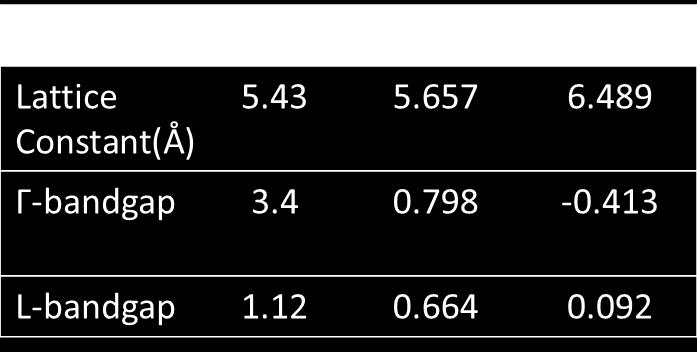
46 GeSn Material Challenges Very low solubility of Sn in Ge and Si (<1%) Hard to prevent Sn Segregation and precipitations Very large lattice mismatch a Si =5.431Å; a Ge =5.657Å; a Sn =6.489Å Low temperature growth


47 Experimental Effort NTU-UMass Boston Collaboration Low temperature MBE growth LED with highest Sn content: Ge Sn 0.078
48 Fabrication of p-i-n diode Etch Clean First Second Open Third Deposit down custom metal the SiO2 sample window n-layer mask Si cap P-type doped Ge Ge spacer Ni GeSn layer Ge spacer N-type doped Ge Ge buffer Si buffer Silicon substrate PR PR PR SiO2 PR SiO2 48
49 49
50 Next Step for GeSn Laser Diodes Mid-IR double heterostructure GeSn laser on Si substrate (low temperature) Mid-IR quantum well GeSn laser on Si substrate (room temperature) 50
51 The Group-IV Intersubband Approach Quantum cascade lasers Circumventing the band indirectness completely Mid-IR to THz range With advantages for being nonpolar material system Facing material challenges 51
52 Band-to-band Transitions in QWs ΔE c u In-plane k Subband ħω ħω ΔE v l In-plane k 1) Light emitters require direct band gap 2) Wavelength is determined by the band gap
53 Intersubband Transitions in QWs E 2 ΔE c ħω ħω E 1 In-plane k 1) Intersubband transition is always direct in k-space 2) Wavelength is determined by the subband separation, no longer by the bandgap.
54 Brief History First semiconductor laser demonstrated in 1962 Original idea of IST laser proposed in 1971 by Kazarinov and Suris First QCL based on IST in 1994 (Bell Labs) Why takes so long?
55 Band-to-band vs. Intersubband i u ħω ħω l g Lasers based on ISTs are far more complex than conventional lasers.
56 Band Engineering E 2 E 1 Separated QWs Coupled QWs QW width yields the subband level and separation Barrier width and height determine subband overlap


57 Optically Pumped IST Laser Barrier/QW active region Pumping light (TM polarized) n-type cladding layer n-type cladding buffer Lasing emission (TM polarized) Substrate
58 Optically Pumped IST Lasing Process p L p L Periodic coupled MQW structure (n-doped) Optical Pumping: 1 3; Lasing: 3 2 Depopulation: 2 1; Population inversion: 32 > 2

59 Electron Scattering Phonon absorption Subband 2 Subband 1 Intrasubband process Phonon emission Electron-phonon scattering electron- Electron scattering Electron-electron scattering

60 Optical Phonon Scattering γ 21 = 2π ħ 1 H ep H ep 2 2 δ E 2 E 1 ħω p dn G 12 Q 2 n p, Absorption G 12 Q 2 n p + 1, Emission absorption 2 1 Emission n p = 1 exp ħω p k B T 1 γ 21 [1/ps] ( 0. 1 for GeSn) E 2 E 1 /ħω p
61 Optical Phonon Emission u l u l g g Q ħω p ħω p ħω p IST above optical phonon Q IST below optical phonon
62
63 Population Analysis (Current Injection) N 3 t = ηj e N 3 N 3 τ 3 N 2 t = N 3 N 3 τ 32 N 2 N 2 τ 2 Population inversion: N 3 N 3 = τ 3 1 τ 2 τ 32 ηj e N 2 N 3 τ 32 > τ 2 Thermal backfilling

64 Current Injection IST Laser Metal contact n-type cladding contact layer V Barrier/QW active Region Metal contact n-type Cladding buffer Lasing n-type Substrate

65 Quantum Cascade Laser
66 Features and Advantages Unipolar (n-i-n or p-i-p ) device Fast modulation time Design freedom Lasing wavelength tunable by design: Mid to far-ir to THz range Bandgap directness irrelevant - favorable for Si-based lasers
67 History and Status 1992, first design of intersubband laser by G. Sun and J. B. Khurgin 1994, first QCL demonstration by Bell Labs Lasers based on III-V (GaAs, InGaAs, AlGaAs, InAlAs on GaAs or InP substrate) material systems Lasing wavelengths from 3μm to ~200μm CW, room temperature operation on selected wavelengths in InP based QCLs THz lasers bridging the gap between far-infrared coherent light source and GHz microwave electronics (100GHz ~ 10THz) operating below 200K
 2004: THz selected as one of 10 emerging technologies that will change your")
68 IST Bridging the THz gap For a long time there were no adequate sources operating in this range. Technology Review (MIT) 2004: THz selected as one of 10 emerging technologies that will change your world


69 THz security imaging Military IR countermeasures


70 THz medical imaging Clinical image THz image THz molecular sensing


71 Existing THz Sources Free electron lasers Molecular gas lasers THz Quantum Cascade Lasers

72 Circumventing the Indirect Bandgap E L-valleys in Ge or Ge-rich SiGe E Δ-valleys in Si or Si-rich SiGe CB Γ Δ or L-valley K Indirect K VB Band indirectness becomes irrelevant!
73 Si-based Intersubband Efforts Intersubband approach proposed in SiGe/Si QWs (G. Sun et al, 1995) Intersubband EL demonstrated in SiGe/Si Quantum cascade structures: G. Dehlinger et al (Switzerland, 2000) I. Bormann et al (Germany, 2002) S. A. Lynch et al (England, 2002) One scheme in common Intersubband transitions in valence band


74 SiGe Intersubband Devices Intersubband transitions within the valence band of GeSi/Si quantum Wells Metal Conduction Band p-sige cladding SiGe/Si QW active region p-sige buffer p-type Si substrate Lasing V Lasing Si barrier Eg Valence Band GeSi QW Si barrier SiGe quantum wells with Si barriers Small offset in conduction band Large offset in valence band p-i-p structure Electro-luminescence demonstrated but no lasing so far G. Sun, L. Friedman, and R. A. Soref, APL, vol.66, 3425 (1995)
75 Challenges and Opportunities Challenges: Unparallel valence subband dispersion due to light hole heavy hole coupling Difficulty in growing multiple QWs of large thickness due to large lattice mismatch (4%) between Si and Ge Low carrier transport and small oscillator strength due to large hole effective mass Opportunities: Lower threshold because of longer subband lifetimes due to weaker scattering of nonpolar optical phonons Strain and band offset engineering by incorporating yet another group-iv element Sn into the system
76 GeSiSn/Ge Strain Free QCLs Lattice matched structure no limitations on number of layers and thickness Large L-valley offset conduction band intersubband lasers
77 Ge/GeSiSn Conduction Band Offset Energy Calculation based on Jaros Band offset theory [Phys. Rev. B 37, 7112 (1988)] Conduction Γ, X, and L valleys for lattice matched GeSiSn alloy with Ge L-valleys for both GeSiSn and Ge below all others for Sn < 5% ΔE L =150meV between Ge well and Ge 0.76 Si 0.19 Sn 0.05 barrier

78 Ge/GeSiSn QCL on Si Substrate Growth of relaxed Ge layers directly on Si substrate Ge layers in 40nm -1µm thickness Edge dislocations formed at interface Low threading dislocation density < 10 5 /cm 2 Strain Free Ge/GeSiSn QCLs can be lattice matched to relaxed Ge buffer layer on Si substrate
79 L-Valley Ge/GeSiSn QCL L-valley CB offset: 150meV; Effective mass: 0.12m o ; Electric field: 10kV/cm Active region: 3 states with 3 QWs; lasing transition: 3 2 (49µm) Injector region: miniband formed with 4 QWs; upper state 3 in miniband gap; strong overlap between state 2 and miniband.
80 Lifetimes Carrier scattering due to nonpolar Optical and acoustic phonons Population inversion: 32 2
81 Population Dynamics and Optical Gain N i )] ( ) (1 [ 2 3 ) ( 2 3 _ 2 _ N N e J L n c z e g p o L 2 _ _ _ N N N N t N N N e J t N Population rate equation at threshold Current injection 3 2 Carrier scattering Depopulation Optical gain Dipole matrix overlap Lifetime requirement for inversion Thermal population
82 Plasmon Waveguide Conventional dielectric waveguides unsuitable for far-ir QCLs (d<<λ) Plasmon waveguides with metal cladding layers effective for mode confinement Only TM-polarized modes allowed Waveguide loss associated with metal absorption
83 Plasmon Waveguide Mode TM mode H y q( x ae bcosh( q( xd ae d /2) kx) e /2) e e j( zt ) j( zt ) j( zt ),,, x d / 2 x d / 2 x d / 2 M cosh( kd / 2) E ˆ ˆ o j q e e x d E E j kx xˆ k kx zˆ e x d cosh( kd / 2) E ˆ ˆ o j q e e x d q( xd /2) j( zt) ( x z), / 2 j( zt ) o[ cosh( ) sinh( ) ], / 2 M q( xd /2) j( zt ) ( x z), / 2 2 P 1 ' j" i 2
84 Plasmon Waveguide Confinement Electric field Profile: d /2 d /2 E E 2 2 dx dx Optical confinement Γ 1.0 Waveguide loss: α W =110/cm For d=2.1µm (40 periods of QCL)
85 QCL Threshold Current Optical Gain: g 2e 2 ( L ) 3 z cnl o p [ ( J ) e _ ( N 2 _ N 3 )] 1.0, m 10 / 110 / w cm cm 3 z nm Confinement factor Waveguide loss FWHM=10meV gth w m Mirror loss In comparison with GaAs-based QCLs, this represents a reduction in threshold current density!
86 SiGeSn Works from Other Groups Kasper s group, University of Stuttgart Harris group, Stanford University Kolodzey s group, University of Delaware Yu s group, University of Arkansas Imec and Catholic University of Leuven, Belgium Nagoya University, Japan
87 Summary Group-IV system (Si, Ge, Sn and their alloys) is being investigated for photonic devices on Si substrates Strain and bandgap engineering are being explored. Direct bandgap GeSn is within reach. Group-IV LEDs have been reported as well as IR detectors. Progress is being made, but there remain significant material challenges. GeSn laser diodes are expected in near future. GeSiSn QCL is more futuristic.
Optically-Pumped Ge-on-Si Gain Media: Lasing and Broader Impact
 Optically-Pumped Ge-on-Si Gain Media: Lasing and Broader Impact J. Liu 1, R. Camacho 2, X. Sun 2, J. Bessette 2, Y. Cai 2, X. X. Wang 1, L. C. Kimerling 2 and J. Michel 2 1 Thayer School, Dartmouth College;
InGaAs-AlAsSb quantum cascade lasers
 InGaAs-AlAsSb quantum cascade lasers D.G.Revin, L.R.Wilson, E.A.Zibik, R.P.Green, J.W.Cockburn Department of Physics and Astronomy, University of Sheffield, UK M.J.Steer, R.J.Airey EPSRC National Centre
Three-Dimensional Silicon-Germanium Nanostructures for Light Emitters and On-Chip Optical. Interconnects
 Three-Dimensional Silicon-Germanium Nanostructures for Light Emitters and On-Chip Optical eptember 2011 Interconnects Leonid Tsybeskov Department of Electrical and Computer Engineering New Jersey Institute
Ge Quantum Well Modulators on Si. D. A. B. Miller, R. K. Schaevitz, J. E. Roth, Shen Ren, and Onur Fidaner
 10.1149/1.2986844 The Electrochemical Society Ge Quantum Well Modulators on Si D. A. B. Miller, R. K. Schaevitz, J. E. Roth, Shen Ren, and Onur Fidaner Ginzton Laboratory, 450 Via Palou, Stanford CA 94305-4088,
Terahertz Lasers Based on Intersubband Transitions
 Terahertz Lasers Based on Intersubband Transitions Personnel B. Williams, H. Callebaut, S. Kumar, and Q. Hu, in collaboration with J. Reno Sponsorship NSF, ARO, AFOSR,and NASA Semiconductor quantum wells
High performance THz quantum cascade lasers
 High performance THz quantum cascade lasers Karl Unterrainer M. Kainz, S. Schönhuber, C. Deutsch, D. Bachmann, J. Darmo, H. Detz, A.M. Andrews, W. Schrenk, G. Strasser THz QCL performance High output power
3-1-2 GaSb Quantum Cascade Laser
 3-1-2 GaSb Quantum Cascade Laser A terahertz quantum cascade laser (THz-QCL) using a resonant longitudinal optical (LO) phonon depopulation scheme was successfully demonstrated from a GaSb/AlSb material
Intraband emission of GaN quantum dots at λ =1.5 μm via resonant Raman scattering
 Intraband emission of GaN quantum dots at λ =1.5 μm via resonant Raman scattering L. Nevou, F. H. Julien, M. Tchernycheva, J. Mangeney Institut d Electronique Fondamentale, UMR CNRS 8622, University Paris-Sud
Emission Spectra of the typical DH laser
 Emission Spectra of the typical DH laser Emission spectra of a perfect laser above the threshold, the laser may approach near-perfect monochromatic emission with a spectra width in the order of 1 to 10
Laser Diodes. Revised: 3/14/14 14: , Henry Zmuda Set 6a Laser Diodes 1
 Laser Diodes Revised: 3/14/14 14:03 2014, Henry Zmuda Set 6a Laser Diodes 1 Semiconductor Lasers The simplest laser of all. 2014, Henry Zmuda Set 6a Laser Diodes 2 Semiconductor Lasers 1. Homojunction
Lecture 2. Electron states and optical properties of semiconductor nanostructures
 Lecture Electron states and optical properties of semiconductor nanostructures Bulk semiconductors Band gap E g Band-gap slavery: only light with photon energy equal to band gap can be generated. Very
Chapter 5. Semiconductor Laser
 Chapter 5 Semiconductor Laser 5.0 Introduction Laser is an acronym for light amplification by stimulated emission of radiation. Albert Einstein in 1917 showed that the process of stimulated emission must
OPTI510R: Photonics. Khanh Kieu College of Optical Sciences, University of Arizona Meinel building R.626
 OPTI510R: Photonics Khanh Kieu College of Optical Sciences, University of Arizona kkieu@optics.arizona.edu Meinel building R.626 Announcements HW #6 is assigned, due April 23 rd Final exam May 2 Semiconductor
THz SOURCES BASED ON INTERSUBBAND TRANSITIONS IN QUANTUM WELLS AND STRAINED LAYERS *
 Fourth International Symposium on Space Terahertz Technology Page 573 THz SOURCES BASED ON INTERSUBBAND TRANSITIONS IN QUANTUM WELLS AND STRAINED LAYERS * A. Afzali-Kushaa, G. I. Haddad, and T. B. Norris
Short wavelength and strain compensated InGaAs-AlAsSb. AlAsSb quantum cascade lasers. D.Revin, S.Zhang, J.Cockburn, L.Wilson, S.
 Short wavelength and strain compensated InGaAs-AlAsSb AlAsSb quantum cascade lasers D.Revin, S.Zhang, J.Cockburn, L.Wilson, S.Menzel, Department of Physics and Astronomy, University of Sheffield, United
Electronic Materials, Heterostrucuture Semiconductor, Light Emitting Devices, Molecular Beam Epitaxy
 REPORT DOCUMENTATION PAGE Form Approved OMB No. 0704-0188 The public reporting burden for this collection of information is estimated to average 1 hour per response, including the time for reviewing instructions,
GeSi Quantum Dot Superlattices
 GeSi Quantum Dot Superlattices ECE440 Nanoelectronics Zheng Yang Department of Electrical & Computer Engineering University of Illinois at Chicago Nanostructures & Dimensionality Bulk Quantum Walls Quantum
MONTE CARLO SIMULATION OF ELECTRON DYNAMICS IN QUANTUM CASCADE LASERS. Xujiao Gao
 MONTE CARLO SIMULATION OF ELECTRON DYNAMICS IN QUANTUM CASCADE LASERS by Xujiao Gao A dissertation submitted in partial fulfillment of the requirements for the degree of Doctor of Philosophy (Electrical
White Rose Research Online URL for this paper:
 This is a repository copy of Self-consistent solutions to the intersubband rate equations in quantum cascade lasers: Analysis of a GaAs/AlxGa1-xAs device. White Rose Research Online URL for this paper:
Pressure and Temperature Dependence of Threshold Current in Semiconductor Lasers Based on InGaAs/GaAs Quantum-Well Systems
 Vol. 112 (2007) ACTA PHYSICA POLONICA A No. 2 Proceedings of the XXXVI International School of Semiconducting Compounds, Jaszowiec 2007 Pressure and Temperature Dependence of Threshold Current in Semiconductor
Practical Quantum-Dot Lasers Monolithically Grown on Silicon for Silicon Photonics
 Department of Electronic and Electrical Engineering London Centre for Nanotechnology Practical Quantum-Dot Lasers Monolithically Grown on Silicon for Silicon Photonics Huiyun Liu Outline Why lasers on
Thermal and electronic analysis of GaInAs/AlInAs mid-ir
 Thermal and electronic analysis of GaInAs/AlInAs mid-ir QCLs Gaetano Scamarcio Miriam S. Vitiello, Vincenzo Spagnolo, Antonia Lops oratory LIT 3, CNR - INFM Physics Dept.,University of Bari, Italy T. Gresch,
interband transitions in semiconductors M. Fox, Optical Properties of Solids, Oxford Master Series in Condensed Matter Physics
 interband transitions in semiconductors M. Fox, Optical Properties of Solids, Oxford Master Series in Condensed Matter Physics interband transitions in quantum wells Atomic wavefunction of carriers in
Nonlinear optics with quantum-engineered intersubband metamaterials
 Nonlinear optics with quantum-engineered intersubband metamaterials Mikhail Belkin Department of Electrical and Computer Engineering The University of Texas at Austin 1 Mid-infrared and THz photonics Electronics
Self-Assembled InAs Quantum Dots
 Self-Assembled InAs Quantum Dots Steve Lyon Department of Electrical Engineering What are semiconductors What are semiconductor quantum dots How do we make (grow) InAs dots What are some of the properties
Introduction to Optoelectronic Device Simulation by Joachim Piprek
 NUSOD 5 Tutorial MA Introduction to Optoelectronic Device Simulation by Joachim Piprek Outline:. Introduction: VCSEL Example. Electron Energy Bands 3. Drift-Diffusion Model 4. Thermal Model 5. Gain/Absorption
OPTI510R: Photonics. Khanh Kieu College of Optical Sciences, University of Arizona Meinel building R.626
 OPTI510R: Photonics Khanh Kieu College of Optical Sciences, University of Arizona kkieu@optics.arizona.edu Meinel building R.626 Announcements HW#3 is assigned due Feb. 20 st Mid-term exam Feb 27, 2PM
Luminescence basics. Slide # 1
 Luminescence basics Types of luminescence Cathodoluminescence: Luminescence due to recombination of EHPs created by energetic electrons. Example: CL mapping system Photoluminescence: Luminescence due to
Optical Nonlinearities in Quantum Wells
 Harald Schneider Institute of Ion-Beam Physics and Materials Research Semiconductor Spectroscopy Division Rosencher s Optoelectronic Day Onéra 4.05.011 Optical Nonlinearities in Quantum Wells Harald Schneider
Luminescence Process
 Luminescence Process The absorption and the emission are related to each other and they are described by two terms which are complex conjugate of each other in the interaction Hamiltonian (H er ). In an
3-1-1 GaAs-based Quantum Cascade Lasers
 3 Devices 3-1 Oscillator 3-1-1 GaAs-based Quantum Cascade Lasers Quantum cascade lasers (QCLs) have different structures and characteristics from those of conventional semiconductor lasers commonly used
Nanophysics: Main trends
 Nano-opto-electronics Nanophysics: Main trends Nanomechanics Main issues Light interaction with small structures Molecules Nanoparticles (semiconductor and metallic) Microparticles Photonic crystals Nanoplasmonics
(b) Spontaneous emission. Absorption, spontaneous (random photon) emission and stimulated emission.
 Spontaneous emission. Absorption, spontaneous (random photon) emission and stimulated emission.") Lecture 10 Stimulated Emission Devices Lasers Stimulated emission and light amplification Einstein coefficients Optical fiber amplifiers Gas laser and He-Ne Laser The output spectrum of a gas laser Laser
Lecture 10 Stimulated Emission Devices Lasers Stimulated emission and light amplification Einstein coefficients Optical fiber amplifiers Gas laser and He-Ne Laser The output spectrum of a gas laser Laser
Widely Tunable and Intense Mid-Infrared PL Emission from Epitaxial Pb(Sr)Te Quantum Dots in a CdTe Matrix
Te Quantum Dots in a CdTe Matrix") Widely Tunable and Intense Mid-Infrared PL Emission from Epitaxial Pb(Sr)Te Quantum Dots in a Matrix S. Kriechbaumer 1, T. Schwarzl 1, H. Groiss 1, W. Heiss 1, F. Schäffler 1,T. Wojtowicz 2, K. Koike 3,
Widely Tunable and Intense Mid-Infrared PL Emission from Epitaxial Pb(Sr)Te Quantum Dots in a Matrix S. Kriechbaumer 1, T. Schwarzl 1, H. Groiss 1, W. Heiss 1, F. Schäffler 1,T. Wojtowicz 2, K. Koike 3,
Physics and Material Science of Semiconductor Nanostructures
 Physics and Material Science of Semiconductor Nanostructures PHYS 570P Prof. Oana Malis Email: omalis@purdue.edu Course website: http://www.physics.purdue.edu/academic_programs/courses/phys570p/ 1 Course
Metal Vapour Lasers Use vapoured metal as a gain medium Developed by W. Silfvast (1966) Two types: Ionized Metal vapour (He-Cd) Neutral Metal vapour
 Two types: Ionized Metal vapour (He-Cd) Neutral Metal vapour") Metal Vapour Lasers Use vapoured metal as a gain medium Developed by W. Silfvast (1966) Two types: Ionized Metal vapour (He-Cd) Neutral Metal vapour (Cu) All operate by vaporizing metal in container Helium
Metal Vapour Lasers Use vapoured metal as a gain medium Developed by W. Silfvast (1966) Two types: Ionized Metal vapour (He-Cd) Neutral Metal vapour (Cu) All operate by vaporizing metal in container Helium
Infrared Quantum Cascade Laser
 Infrared Quantum Cascade Laser W. Schrenk, N. Finger, S. Gianordoli, L. Hvozdara, E. Gornik, and G. Strasser Institut für Festkörperelektronik, Technische Universität Wien Floragasse 7, 1040 Wien, Austria
Heterostructures and sub-bands
 Heterostructures and sub-bands (Read Datta 6.1, 6.2; Davies 4.1-4.5) Quantum Wells In a quantum well, electrons are confined in one of three dimensions to exist within a region of length L z. If the barriers
InAs/GaSb Mid-Wave Cascaded Superlattice Light Emitting Diodes
 InAs/GaSb Mid-Wave Cascaded Superlattice Light Emitting Diodes John Prineas Department of Physics and Astronomy, University of Iowa May 3, 206 Collaborator: Thomas Boggess Grad Students: Yigit Aytak Cassandra
Electromagnetically Induced Transparency (EIT) via Spin Coherences in Semiconductor
 via Spin Coherences in Semiconductor") Electromagnetically Induced Transparency (EIT) via Spin Coherences in Semiconductor Hailin Wang Oregon Center for Optics, University of Oregon, USA Students: Shannon O Leary Susanta Sarkar Yumin Shen Phedon
Electromagnetically Induced Transparency (EIT) via Spin Coherences in Semiconductor Hailin Wang Oregon Center for Optics, University of Oregon, USA Students: Shannon O Leary Susanta Sarkar Yumin Shen Phedon
Oscillateur paramétrique optique en
 C. Ozanam 1, X. Lafosse 2, I. Favero 1, S. Ducci 1, G. Leo 1 1 Université Paris Diderot, Sorbonne Paris Cité, Laboratoire MPQ, CNRS-UMR 7162, Paris, France, 2 Laboratoire de Photonique et Nanostructures,
Thermal performance investigation of DQW GaInNAs laser diodes
 Thermal performance investigation of DQW GaInNAs laser diodes Jun Jun Lim, Roderick MacKenzie, Slawomir Sujecki, Eric Larkins Photonic and Radio Frequency Engineering Group, School of Electrical and Electronic
Resonator Fabrication for Cavity Enhanced, Tunable Si/Ge Quantum Cascade Detectors
 Resonator Fabrication for Cavity Enhanced, Tunable Si/Ge Quantum Cascade Detectors M. Grydlik 1, P. Rauter 1, T. Fromherz 1, G. Bauer 1, L. Diehl 2, C. Falub 2, G. Dehlinger 2, H. Sigg 2, D. Grützmacher
THz QCL sources based on intracavity difference-frequency mixing
 THz QCL sources based on intracavity difference-frequency mixing Mikhail Belkin Department of Electrical and Computer Engineering The University of Texas at Austin IQCLSW, Sept. 3, 218 Problems with traditional
Photodetector. Prof. Woo-Young Choi. Silicon Photonics (2012/2) Photodetection: Absorption => Current Generation. Currents
 Photodetection: Absorption => Current Generation. Currents") Photodetection: Absorption => Current Generation h Currents Materials for photodetection: E g < h Various methods for generating currents with photo-generated carriers: photoconductors, photodiodes, avalanche
Photodetection: Absorption => Current Generation h Currents Materials for photodetection: E g < h Various methods for generating currents with photo-generated carriers: photoconductors, photodiodes, avalanche
Simple strategy for enhancing terahertz emission from coherent longitudinal optical phonons using undoped GaAs/n-type GaAs epitaxial layer structures
 Presented at ISCS21 June 4, 21 Session # FrP3 Simple strategy for enhancing terahertz emission from coherent longitudinal optical phonons using undoped GaAs/n-type GaAs epitaxial layer structures Hideo
Carrier Dynamics in Quantum Cascade Lasers
 Vol. 107 (2005) ACTA PHYSICA POLONICA A No. 1 Proceedings of the 12th International Symposium UFPS, Vilnius, Lithuania 2004 Carrier Dynamics in Quantum Cascade Lasers P. Harrison a, D. Indjin a, V.D. Jovanović
ISSN Review. Progress to a Gallium-Arsenide Deep-Center Laser
 Materials 2009, 2, 1599-1635; doi:10.3390/ma2041599 OPEN ACCESS materials ISSN 1996-1944 www.mdpi.com/journal/materials Review Progress to a Gallium-Arsenide Deep-Center Laser Janet L. Pan Yale University,
Signal regeneration - optical amplifiers
 Signal regeneration - optical amplifiers In any atom or solid, the state of the electrons can change by: 1) Stimulated absorption - in the presence of a light wave, a photon is absorbed, the electron is
Optical Investigation of the Localization Effect in the Quantum Well Structures
 Department of Physics Shahrood University of Technology Optical Investigation of the Localization Effect in the Quantum Well Structures Hamid Haratizadeh hamid.haratizadeh@gmail.com IPM, SCHOOL OF PHYSICS,
Chapter 4. Photodetectors
 Chapter 4 Photodetectors Types of photodetectors: Photoconductos Photovoltaic Photodiodes Avalanche photodiodes (APDs) Resonant-cavity photodiodes MSM detectors In telecom we mainly use PINs and APDs.
Electroluminescence from Silicon and Germanium Nanostructures
 Electroluminescence from silicon Silicon Getnet M. and Ghoshal S.K 35 ORIGINAL ARTICLE Electroluminescence from Silicon and Germanium Nanostructures Getnet Melese* and Ghoshal S. K.** Abstract Silicon
Stimulated Emission Devices: LASERS
 Stimulated Emission Devices: LASERS 1. Stimulated Emission and Photon Amplification E 2 E 2 E 2 hυ hυ hυ In hυ Out hυ E 1 E 1 E 1 (a) Absorption (b) Spontaneous emission (c) Stimulated emission The Principle
Electronic and Optoelectronic Properties of Semiconductor Structures
 Electronic and Optoelectronic Properties of Semiconductor Structures Jasprit Singh University of Michigan, Ann Arbor CAMBRIDGE UNIVERSITY PRESS CONTENTS PREFACE INTRODUCTION xiii xiv 1.1 SURVEY OF ADVANCES
Electron Energy, E E = 0. Free electron. 3s Band 2p Band Overlapping energy bands. 3p 3s 2p 2s. 2s Band. Electrons. 1s ATOM SOLID.
 Electron Energy, E Free electron Vacuum level 3p 3s 2p 2s 2s Band 3s Band 2p Band Overlapping energy bands Electrons E = 0 1s ATOM 1s SOLID In a metal the various energy bands overlap to give a single
MODAL GAIN AND CURRENT DENSITY RELATIONSHIP FOR PbSe/PbSrSe QUANTUM WELL NORMAL AND OBLIQUE DEGENERATE VALLEYS
 Far East Journal of Electronics and Communications 17 Pushpa Publishing House, Allahabad, India http://www.pphmj.com http://dx.doi.org/1.17654/ec1761319 Volume 17, Number 6, 17, Pages 1319-136 ISSN: 973-76
School of Electrical and Computer Engineering, Cornell University. ECE 5330: Semiconductor Optoelectronics. Fall 2014
 School of Electrical and Computer Engineering, Cornell University ECE 5330: Semiconductor Optoelectronics Fall 014 Homework 7 Due on Nov. 06, 014 Suggested Readings: i) Study lecture notes. ii) Study Coldren
Laser Basics. What happens when light (or photon) interact with a matter? Assume photon energy is compatible with energy transition levels.
 interact with a matter? Assume photon energy is compatible with energy transition levels.") What happens when light (or photon) interact with a matter? Assume photon energy is compatible with energy transition levels. Electron energy levels in an hydrogen atom n=5 n=4 - + n=3 n=2 13.6 = [ev]
What happens when light (or photon) interact with a matter? Assume photon energy is compatible with energy transition levels. Electron energy levels in an hydrogen atom n=5 n=4 - + n=3 n=2 13.6 = [ev]
Fabrication of Efficient Blue Light-Emitting Diodes with InGaN/GaN Triangular Multiple Quantum Wells. Abstract
 Fabrication of Efficient Blue Light-Emitting Diodes with InGaN/GaN Triangular Multiple Quantum Wells R. J. Choi, H. W. Shim 2, E. K. Suh 2, H. J. Lee 2, and Y. B. Hahn,2, *. School of Chemical Engineering
1. Binary III-V compounds 2 p From which atoms are the 16 binary III-V compounds formed?...column III B, Al, Ga and In...column V N, P, As and Sb...
 PROBLEMS part B, Semiconductor Materials. 2006 1. Binary III-V compounds 2 p From which atoms are the 16 binary III-V compounds formed?...column III B, Al, Ga and In...column V N, P, As and Sb... 2. Semiconductors
Temperature Dependent Optical Band Gap Measurements of III-V films by Low Temperature Photoluminescence Spectroscopy
 Temperature Dependent Optical Band Gap Measurements of III-V films by Low Temperature Photoluminescence Spectroscopy Linda M. Casson, Francis Ndi and Eric Teboul HORIBA Scientific, 3880 Park Avenue, Edison,
Far-infrared optical properties of. Ge/SiGe quantum well systems. Diego Sabbagh
 Università degli Studi Roma Tre Dipartimento di Matematica e Fisica Far-infrared optical properties of Ge/SiGe quantum well systems Diego Sabbagh in partial fulfillment of the requirements for the degree
Semiconductors and Optoelectronics. Today Semiconductors Acoustics. Tomorrow Come to CH325 Exercises Tours
 Semiconductors and Optoelectronics Advanced Physics Lab, PHYS 3600 Don Heiman, Northeastern University, 2017 Today Semiconductors Acoustics Tomorrow Come to CH325 Exercises Tours Semiconductors and Optoelectronics
Semiconductor Quantum Dot Nanostructures and their Roles in the Future of Photonics
 550 Brazilian Journal of Physics, vol. 34, no. 2B, June, 2004 Semiconductor Quantum Dot Nanostructures and their Roles in the Future of Photonics S. Fafard, K. Hinzer, and C. N. Allen Institute for Microstructural
Optoelectronics ELEC-E3210
 Optoelectronics ELEC-E3210 Lecture 3 Spring 2017 Semiconductor lasers I Outline 1 Introduction 2 The Fabry-Pérot laser 3 Transparency and threshold current 4 Heterostructure laser 5 Power output and linewidth
Photonics applications II. Ion-doped ChGs
 Photonics applications II Ion-doped ChGs 1 ChG as a host for doping; pros and cons - Important - Condensed summary Low phonon energy; Enabling emission at longer wavelengths Reduced nonradiative multiphonon
ON THE POSSIBILITY OF AN INTERSUBBAND LASER IN SILICON-ON-INSULATOR
 International Journal of High Speed Electronics and Systems Vol. 16, No 2 (2006) pp. 411-420 World Scientific Publishing Company ON THE POSSIBILITY OF AN INTERSUBBAND LASER IN SILICON-ON-INSULATOR SERGE
ρ ρ LED access resistances d A W d s n s p p p W the output window size p-layer d p series access resistance d n n-layer series access resistance
 LED access resistances W the output window size p-layer series access resistance d p n-layer series access resistance d n The n-layer series access resistance R = ρ s n where the resistivity of the n-layer
Segmented 1.55um Laser with 400% Differential Quantum Efficiency J. Getty, E. Skogen, L. Coldren, University of California, Santa Barbara, CA.
 Segmented 1.55um Laser with 400% Differential Quantum Efficiency J. Getty, E. Skogen, L. Coldren, University of California, Santa Barbara, CA. Abstract: By electrically segmenting, and series-connecting
Quantum Dot Lasers. Andrea Fiore. Ecole Polytechnique Fédérale de Lausanne
 Quantum Dot Lasers Ecole Polytechnique Fédérale de Lausanne Outline: Quantum-confined active regions Self-assembled quantum dots Laser applications Electronic states in semiconductors Schrödinger eq.:
Quantum and Non-local Transport Models in Crosslight Device Simulators. Copyright 2008 Crosslight Software Inc.
 Quantum and Non-local Transport Models in Crosslight Device Simulators Copyright 2008 Crosslight Software Inc. 1 Introduction Quantization effects Content Self-consistent charge-potential profile. Space
Semiconductor Lasers II
 Semiconductor Lasers II Materials and Structures Edited by Eli Kapon Institute of Micro and Optoelectronics Department of Physics Swiss Federal Institute oftechnology, Lausanne OPTICS AND PHOTONICS ACADEMIC
High Power Diode Lasers
 Lecture 10/1 High Power Diode Lasers Low Power Lasers (below tenth of mw) - Laser as a telecom transmitter; - Laser as a spectroscopic sensor; - Laser as a medical diagnostic tool; - Laser as a write-read
Quantum cascade lasers at 16 µm wavelength based on GaAs/AlGaAs
 Quantum cascade lasers at 16 µm wavelength based on GaAs/AlGaAs Sara Anjum January 9, 2018 Advised by: Claire Gmachl This paper represents my own work in accordance with University regulations. /s/ Sara
Quantum-cascade lasers without injector regions
 Invited Paper Quantum-cascade lasers without injector regions A. Friedrich* and M.-C. Amann Walter Schottky Institute, Technical University of Munich, D-878 Garching, Germany ABSTRACT We present the status
Semiconductor Lasers for Optical Communication
 Semiconductor Lasers for Optical Communication Claudio Coriasso Manager claudio.coriasso@avagotech.com Turin Technology Centre 10Gb/s DFB Laser MQW 1 Outline 1) Background and Motivation Communication
Ultrafast carrier dynamics in InGaN MQW laser diode
 Invited Paper Ultrafast carrier dynamics in InGaN MQW laser diode Kian-Giap Gan* a, Chi-Kuang Sun b, John E. Bowers a, and Steven P. DenBaars a a Department of Electrical and Computer Engineering, University
Self-Consistent Treatment of V-Groove Quantum Wire Band Structure in Nonparabolic Approximation
 SERBIAN JOURNAL OF ELECTRICAL ENGINEERING Vol. 1, No. 3, November 2004, 69-77 Self-Consistent Treatment of V-Groove Quantum Wire Band Structure in Nonparabolic Approximation Jasna V. Crnjanski 1, Dejan
Theoretical investigation on intrinsic linewidth of quantum cascade lasers. Liu Tao
 Theoretical investigation on intrinsic linewidth of quantum cascade lasers Liu Tao School of Electrical and Electronic Engineering 014 Theoretical investigation on intrinsic linewidth of quantum cascade
40. Quantum Wells, Superlattices, and Band-Gap Engineering
 1037 40. Quantum Wells, Superlattices, We and Band-Gap Engineering Mark Fox, Radu Ispasoiu This chapter reviews the principles of bandgap engineering and quantum confinement in semiconductors, with a particular
Simulation of Quantum Cascade Lasers
 Lighting up the Semiconductor World Simulation of Quantum Cascade Lasers 2005-2010 Crosslight Software Inc. Lighting up the Semiconductor World A A Contents Microscopic rate equation approach Challenge
Semiconductor device structures are traditionally divided into homojunction devices
 0. Introduction: Semiconductor device structures are traditionally divided into homojunction devices (devices consisting of only one type of semiconductor material) and heterojunction devices (consisting
Photoluminescence characterization of quantum dot laser epitaxy
 Photoluminescence characterization of quantum dot laser epitaxy Y. Li *, Y. C. Xin, H. Su and L. F. Lester Center for High Technology Materials, University of New Mexico 1313 Goddard SE, Albuquerque, NM
1 Semiconductor Quantum Dots for Ultrafast Optoelectronics
 j1 1 Semiconductor Quantum Dots for Ultrafast Optoelectronics 1.1 The Role of Dimensionality in Semiconductor Materials The history of semiconductor lasers has been punctuated by dramatic revolutions.
THE terahertz (THz) region ( THz) of the electromagnetic
 region ( THz) of the electromagnetic") 952 IEEE JOURNAL OF SELECTED TOPICS IN QUANTUM ELECTRONICS, VOL. 15, NO. 3, MAY/JUNE 2009 High-Temperature Operation of Terahertz Quantum Cascade Laser Sources Mikhail A. Belkin, Member, IEEE, Qi Jie Wang,
952 IEEE JOURNAL OF SELECTED TOPICS IN QUANTUM ELECTRONICS, VOL. 15, NO. 3, MAY/JUNE 2009 High-Temperature Operation of Terahertz Quantum Cascade Laser Sources Mikhail A. Belkin, Member, IEEE, Qi Jie Wang,
Lasers. Stimulated Emission Lasers: Trapping Photons Terahertz Lasers Course Overview
 Lasers Stimulated Emission Lasers: Trapping Photons Terahertz Lasers Course Overview 1 P-N Junctions and LEDs Terminal Pins Emitted Light Beams Diode Transparent Plastic Case High energy electrons (n-type)
School of Electrical and Computer Engineering, Cornell University. ECE 5330: Semiconductor Optoelectronics. Fall Due on Nov 20, 2014 by 5:00 PM
 School of Electrical and Computer Engineering, Cornell University ECE 533: Semiconductor Optoelectronics Fall 14 Homewor 8 Due on Nov, 14 by 5: PM This is a long -wee homewor (start early). It will count
Designing a high speed 1310nm AlGaInAs/AlGaInAs VCSEL using MgO/Si top DBR and GaInAsP/InP bottom DBR
 American Journal of Optics and Photonics 014; (3): 37-44 Published online July 0, 014 (http://www.sciencepublishinggroup.com/j/ajop) doi: 10.11648/j.ajop.014003.14 ISSN: 330-8486 (Print); ISSN: 330-8494
NONLINEAR TRANSITIONS IN SINGLE, DOUBLE, AND TRIPLE δ-doped GaAs STRUCTURES
 NONLINEAR TRANSITIONS IN SINGLE, DOUBLE, AND TRIPLE δ-doped GaAs STRUCTURES E. OZTURK Cumhuriyet University, Faculty of Science, Physics Department, 58140 Sivas-Turkey E-mail: eozturk@cumhuriyet.edu.tr
3.46 PHOTONIC MATERIALS AND DEVICES Lecture 15: III-V Processing
 3.46 PHOTONIC MATERIALS AND DEVICES 15: III-V Processing Double Hetero structure laser (band structure engineering) AlGaAs GaAs AlGaAs e - E n hν P h + X n x I d < 1 μm 1. Large refractive index active
Room-temperature continuous-wave operation of GaInNAs/GaAs quantum dot laser with GaAsN barrier grown by solid source molecular beam epitaxy
 Room-temperature continuous-wave operation of GaInNAs/GaAs quantum dot laser with GaAsN barrier grown by solid source molecular beam epitaxy Z. Z. Sun 1, S. F. Yoon 1,2, K. C. Yew 1, and B. X. Bo 1 1 School
Carrier Loss Analysis for Ultraviolet Light-Emitting Diodes
 Carrier Loss Analysis for Ultraviolet Light-Emitting Diodes Joachim Piprek, Thomas Katona, Stacia Keller, Steve DenBaars, and Shuji Nakamura Solid State Lighting and Display Center University of California
Study on Quantum Dot Lasers and their advantages
 Study on Quantum Dot Lasers and their advantages Tae Woo Kim Electrical and Computer Engineering University of Illinois, Urbana Champaign Abstract Basic ideas for understanding a Quantum Dot Laser were
GaN-based Devices: Physics and Simulation
 GaN-based Devices: Physics and Simulation Joachim Piprek NUSOD Institute Collaborators Prof. Shuji Nakamura, UCSB Prof. Steve DenBaars, UCSB Dr. Stacia Keller, UCSB Dr. Tom Katona, now at S-ET Inc. Dr.
Novel materials and nanostructures for advanced optoelectronics
 Novel materials and nanostructures for advanced optoelectronics Q. Zhuang, P. Carrington, M. Hayne, A Krier Physics Department, Lancaster University, UK u Brief introduction to Outline Lancaster University
Nanoscience galore: hybrid and nanoscale photonics
 Nanoscience galore: hybrid and nanoscale photonics Pavlos Lagoudakis SOLAB, 11 June 2013 Hybrid nanophotonics Nanostructures: light harvesting and light emitting devices 2 Hybrid nanophotonics Nanostructures:
SUPPLEMENTARY INFORMATION
 doi:10.1038/nature12036 We provide in the following additional experimental data and details on our demonstration of an electrically pumped exciton-polariton laser by supplementing optical and electrical
Si - Based Tunnel Diode Operation and Forecasted Performance
 Si - Based Tunnel Diode Operation and Forecasted Performance Roger Lake Raytheon Systems Dallas, TX Si / Si x Ge -x Interband Tunnel Diodes The main tunneling process is LA and TO phonon assisted tunneling
The Report of the Characteristics of Semiconductor Laser Experiment
 The Report of the Characteristics of Semiconductor Laser Experiment Masruri Masruri (186520) 22/05/2008 1 Laboratory Setup The experiment consists of two kind of tasks: To measure the caracteristics of
Near-Infrared Spectroscopy of Nitride Heterostructures EMILY FINAN ADVISOR: DR. OANA MALIS PURDUE UNIVERSITY REU PROGRAM AUGUST 2, 2012
 Near-Infrared Spectroscopy of Nitride Heterostructures EMILY FINAN ADVISOR: DR. OANA MALIS PURDUE UNIVERSITY REU PROGRAM AUGUST 2, 2012 Introduction Experimental Condensed Matter Research Study of large