Chapter 9: Photovoltaic Devices
|
|
|
- Edith O’Neal’
- 5 years ago
- Views:
Transcription
1 Chapter 9: Photovoltaic Devices Solar energy spectrum Photovoltaic device principles pn junction photovoltaic I-V characteristics Series and shunt resistance Temperature effects Solar cell materials, devices, and efficiencies Current solar cell research PHYS5320 Chapter Nine 1
2 Photovoltaic devices or solar cells convert incident solar radiation energy into electrical energy. Incident photons are absorbed to photogenerate charge carriers that pass through an external load to do electrical work. Photovoltaic device applications range from calculators (~mw) to power plants (~MW). PHYS5320 Chapter Nine 2


3 Why Solar Energy? Clean Nearly unlimited Sunlight striking the earth in 1 hour: J All energy consumed on the earth recently per year: J PHYS5320 Chapter Nine 3


4 Solar cell plant PHYS5320 Chapter Nine 4


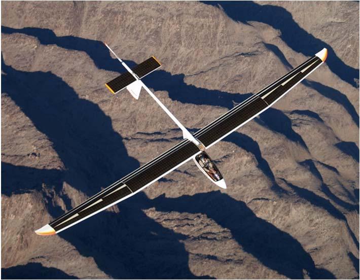
5 Cars and airplanes powered by photovoltaic devices PHYS5320 Chapter Nine 5

6 Solar Energy Spectrum Solar energy spectrum is typically represented by power per unit area per unit wavelength. The integrated intensity above Earth s atmosphere gives the total power flow through a unit area perpendicular to the direction of the sun. This quantity is called the air-mass zero (AM0) radiation and it is approximately constant at a value of kw m 2. PHYS5320 Chapter Nine 6
.")
7 Solar Energy Spectrum The actual intensity spectrum on Earth s surface depends on the absorption and scattering effects of the atmosphere, which increase with the sun beam s path through the atmosphere. The shortest path through the atmosphere is when the sun is directly above the location and the received spectrum is called air mass one (AM1). Air mass m is defined as the ratio of the actual radiation path to the shortest path. AMm = AM(1/cos). PV devices can be tilted to face the sun and maximize the collection efficiency. The terrestrial light has a diffuse component (due to scattering) in addition to the direct component. PHYS5320 Chapter Nine 7


8 Photovoltaic Device Principles short λ The heavily doped n-region is very narrow and most photons are absorbed in the depletion region and within the neutral p-side. EHPs generated in the depletion region are immediately separated by the built-in field. The electrons drift to the n-side and the holes drift to the p-side. PHYS5320 Chapter Nine 8

9 Photovoltaic Device Principles Finger electrodes on the n-side to allow illumination to enter the device. Anti-reflection coating. An open circuit voltage is established with the p-side positive with respect to the n-side. The photogenerated electrons in the neutral p-region will diffuse into the depletion region and drift to the n-side only if they are within the minority carrier diffusion length L e to the depletion region. Otherwise, they will recombine with the holes and get lost. The photogenerated holes in the neutral n-region within the minority carrier diffusion length L h to the depletion region will also probably contribute the photovoltaic effect. PHYS5320 Chapter Nine 9
 High-energy photons are absorbed near the crystal surface and get lost by the recombination in the surface region (~40%). (3) Reflection loss (~1020%).")
10 Photovoltaic Device Principles Losses for PV devices made of silicon: (1) Bandgap energy ~1.1 m. Incident photons with wavelengths larger than 1.1 m are wasted (~25%). (2) High-energy photons are absorbed near the crystal surface and get lost by the recombination in the surface region (~40%). (3) Reflection loss (~1020%). The upper limit to the efficiency of single-crystalline silicon PV cells is 2426% at room temperature. PHYS5320 Chapter Nine 10
11 Chapter 9: Photovoltaic Devices Solar energy spectrum Photovoltaic device principles pn junction photovoltaic I-V characteristics Series and shunt resistance Temperature effects Solar cell materials, devices, and efficiencies Current solar cell research PHYS5320 Chapter Nine 11

12 pn Junction Photovoltaic I-V Characteristics Consider a pn junction PV cell. The current and voltage in the figure follow the conventional definition of positive current and positive voltage for pn junctions. The photocurrent I ph is proportional to the light intensity I. The current in the case of a short circuit is I sc : I sc I ph KI PHYS5320 Chapter Nine 12
13 pn Junction Photovoltaic I-V Characteristics A current passing through a load resistor will generate a forward bias voltage on the pn junction. There will be a forward diode current. I d ev I 0 exp 1 nkbt I ev I ph Io exp 1 nkbt I V R PHYS5320 Chapter Nine 13
14 pn Junction Photovoltaic I-V Characteristics The power delivered to the load is P out = IV, which is the rectangle shown by the dashed lines in the figure. Maximum power is delivered to the load when the rectangular area is maximized (by changing R or the intensity of illumination). The fill factor is defined as FF IV I sc V max oc PHYS5320 Chapter Nine 14
15 Limiting Factors on V oc ev OC E g 1 T T sun kt ln emit sun ln 4n I 2 ln QE The first term arises from fundamental thermodynamic losses based on Carnot s theorem. The terms in the square brackets account for three entropyrelated contributions: 1st: entropy increase caused by photon absorption and reradiation; 2nd: the effect of incomplete light trapping. 3rd: the loss owing to non-radiative exciton recombination. A. Polman, H. A. Atwater, Nat. Mater. 2012, 11, 174. PHYS5320 Chapter Nine 15
16 Chapter 9: Photovoltaic Devices Solar energy spectrum Photovoltaic device principles pn junction photovoltaic I-V characteristics Series and shunt resistance Temperature effects Solar cell materials, devices, and efficiencies Current solar cell research PHYS5320 Chapter Nine 16

17 Series and Shunt Resistance Effective series resistance R s : carriers must travel through the neutral n- or p-regions to the electrodes. Shunt or parallel resistance R p : a fraction of the photogenerated carriers can flow through the edges of the device or through grain boundaries in polycrystalline devices instead of flowing through the external load R L. PHYS5320 Chapter Nine 17
18 Series and Shunt Resistance Both series and shunt resistances can significantly deteriorate the solar cell performance. The available maximum output power decreases with the series resistance. In order to improve the cell efficiency, we need to reduce the series resistance and maximize the shunt resistance. PHYS5320 Chapter Nine 18

19 Temperature Effects When the circuit is open, evoc I ph Id I0 exp 1 nkbt I ph I V 0 evoc exp nkbt oc I 0 nk BT ln I e I ed p p A Lp ph 0 n0 ed n n L n p0 An 2 i ed Lp N PHYS5320 Chapter Nine 19 p d ed I ph = KI, where K is a constant and I is the light intensity. L n n N a
20 PHYS5320 Chapter Nine 20 Temperature Effects Assume n =1 at two different temperatures T 1 and T 2, but at the same illumination level: 2 i2 2 i B oc1 2 B oc2 ln ln n n I I T k ev T k ev 0 B oc ln I KI T nk ev T k E N N n B g v c 2 i exp If we neglect the temperature dependences of N c and N v, we obtain: B g 1 2 B g 1 B oc1 2 B oc T T T k E T T k E T k ev T k ev 1 2 g 1 2 oc1 2 oc 1 T T e E T T V V
21 Temperature Effects A silicon solar cell has V oc1 = 0.55 V at 20 C (T 1 = 293 K). V oc2 at 60 C (T 2 = 333 K) will be given by V oc V The output voltage and the efficiency of a solar cell increase with decreasing temperatures. PHYS5320 Chapter Nine 21
22 Chapter 9: Photovoltaic Devices Solar energy spectrum Photovoltaic device principles pn junction photovoltaic I-V characteristics Series and shunt resistance Temperature effects Solar cell materials, devices, and efficiencies Current solar cell research PHYS5320 Chapter Nine 22


23 Solar cell materials PV Module Production by Region PHYS5320 Chapter Nine 23
, monocrystalline Si (mono Si, 35.6% in 2014).")
24 PV Production by Technology Solar cell production is still dominated by multicrystalline Si (multi Si, 55.2% in 2014), monocrystalline Si (mono Si, 35.6% in 2014). PHYS5320 Chapter Nine 24
 and copper indium( gallium) selenide [CI(G)S].")
25 Market Share of Thin-Film Technologies Thin film solar cells are getting increasing attention. They are mainly made of CdTe, amorphous Si (a Si) and copper indium( gallium) selenide [CI(G)S]. PHYS5320 Chapter Nine 25


26 Solar Cell Efficiencies The efficiency of a solar cell is one of its most important characteristics because it allows the device to be assessed economically in comparison to other energy conversion devices. The cost of a solar cell is also important and it is often expressed as the cost per unit electrical power generation. A low-cost goal is established at US$ /kWh for solar power. This goal requires a cell conversion efficiency of about 50% and with a total cost of US$125/m 2. PHYS5320 Chapter Nine 26
27 Solar Cell Efficiencies PHYS5320 Chapter Nine 27
28 Solar Cell Devices Inverted pyramid textured surface substantially reduces reflection losses and increases absorption probability in the solar cell device. PHYS5320 Chapter Nine 28

29 Solar Cell Devices Use AlGaAs window layer on GaAs to passivate surface states and thereby increase the short-wavelength photogeneration efficiency. AlGaAs has a wider bandgap than GaAs, allowing photons to pass through it. The lattices of AlGaAs and GaAs are matched to reduce defects. PHYS5320 Chapter Nine 29
 are absorbed in GaAs.")
30 Solar Cell Devices Heterojunction solar cells: energetic photons (h > 2 ev) are absorbed in AlGaAs. Less energetic photons (1.4 ev < h < 2 ev) are absorbed in GaAs. PHYS5320 Chapter Nine 30

 PHYS5320 Chapter")
31 Solar Cell Devices Tandem or cascaded cells: GaAs/GaSb, a-si:h/a-si:ge:h (amorphous and hydrogenated) PHYS5320 Chapter Nine 31
32 Chapter 9: Photovoltaic Devices Solar energy spectrum Photovoltaic device principles pn junction photovoltaic I-V characteristics Series and shunt resistance Temperature effects Solar cell materials, devices, and efficiencies Current solar cell research PHYS5320 Chapter Nine 32
33 The theoretical efficiency limits for solar cells can be estimated in a number of ways, ranging from the constraint placed by the second law of thermodynamics to realistic models. In 1961, Shockley and Queisser described the detailed-balance limit of efficiency for pn junction solar cells, balancing the radiative transfer between the sun and the solar cell modeled as blackbodies. They calculated an efficiency limit of 31% for a 1.3-eV material under an AM 1-sun configuration and 41% for a 1.1-eV material when the light is maximally concentrated. In the Shockley-Queisser analysis, two major factors limit the conversion efficiency to 31%: (1) the excess kinetic energy of hot photogenerated carriers created by the absorption of photons above the band gap is lost as heat through phonon emission (thermalization losses), and (2) photons less than the band gap are not absorbed. PHYS5320 Chapter Nine 33

34 Multijunction solar cells Photon utilization is significantly improved. GaInP: Ga 0.35 In 0.65 P GaInAs: Ga 0.83 In 0.17 As PHYS5320 Chapter Nine 34

35 Sunlight concentration Concentrators are a strategy for reducing the semiconductor material in photovoltaic cells. Typical concentration ratios are PHYS5320 Chapter Nine 35

36 Sunlight concentration Achieved efficiencies (symbols) and theoretical efficiency limits (solid lines) estimated by the detailed-balance method as a function of the number of junctions and the structure of the material for AM1-sun and concentrated illumination. Higher material quality is correlated with higher efficiencies. PHYS5320 Chapter Nine 36
37 Semiconductors with tunable band gaps The lines indicate the data for ternary alloys. The solid lines correspond to direct-bandgap semiconductors, and the broken lines to indirect-bandgap semiconductors. The black, gray, and red dots indicate binary III V, II VI, and a quaternary III V alloy, respectively. PHYS5320 Chapter Nine 37


38 High-efficiency multijunction solar cells Advanced high-efficiency multijunction solar cell concepts and their thermodynamic efficiency limits under 500 suns using the AM1.5 direct spectrum. The black bar indicates a grading in the lattice constant in these metamorphic approaches. Each subcell consists of a pn junction, front and back surface passivation layers, with as many as 50 layers total. PHYS5320 Chapter Nine 38
39 Goals of solar cell research: (1) Reduce production and materials cost (2) Improve power conversion efficiency Four types of unconventional solar cells: (1) Plastic solar cells (2) Dye-sensitized solar cells (3) Semiconductor nanostructure-based solar cells (4) Perovskite solar cells PHYS5320 Chapter Nine 39


40 Plastic Solar Cells The use of organic semiconductors, including conjugated polymers and small organic molecules, combine the photoelectrical properties of inorganic semiconductors with the large-scale, lowcost technology of plastic materials. PHYS5320 Chapter Nine 40
 materials. The use of the BHJ structure greatly increases the interface area between the donor and acceptor materials.")
41 Plastic Solar Cells Schematic representation of a bulk heterojunction (BHJ) solar cell, showing the phase separation between donor (red) and acceptor (blue) materials. The use of the BHJ structure greatly increases the interface area between the donor and acceptor materials. PHYS5320 Chapter Nine 41
 TEM image of a thin slab of an actual device, showing the individual layers: glass, SiO 2, indium tin oxide (ITO),")
 AFM phase and TEM images (1 1 m 2 ) of an MDMO-PPV/PCBM (1:4 by weight) composite film, showing phase separation into a")
42 (a) Schematic of the device architecture of a polymer bulk heterojunction solar cell. (b) TEM image of a thin slab of an actual device, showing the individual layers: glass, SiO 2, indium tin oxide (ITO), PEDOT:PSS, MDMO-PPV:PCBM (1:4 by weight), LiF, and Al layers. (c) AFM phase and TEM images (1 1 m 2 ) of an MDMO-PPV/PCBM (1:4 by weight) composite film, showing phase separation into a PCBM- (red in AFM, dark gray in TEM) and polymer-rich phase (green in AFM, light gray in TEM). PHYS5320 Chapter Nine 42
43 Plastic Solar Cells PHYS5320 Chapter Nine 43
44 Donor and acceptor materials used in plastic bulk heterojunction solar cells. Donors: MDMO-PPV = poly[2-methoxy-5-(3,7-dimethyloctyloxy)-p-phenylene vinylene]; P3HT = poly(3-hexylthiophene); PFDTBT = poly[2,7-[9-(2-ethylhexyl)-9- hexylfluorene]-alt-5,5-(4,7-di-2-thienyl-2,11,3-benzothiadiazole)]. Acceptors: PCBM = 3-phenyl-3H-cyclopropa[1,9][5,6]fullerene-C 60 -I h -3-butanoic acid methyl ester; [70]PCBM: 3-phenyl-3H-cyclopropa[8,25][5,6]fullerene-C 70 -D 5h (6)-3-butanoic acid methyl ester. PHYS5320 Chapter Nine 44


45 Many applications will benefit from rollable/foldable solar cells. Cars, aircraft and various electric appliances can cover part of their power demand from ambient illumination of their free form cases. The integration of solar cells with textiles is not only interesting for powering portable devices, but also opens a wealth of opportunities for the integration of electronic features with architectural fabrics. PHYS5320 Chapter Nine 45


46 PHYS5320 Chapter Nine 46

47 One recent example of polymer solar cells (tandem): Y. Yang et al., Nat. Commun. 2013, 4, PHYS5320 Chapter Nine 47

48 Y. Yang et al., Nat. Commun. 2013, 4, PHYS5320 Chapter Nine 48


49 Dye-Sensitized Solar Cells (DSSCs) Light absorption and charge separation separated Efficiency up to ~12% Use of liquid electrolyte Brian O Regan, Michael Grätzel, Nature 1991, 353, 737. A. Yella et al., Science 2011, 334, 629. PHYS5320 Chapter Nine 49
50 Solar cells based on quantum dots In the Shockley-Queisser analysis, two major factors limit the conversion efficiency: (1) The excess kinetic energy of hot photogenerated carriers created by the absorption of photons above the bandgap is lost as heat through phonon emission (thermalization losses); (2) Photons less than the bandgap are not absorbed. Multiple exciton generation (MEG) in quantum dots can lead to enhanced solar photon conversion efficiency in QD solar cells. PHYS5320 Chapter Nine 50
51 Quantum efficiency for exciton formation from a single photon versus photon energy expressed as the ratio of the photon energy to the quantum dot bandgap for three PbSe QD sizes (3.9, 4.7, 5.4 nm in diameter), one PbS and PbTe size (5.5-nm diameter for both), and bandgap energy E g (0.91 ev, 0.82 ev, 0.73 ev, 0.85 ev, and 0.91 ev, respectively). PHYS5320 Chapter Nine 51
 materials can be used.")

52 To capture and use photons less than the bandgap energy, intermediate band (IB) materials can be used. The figure shows the IB in the bandgap formed from an array of QDs and the possible optical transitions. CB is conduction band, and VB is valence band. PHYS5320 Chapter Nine 52


53 Variously Shaped QDs PHYS5320 Chapter Nine 53

54 Configurations for quantum dot solar cells. Right: QDs used to sensitize a nanocrystalline TiO 2 film to visible light. This configuration is analogous to the dyesensitized solar cell where the dye is replaced by QDs. Left: QDs dispersed in a blend of electronand hole-conducting polymers; SC stands for semiconductor. The occurrence of MEG can produce higher photocurrents and higher conversion efficiency. PHYS5320 Chapter Nine 54


55 CdSe x Te 1 x quantum dots are used. ZnS/SiO 2 strongly suppresses back recombination. PHYS5320 Chapter Nine 55

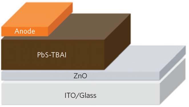

56 TBAI: tetrabutylammonium iodide EDT: 1,2-ethanedithiol PHYS5320 Chapter Nine 56

57 Perovskite solar cells (CH 3 NH 3 PbI 3-x Cl x ) Y. Yang et al., Science 2014, 345, 542. PHYS5320 Chapter Nine 57

58 PHYS5320 Chapter Nine 58


59 W. Y. Nie et al., Science 2015, 347, 522. PHYS5320 Chapter Nine 59

 Q. F. Dong, Y. J. Fang, Y. C. Shao, P. Mulligan, J. Qiu, L. Cao, J. S. Huang, Science 2015, 347, 967.")
60 Perovskite solar cells (CH 3 NH 3 PbI 3-x Cl x ) Large absorption coefficient High carrier mobilities Very small trap density Long carrier lifetime High carrier diffusion length CH 3 NH 3 PbI 3 Electron mobility: 24 cm 2 V 1 s 1 Hole mobility: 164 cm 2 V 1 s 1 Carrier recombination lifetimes: ~100 s (1 sun); ~200 s (0.1 sun) Carrier diffusion lengths: 175 m (1 sun); 3 mm (0.1 sun) Q. F. Dong, Y. J. Fang, Y. C. Shao, P. Mulligan, J. Qiu, L. Cao, J. S. Huang, Science 2015, 347, 967. PHYS5320 Chapter Nine 60
61 Transparent conducting oxides (TCOs) for solar cells TCOs are an increasingly important component of solar cell devices, where they act as electrode elements, structural templates, and diffusion barriers, and their work function controls the open-circuit device voltage. They are employed in applications that range from crystalline-si heterojunctions to organic polymer solar cells. The desirable characteristics of TCO materials include high optical transmissivity across a wide spectrum and low resistivity. Additionally, TCOs for terrestrial solar cell applications must use low-cost materials. Materials that combine optical transparency over much of the solar spectrum with reasonable electrical conductivity generally fall into three classes: very thin pure metals, highly doped conjugated organic polymers, and degenerately doped wide-bandgap oxide or nitride semiconductors. PHYS5320 Chapter Nine 61
62 PHYS5320 Chapter Nine 62

 for a simple cell")
63 This solar cell has achieved record efficiencies (19.2%) for a simple cell geometry. PHYS5320 Chapter Nine 63
 thin-film solar cells have")

64 Copper indium gallium selenide (CIGS) and cadmium telluride (CdTe) thin-film solar cells have demonstrated efficiencies near 20% in the laboratory and have already been in commercial production. PHYS5320 Chapter Nine 64

 Flexed film on a Mylar sheet. (D) AFM image of a 150- nm-thick SWCNT film surface. Z. C.")
65 New Materials: (1) Transparent, Conductive Carbon Nanotube Films (A) Transparent SWCNT films of the indicated thickness on quartz substrates. (B) A large, 80-nm-thick film on a sapphire substrate 10 cm in diameter. (C) Flexed film on a Mylar sheet. (D) AFM image of a 150- nm-thick SWCNT film surface. Z. C. Wu et al. Science 2004, 305, PHYS5320 Chapter Nine 65


66 New Materials: (1) Transparent, Conductive Carbon Nanotube Films PHYS5320 Chapter Nine 66
 SEM image of a MWCNT forest being drawn into a sheet.")
67 New Materials: (1) Transparent, Conductive Carbon Nanotube Films MWCNT forest conversion into sheets. (A) Photograph of a self-supporting 3.4-cm-wide, meter-long MWCNT sheet that has been hand drawn from a nanotube forest at an average rate of 1 m/min. (B) SEM image of a MWCNT forest being drawn into a sheet. (C) SEM micrograph showing the cooperative 90-degree-rotation of MWCNTs in a forest to form a sheet. (D) SEM micrograph of a 2D rereinforced structure fabricated by overlaying four nanotube sheets with a 45-degree-shift in orientation between successive sheets. PHYS5320 Chapter Nine 67
68 New Materials: (1) Transparent, Conductive Carbon Nanotube Films Optical transmittance versus wavelength for a single MWCNT sheet, before and after densification, for light polarized perpendicular to () and parallel to ( ) the draw direction and for unpolarized light (the two curves on the right), where the arrow points from the data for the undensified sample to those for the densified sample. M. Zhang et al. Science 2005, 309, PHYS5320 Chapter Nine 68

 Schematic of a modified electro-spinning setup.")
69 New Materials: (2) Transparent, Conductive Metal Nanowire Films (a) Schematic of the materials method. CuAc 2 /PVA composite fibers were prepared by electro-spinning. The fibers were calcined in air to get CuO nanofibers. The CuO nanofibers were reduced to Cu nanowires by annealing in a H 2 atmosphere. (b) SEM image of Cu nanowires. Scale bar is 10 m. (f) Schematic of a modified electro-spinning setup. (g,h) SEM images of Cu nanowires with controlled orientations. The scale bars are 20 m. PHYS5320 Chapter Nine 69


70 New Materials: (2) Transparent, Conductive Metal Nanowire Films H. Wu et al. Nano Lett. 2010, 10, PHYS5320 Chapter Nine 70
 and dry transfer-printing on a target substrate.")
71 New Materials: (3) Transparent Graphene as Electrodes Schematic of the roll-based production of graphene films grown on a copper foil. The process includes adhesion of polymer supports, copper etching (rinsing) and dry transfer-printing on a target substrate. A wet-chemical doping can be carried out using a setup similar to that used for etching. S. Bae et al. Nat. Nanotechnol. 2010, 5, 574. PHYS5320 Chapter Nine 71

72 New Materials: (3) Transparent Graphene as Electrodes Photographs of the roll-based production of graphene films. (a) Copper foil wrapping around a 7.5-inch quartz tube to be inserted into an 8-inch quartz reactor. The lower image shows the stage in which the copper foil reacts with CH 4 and H 2 gases at high temperatures. (b) Roll-to-roll transfer of graphene films from a thermal release tape to a PET film at 120 C. (c) A transparent ultra-large-area graphene film transferred on a 35-inch PET sheet. (d) Screen printing process of silver paste electrodes on graphene/pet film. The inset shows 3.1-inch graphene/pet panels patterned with silver electrodes before assembly. (e) An assembled graphene/pet touch panel showing outstanding flexibility. (f) A graphene-based touchscreen panel connected to a computer with control software. PHYS5320 Chapter Nine 72

73 New Materials: (3) Transparent Graphene as Electrodes PHYS5320 Chapter Nine 73
74 Reading Materials S. O. Kasap, Optoelectronics and Photonics: Principles and Practices, Prentice Hall, Upper Saddle River, NJ 07458, 2001, Chapter 6, Photovoltaic devices. PHYS5320 Chapter Nine 74
Challenges in to-electric Energy Conversion: an Introduction
 Challenges in Solar-to to-electric Energy Conversion: an Introduction Eray S. Aydil Chemical Engineering and Materials Science Department Acknowledgements: National Science Foundation Minnesota Initiative
PHOTOVOLTAICS Fundamentals
 PHOTOVOLTAICS Fundamentals PV FUNDAMENTALS Semiconductor basics pn junction Solar cell operation Design of silicon solar cell SEMICONDUCTOR BASICS Allowed energy bands Valence and conduction band Fermi
Mesoporous titanium dioxide electrolyte bulk heterojunction
 Mesoporous titanium dioxide electrolyte bulk heterojunction The term "bulk heterojunction" is used to describe a heterojunction composed of two different materials acting as electron- and a hole- transporters,
Chapter 7. Solar Cell
 Chapter 7 Solar Cell 7.0 Introduction Solar cells are useful for both space and terrestrial application. Solar cells furnish the long duration power supply for satellites. It converts sunlight directly
Photovoltaic Energy Conversion. Frank Zimmermann
 Photovoltaic Energy Conversion Frank Zimmermann Solar Electricity Generation Consumes no fuel No pollution No greenhouse gases No moving parts, little or no maintenance Sunlight is plentiful & inexhaustible
Electrons are shared in covalent bonds between atoms of Si. A bound electron has the lowest energy state.
 Photovoltaics Basic Steps the generation of light-generated carriers; the collection of the light-generated carriers to generate a current; the generation of a large voltage across the solar cell; and
Electron Energy, E E = 0. Free electron. 3s Band 2p Band Overlapping energy bands. 3p 3s 2p 2s. 2s Band. Electrons. 1s ATOM SOLID.
 Electron Energy, E Free electron Vacuum level 3p 3s 2p 2s 2s Band 3s Band 2p Band Overlapping energy bands Electrons E = 0 1s ATOM 1s SOLID In a metal the various energy bands overlap to give a single
EE 5611 Introduction to Microelectronic Technologies Fall Tuesday, September 23, 2014 Lecture 07
 EE 5611 Introduction to Microelectronic Technologies Fall 2014 Tuesday, September 23, 2014 Lecture 07 1 Introduction to Solar Cells Topics to be covered: Solar cells and sun light Review on semiconductor
Solar cells operation
 Solar cells operation photovoltaic effect light and dark V characteristics effect of intensity effect of temperature efficiency efficency losses reflection recombination carrier collection and quantum
High efficiency silicon and perovskite-silicon solar cells for electricity generation
 High efficiency silicon and perovskite-silicon solar cells for electricity generation Ali Dabirian Email: dabirian@ipm.ir 1 From Solar Energy to Electricity 2 Global accumulative PV installed In Iran it
Goal for next generation solar cells: Efficiencies greater than Si with low cost (low temperature) processing
 processing") Multi-junction cells MBE growth > 40% efficient Expensive Single crystal Si >20% efficient expensive Thin film cells >10% efficient Less expensive Toxic materials Polymers
Multi-junction cells MBE growth > 40% efficient Expensive Single crystal Si >20% efficient expensive Thin film cells >10% efficient Less expensive Toxic materials Polymers
Photovoltaic cell and module physics and technology
 Photovoltaic cell and module physics and technology Vitezslav Benda, Prof Czech Technical University in Prague benda@fel.cvut.cz www.fel.cvut.cz 6/21/2012 1 Outlines Photovoltaic Effect Photovoltaic cell
OPTI510R: Photonics. Khanh Kieu College of Optical Sciences, University of Arizona Meinel building R.626
 OPTI510R: Photonics Khanh Kieu College of Optical Sciences, University of Arizona kkieu@optics.arizona.edu Meinel building R.626 Announcements Homework #6 is assigned, due May 1 st Final exam May 8, 10:30-12:30pm
Transparent TiO 2 nanotube/nanowire arrays on TCO coated glass substrates: Synthesis and application to solar energy conversion
 Transparent TiO 2 nanotube/nanowire arrays on TCO coated glass substrates: Synthesis and application to solar energy conversion Craig A. Grimes Department of Electrical Engineering Center for Solar Nanomaterials
Supplementary Figure 1 XRD pattern of a defective TiO 2 thin film deposited on an FTO/glass substrate, along with an XRD pattern of bare FTO/glass
 Supplementary Figure 1 XRD pattern of a defective TiO 2 thin film deposited on an FTO/glass substrate, along with an XRD pattern of bare FTO/glass and a reference pattern of anatase TiO 2 (JSPDS No.: 21-1272).
Photovoltaic cell and module physics and technology. Vitezslav Benda, Prof Czech Technical University in Prague
 Photovoltaic cell and module physics and technology Vitezslav Benda, Prof Czech Technical University in Prague benda@fel.cvut.cz www.fel.cvut.cz 1 Outlines Photovoltaic Effect Photovoltaic cell structure
Towards a deeper understanding of polymer solar cells
 Towards a deeper understanding of polymer solar cells Jan Anton Koster Valentin Mihailetchi Prof. Paul Blom Molecular Electronics Zernike Institute for Advanced Materials and DPI University of Groningen
Title of file for HTML: Supplementary Information Description: Supplementary Figures and Supplementary References
 Title of file for HTML: Supplementary Information Description: Supplementary Figures and Supplementary References Supplementary Figure 1. SEM images of perovskite single-crystal patterned thin film with
Classification of Solids
 Classification of Solids Classification by conductivity, which is related to the band structure: (Filled bands are shown dark; D(E) = Density of states) Class Electron Density Density of States D(E) Examples
LEC E T C U T R U E R E 17 -Photodetectors
 LECTURE 17 -Photodetectors Topics to be covered Photodetectors PIN photodiode Avalanche Photodiode Photodetectors Principle of the p-n junction Photodiode A generic photodiode. Photodetectors Principle
Chemistry Instrumental Analysis Lecture 8. Chem 4631
 Chemistry 4631 Instrumental Analysis Lecture 8 UV to IR Components of Optical Basic components of spectroscopic instruments: stable source of radiant energy transparent container to hold sample device
Lecture 12. Semiconductor Detectors - Photodetectors
 Lecture 12 Semiconductor Detectors - Photodetectors Principle of the pn junction photodiode Absorption coefficient and photodiode materials Properties of semiconductor detectors The pin photodiodes Avalanche
1 Name: Student number: DEPARTMENT OF PHYSICS AND PHYSICAL OCEANOGRAPHY MEMORIAL UNIVERSITY OF NEWFOUNDLAND. Fall :00-11:00
 1 Name: DEPARTMENT OF PHYSICS AND PHYSICAL OCEANOGRAPHY MEMORIAL UNIVERSITY OF NEWFOUNDLAND Final Exam Physics 3000 December 11, 2012 Fall 2012 9:00-11:00 INSTRUCTIONS: 1. Answer all seven (7) questions.
Supplementary Figure 1. Supplementary Figure 1 Characterization of another locally gated PN junction based on boron
 Supplementary Figure 1 Supplementary Figure 1 Characterization of another locally gated PN junction based on boron nitride and few-layer black phosphorus (device S1). (a) Optical micrograph of device S1.
ET3034TUx Utilization of band gap energy
 ET3034TUx - 3.3.1 - Utilization of band gap energy In the last two weeks we have discussed the working principle of a solar cell and the external parameters that define the performance of a solar cell.
Fundamentals of Photovoltaics: C1 Problems. R.Treharne, K. Durose, J. Major, T. Veal, V.
 Fundamentals of Photovoltaics: C1 Problems R.Treharne, K. Durose, J. Major, T. Veal, V. Dhanak @cdtpv November 3, 2015 These problems will be highly relevant to the exam that you will sit very shortly.
Chapter 4. Photodetectors
 Chapter 4 Photodetectors Types of photodetectors: Photoconductos Photovoltaic Photodiodes Avalanche photodiodes (APDs) Resonant-cavity photodiodes MSM detectors In telecom we mainly use PINs and APDs.
Solar Cells Based on. Quantum Dots: Multiple Exciton Generation and Intermediate Bands Antonio Luque, Antonio Marti, and Arthur J.
 Solar Cells Based on Quantum Dots: Multiple Exciton Generation and Intermediate Bands Antonio Luque, Antonio Marti, and Arthur J. Nozik Student ID: 2004171039 Name: Yo-Han Choi Abstract Semiconductor quantum
Photovoltaics. Lecture 7 Organic Thin Film Solar Cells Photonics - Spring 2017 dr inż. Aleksander Urbaniak
 Photovoltaics Lecture 7 Organic Thin Film Solar Cells Photonics - Spring 2017 dr inż. Aleksander Urbaniak Barcelona, Spain Perpignan train station, France source: pinterest Why organic solar cells? 1.
PRESENTED BY: PROF. S. Y. MENSAH F.A.A.S; F.G.A.A.S UNIVERSITY OF CAPE COAST, GHANA.
 SOLAR CELL AND ITS APPLICATION PRESENTED BY: PROF. S. Y. MENSAH F.A.A.S; F.G.A.A.S UNIVERSITY OF CAPE COAST, GHANA. OUTLINE OF THE PRESENTATION Objective of the work. A brief introduction to Solar Cell
(Co-PIs-Mark Brongersma, Yi Cui, Shanhui Fan) Stanford University. GCEP Research Symposium 2013 Stanford, CA October 9, 2013
 Stanford University. GCEP Research Symposium 2013 Stanford, CA October 9, 2013") High-efficiency thin film nano-structured multi-junction solar James S. cells Harris (PI) (Co-PIs-Mark Brongersma, Yi Cui, Shanhui Fan) Stanford University GCEP Research Symposium 2013 Stanford, CA October
High-efficiency thin film nano-structured multi-junction solar James S. cells Harris (PI) (Co-PIs-Mark Brongersma, Yi Cui, Shanhui Fan) Stanford University GCEP Research Symposium 2013 Stanford, CA October
Basic Limitations to Third generation PV performance
 Basic Limitations to Third generation PV performance Pabitra K. Nayak Weizmann Institute of Science, Rehovot, Israel THANKS to my COLLEAGUES Lee Barnea and David Cahen. Weizmann Institute of Science Juan
Photoconductive Atomic Force Microscopy for Understanding Nanostructures and Device Physics of Organic Solar Cells
 Photoconductive AFM of Organic Solar Cells APP NOTE 15 Photoconductive Atomic Force Microscopy for Understanding Nanostructures and Device Physics of Organic Solar Cells Xuan-Dung Dang and Thuc-Quyen Nguyen
3.1 Introduction to Semiconductors. Y. Baghzouz ECE Department UNLV
 3.1 Introduction to Semiconductors Y. Baghzouz ECE Department UNLV Introduction In this lecture, we will cover the basic aspects of semiconductor materials, and the physical mechanisms which are at the
The Current Status of Perovskite Solar Cell Research at UCLA
 The Current Status of Perovskite Solar Cell Research at UCLA Lijian Zuo, Sanghoon Bae, Lei Meng, Yaowen Li, and Yang Yang* Department of Materials Science and Engineering University of California, Los
February 1, 2011 The University of Toledo, Department of Physics and Astronomy SSARE, PVIC
 FUNDAMENTAL PROPERTIES OF SOLAR CELLS February 1, 2011 The University of Toledo, Department of Physics and Astronomy SSARE, PVIC Principles and Varieties of Solar Energy (PHYS 4400) and Fundamentals of
Chapter 6: Light-Emitting Diodes
 Chapter 6: Light-Emitting Diodes Photoluminescence and electroluminescence Basic transitions Luminescence efficiency Light-emitting diodes Internal quantum efficiency External quantum efficiency Device
A. K. Das Department of Physics, P. K. College, Contai; Contai , India.
 IOSR Journal of Applied Physics (IOSR-JAP) e-issn: 2278-4861.Volume 7, Issue 2 Ver. II (Mar. - Apr. 2015), PP 08-15 www.iosrjournals.org Efficiency Improvement of p-i-n Structure over p-n Structure and
Analyze the effect of window layer (AlAs) for increasing the efficiency of GaAs based solar cell
 for increasing the efficiency of GaAs based solar cell") American Journal of Engineering Research (AJER) e-issn: 2320-0847 p-issn : 2320-0936 Volume-4, Issue-7, pp-304-315 www.ajer.org Research Paper Open Access Analyze the effect of window layer (AlAs) for
American Journal of Engineering Research (AJER) e-issn: 2320-0847 p-issn : 2320-0936 Volume-4, Issue-7, pp-304-315 www.ajer.org Research Paper Open Access Analyze the effect of window layer (AlAs) for
Nanostructured Semiconductor Crystals -- Building Blocks for Solar Cells: Shapes, Syntheses, Surface Chemistry, Quantum Confinement Effects
 Nanostructured Semiconductor Crystals -- Building Blocks for Solar Cells: Shapes, Syntheses, Surface Chemistry, Quantum Confinement Effects April 1,2014 The University of Toledo, Department of Physics
MODELING THE FUNDAMENTAL LIMIT ON CONVERSION EFFICIENCY OF QD SOLAR CELLS
 MODELING THE FUNDAMENTAL LIMIT ON CONVERSION EFFICIENCY OF QD SOLAR CELLS Ա.Մ.Կեչիյանց Ara Kechiantz Institute of Radiophysics and Electronics (IRPhE), National Academy of Sciences (Yerevan, Armenia) Marseille
Introduction. Katarzyna Skorupska. Silicon will be used as the model material however presented knowledge applies to other semiconducting materials
 Introduction Katarzyna Skorupska Silicon will be used as the model material however presented knowledge applies to other semiconducting materials 2 June 26 Intrinsic and Doped Semiconductors 3 July 3 Optical
Stanford University MatSci 152: Principles of Electronic Materials and Devices Spring Quarter, Final Exam, June 8, 2010
 Stanford University MatSci 152: Principles of Electronic Materials and Devices Spring Quarter, 2009-2010 Final Exam, June 8, 2010 This is a closed book, closed notes exam. You are allowed two double-sided
Charge Extraction from Complex Morphologies in Bulk Heterojunctions. Michael L. Chabinyc Materials Department University of California, Santa Barbara
 Charge Extraction from Complex Morphologies in Bulk Heterojunctions Michael L. Chabinyc Materials Department University of California, Santa Barbara OPVs Vs. Inorganic Thin Film Solar Cells Alta Devices
Solar Cell Materials and Device Characterization
 Solar Cell Materials and Device Characterization April 3, 2012 The University of Toledo, Department of Physics and Astronomy SSARE, PVIC Principles and Varieties of Solar Energy (PHYS 4400) and Fundamentals
Organic Solar Cells. All Organic solar cell. Dye-sensitized solar cell. Dye. τ inj. τ c. τ r surface states D*/D + V o I 3 D/D.
 The 4th U.S.-Korea NanoForum April 26-27, 2007, Honolulu, USA Improvement of Device Efficiency in Conjugated Polymer/Fullerene NanoComposite Solar Cells School of Semiconductor & Chemical Engineering *
NANO TECHNOLOGY IN POLYMER SOLAR CELLS. Mayur Padharia, Hardik Panchal, Keval Shah, *Neha Patni, Shibu.G.Pillai
 NANO TECHNOLOGY IN POLYMER SOLAR CELLS Mayur Padharia, Hardik Panchal, Keval Shah, *Neha Patni, Shibu.G.Pillai Department of Chemical Engineering, Institute of Technology, Nirma University, S. G. Highway,
The Opto-Electronic Physics That Just Broke the Efficiency Record in Solar Cells
 The Opto-Electronic Physics That Just Broke the Efficiency Record in Solar Cells Solar Energy Mini-Series Jen-Hsun Huang Engineering Center Stanford, California Sept. 26, 2011 Owen D. Miller & Eli Yablonovitch
FYS 3028/8028 Solar Energy and Energy Storage. Calculator with empty memory Language dictionaries
 Faculty of Science and Technology Exam in: FYS 3028/8028 Solar Energy and Energy Storage Date: 11.05.2016 Time: 9-13 Place: Åsgårdvegen 9 Approved aids: Type of sheets (sqares/lines): Number of pages incl.
Planar Organic Photovoltaic Device. Saiful I. Khondaker
 Planar Organic Photovoltaic Device Saiful I. Khondaker Nanoscience Technology Center and Department of Physics University of Central Florida http://www.physics.ucf.edu/~khondaker W Metal 1 L ch Metal 2
Chapter 1 Overview of Semiconductor Materials and Physics
 Chapter 1 Overview of Semiconductor Materials and Physics Professor Paul K. Chu Conductivity / Resistivity of Insulators, Semiconductors, and Conductors Semiconductor Elements Period II III IV V VI 2 B
Quantum Dots for Advanced Research and Devices
 Quantum Dots for Advanced Research and Devices spectral region from 450 to 630 nm Zero-D Perovskite Emit light at 520 nm ABOUT QUANTUM SOLUTIONS QUANTUM SOLUTIONS company is an expert in the synthesis
Supplementary Figure 1 Scheme image of GIXD set-up. The scheme image of slot die
 Supplementary Figure 1 Scheme image of GIXD set-up. The scheme image of slot die printing system combined with grazing incidence X-ray diffraction (GIXD) set-up. 1 Supplementary Figure 2 2D GIXD images
Lecture 15: Optoelectronic devices: Introduction
 Lecture 15: Optoelectronic devices: Introduction Contents 1 Optical absorption 1 1.1 Absorption coefficient....................... 2 2 Optical recombination 5 3 Recombination and carrier lifetime 6 3.1
e - Galvanic Cell 1. Voltage Sources 1.1 Polymer Electrolyte Membrane (PEM) Fuel Cell
 Fuel Cell") Galvanic cells convert different forms of energy (chemical fuel, sunlight, mechanical pressure, etc.) into electrical energy and heat. In this lecture, we are interested in some examples of galvanic cells.
Galvanic cells convert different forms of energy (chemical fuel, sunlight, mechanical pressure, etc.) into electrical energy and heat. In this lecture, we are interested in some examples of galvanic cells.
Supplemental Discussion for Multijunction Solar Cell Efficiencies: Effect of Spectral Window, Optical Environment and Radiative Coupling
 Electronic Supplementary Material (ESI) for Energy & Environmental Science. This journal is The Royal Society of Chemistry 2014 Supplemental Discussion for Multijunction Solar Cell Efficiencies: Effect
Introduction to Organic Solar Cells
 Introduction to Organic Solar Cells Dr Chris Fell Solar Group Leader CSIRO Energy Technology, Newcastle, Australia Organic semiconductors Conductivity in polyacetylene 1970s Nobel Prize Alan J. Heeger
Flexible Organic Photovoltaics Employ laser produced metal nanoparticles into the absorption layer 1. An Introduction
 Flexible Organic Photovoltaics Employ laser produced metal nanoparticles into the absorption layer 1. An Introduction Among the renewable energy sources that are called to satisfy the continuously increased
Development of active inks for organic photovoltaics: state-of-the-art and perspectives
 Development of active inks for organic photovoltaics: state-of-the-art and perspectives Jörg Ackermann Centre Interdisciplinaire de Nanoscience de Marseille (CINAM) CNRS - UPR 3118, MARSEILLE - France
Modeling of the Current-Voltage Characteristics of CdTe Thin-Film and Bulk Heterojunction Organic Solar Cells
 Modeling of the Current-Voltage Characteristics of CdTe Thin-Film and Bulk Heterojunction Organic Solar Cells Salman Moazzem Arnab A Thesis in the Department of Electrical and Computer Engineering Presented
Atmospheric pressure Plasma Enhanced CVD for large area deposition of TiO 2-x electron transport layers for PV. Heather M. Yates
 Atmospheric pressure Plasma Enhanced CVD for large area deposition of TiO 2-x electron transport layers for PV Heather M. Yates Why the interest? Perovskite solar cells have shown considerable promise
Comparison of Ge, InGaAs p-n junction solar cell
 ournal of Physics: Conference Series PAPER OPEN ACCESS Comparison of Ge, InGaAs p-n junction solar cell To cite this article: M. Korun and T. S. Navruz 16. Phys.: Conf. Ser. 77 135 View the article online
Lecture 5 Junction characterisation
 Lecture 5 Junction characterisation Jon Major October 2018 The PV research cycle Make cells Measure cells Despair Repeat 40 1.1% 4.9% Data Current density (ma/cm 2 ) 20 0-20 -1.0-0.5 0.0 0.5 1.0 Voltage
Chapter 5. Semiconductor Laser
 Chapter 5 Semiconductor Laser 5.0 Introduction Laser is an acronym for light amplification by stimulated emission of radiation. Albert Einstein in 1917 showed that the process of stimulated emission must
ELECTRONIC DEVICES AND CIRCUITS SUMMARY
 ELECTRONIC DEVICES AND CIRCUITS SUMMARY Classification of Materials: Insulator: An insulator is a material that offers a very low level (or negligible) of conductivity when voltage is applied. Eg: Paper,
Organic solar cells. State of the art and outlooks. Gilles Horowitz LPICM, UMR7647 CNRS - Ecole Polytechnique
 Organic solar cells. State of the art and outlooks Gilles Horowitz LPICM, UMR7647 CNRS - Ecole Polytechnique Solar energy Solar energy on earth: 75,000 tep/year 6000 times the world consumption in 2007
Third generation solar cells - How to use all the pretty colours?
 Third generation solar cells - How to use all the pretty colours? Erik Stensrud Marstein Department for Solar Energy Overview The trouble with conventional solar cells Third generation solar cell concepts
Opto-electronic Characterization of Perovskite Thin Films & Solar Cells
 Opto-electronic Characterization of Perovskite Thin Films & Solar Cells Arman Mahboubi Soufiani Supervisors: Prof. Martin Green Prof. Gavin Conibeer Dr. Anita Ho-Baillie Dr. Murad Tayebjee 22 nd June 2017
Boosting the Performance of Solar Cells with Intermediate Band Absorbers The Case of ZnTe:O
 Journal of Energy and Power Engineering 11 (2017) 417-426 doi: 10.17265/1934-8975/2017.06.007 D DAVID PUBLISHING Boosting the Performance of Solar Cells with Intermediate Band Absorbers The Case of ZnTe:O
Conjugated Polymers Based on Benzodithiophene for Organic Solar Cells. Wei You
 Wake Forest Nanotechnology Conference October 19, 2009 Conjugated Polymers Based on Benzodithiophene for Organic olar Cells Wei You Department of Chemistry and Institute for Advanced Materials, Nanoscience
Quantum Dot Technology for Low-Cost Space Power Generation for Smallsats
 SSC06-VI- Quantum Dot Technology for Low-Cost Space Power Generation for Smallsats Theodore G. DR Technologies, Inc. 7740 Kenamar Court, San Diego, CA 92020 (858)677-230 tstern@drtechnologies.com The provision
SEMICONDUCTOR PHYSICS REVIEW BONDS,
 SEMICONDUCTOR PHYSICS REVIEW BONDS, BANDS, EFFECTIVE MASS, DRIFT, DIFFUSION, GENERATION, RECOMBINATION February 3, 2011 The University of Toledo, Department of Physics and Astronomy SSARE, PVIC Principles
1. Depleted heterojunction solar cells. 2. Deposition of semiconductor layers with solution process. June 7, Yonghui Lee
 1. Depleted heterojunction solar cells 2. Deposition of semiconductor layers with solution process June 7, 2016 Yonghui Lee Outline 1. Solar cells - P-N junction solar cell - Schottky barrier solar cell
Nanotechnology and Solar Energy. Solar Electricity Photovoltaics. Fuel from the Sun Photosynthesis Biofuels Split Water Fuel Cells
 Nanotechnology and Solar Energy Solar Electricity Photovoltaics Fuel from the Sun Photosynthesis Biofuels Split Water Fuel Cells Solar cell A photon from the Sun generates an electron-hole pair in a semiconductor.
Laser Basics. What happens when light (or photon) interact with a matter? Assume photon energy is compatible with energy transition levels.
 interact with a matter? Assume photon energy is compatible with energy transition levels.") What happens when light (or photon) interact with a matter? Assume photon energy is compatible with energy transition levels. Electron energy levels in an hydrogen atom n=5 n=4 - + n=3 n=2 13.6 = [ev]
What happens when light (or photon) interact with a matter? Assume photon energy is compatible with energy transition levels. Electron energy levels in an hydrogen atom n=5 n=4 - + n=3 n=2 13.6 = [ev]
Theoretical Study on Graphene Silicon Heterojunction Solar Cell
 Copyright 2015 American Scientific Publishers All rights reserved Printed in the United States of America Journal of Nanoelectronics and Optoelectronics Vol. 10, 1 5, 2015 Theoretical Study on Graphene
Fundamental Limitations of Solar Cells
 2018 Lecture 2 Fundamental Limitations of Solar Cells Dr Kieran Cheetham MPhys (hons) CPhys MInstP MIET L3 Key Question Why can't a solar cell have a 100% efficiency? (Or even close to 100%?) Can you answer
Thermionic Current Modeling and Equivalent Circuit of a III-V MQW P-I-N Photovoltaic Heterostructure
 Thermionic Current Modeling and Equivalent Circuit of a III-V MQW P-I-N Photovoltaic Heterostructure ARGYRIOS C. VARONIDES Physics and Electrical Engineering Department University of Scranton 800 Linden
Novel Inorganic-Organic Perovskites for Solution Processed Photovoltaics. PIs: Mike McGehee and Hema Karunadasa
 Novel Inorganic-Organic Perovskites for Solution Processed Photovoltaics PIs: Mike McGehee and Hema Karunadasa 1 Perovskite Solar Cells are Soaring Jul 2013 Grätzel, EPFL 15% Nov 2014 KRICT 20.1%! Seok,
Stimulated Emission Devices: LASERS
 Stimulated Emission Devices: LASERS 1. Stimulated Emission and Photon Amplification E 2 E 2 E 2 hυ hυ hυ In hυ Out hυ E 1 E 1 E 1 (a) Absorption (b) Spontaneous emission (c) Stimulated emission The Principle
EE 5344 Introduction to MEMS CHAPTER 5 Radiation Sensors
 EE 5344 Introduction to MEMS CHAPTER 5 Radiation Sensors 5. Radiation Microsensors Radiation µ-sensors convert incident radiant signals into standard electrical out put signals. Radiant Signals Classification
Photonic Devices Human eye: about 400 nm to 700 nm
 Photonic Devices Human eye: about 400 nm to 700 nm λ [ nm] = 1240 E[ ev ] S. M. Sze, Physics of Semiconductor Devices Sensitivity of the human eye Two LEDs: red (λ = 660 nm) green (λ = 560 nm) emitting
NSF EPSCoR Kansas Center for Solar Energy Research Annual Program Review June 12-14, 2011
 NSF EPSCoR Kansas Center for Solar Energy Research Annual Program Review June 12-14, 2011 Plasmonic and Photonic Photovoltaics based on graphene and other carbon nanostructures Fengli Wang, Guowei Xu,
EE 6313 Homework Assignments
 EE 6313 Homework Assignments 1. Homework I: Chapter 1: 1.2, 1.5, 1.7, 1.10, 1.12 [Lattice constant only] (Due Sept. 1, 2009). 2. Homework II: Chapter 1, 2: 1.17, 2.1 (a, c) (k = π/a at zone edge), 2.3
Supplementary material for High responsivity mid-infrared graphene detectors with antenna-enhanced photo-carrier generation and collection
 Supplementary material for High responsivity mid-infrared graphene detectors with antenna-enhanced photo-carrier generation and collection Yu Yao 1, Raji Shankar 1, Patrick Rauter 1, Yi Song 2, Jing Kong
EE 446/646 Photovoltaic Devices I. Y. Baghzouz
 EE 446/646 Photovoltaic Devices I Y. Baghzouz What is Photovoltaics? First used in about 1890, the word has two parts: photo, derived from the Greek word for light, volt, relating to electricity pioneer
Research Article P3HT:PCBM Incorporated with Silicon Nanoparticles as Photoactive Layer in Efficient Organic Photovoltaic Devices
 Nanomaterials Volume 2013, Article ID 354035, 4 pages http://dx.doi.org/10.1155/2013/354035 Research Article P3HT:PCBM Incorporated with Silicon Nanoparticles as Photoactive Layer in Efficient Organic
OPTI510R: Photonics. Khanh Kieu College of Optical Sciences, University of Arizona Meinel building R.626
 OPTI510R: Photonics Khanh Kieu College of Optical Sciences, University of Arizona kkieu@optics.arizona.edu Meinel building R.626 Announcements HW#3 is assigned due Feb. 20 st Mid-term exam Feb 27, 2PM
status solidi R. Ulbricht, X. Jiang, S. Lee, K. Inoue, M. Zhang, S. Fang, R. Baughman, and A. Zakhidov
 physica pss www.pss-b.com status solidi basic solid state physics b Polymeric solar cells with oriented and strong transparent carbon nanotube anode R. Ulbricht, X. Jiang, S. Lee, K. Inoue, M. Zhang, S.
Vikram Kuppa School of Energy, Environmental, Biological and Medical Engineering College of Engineering and Applied Science University of Cincinnati
 Vikram Kuppa School of Energy, Environmental, Biological and Medical Engineering College of Engineering and Applied Science University of Cincinnati vikram.kuppa@uc.edu Fei Yu Yan Jin Andrew Mulderig Greg
Chapter 1. Solar energy conversion: from amorphous silicon to Dye-Sensitized Solar Cells. 1.1 Photovoltaic history.
 Chapter 1 Solar energy conversion: from amorphous silicon to Dye-Sensitized Solar Cells 1.1 Photovoltaic history. 1.2 Operation of traditional photovoltaic devices. 1.3 Thin film solar cells. 1.4 Multijunction
Photovoltaic Enhancement Due to Surface-Plasmon Assisted Visible-Light. Absorption at the Inartificial Surface of Lead Zirconate-Titanate Film
 Photovoltaic Enhancement Due to Surface-Plasmon Assisted Visible-Light Absorption at the Inartificial Surface of Lead Zirconate-Titanate Film Fengang Zheng, a,b, * Peng Zhang, a Xiaofeng Wang, a Wen Huang,
The Role of doping in the window layer on Performance of a InP Solar Cells USING AMPS-1D
 IOSR Journal of Engineering (IOSRJEN) ISSN: 2250-3021 Volume 2, Issue 8(August 2012), PP 42-46 The Role of doping in the window layer on Performance of a InP Solar Cells USING AMPS-1D Dennai Benmoussa
More Efficient Solar Cells via Multi Exciton Generation
 More Efficient Solar Cells via Multi Exciton Generation By: MIT Student Instructor: Gang Chen May 14, 2010 1 Introduction Sunlight is the most abundant source of energy available on Earth and if properly
What will it take for organic solar cells to be competitive?
 What will it take for organic solar cells to be competitive? Michael D. McGehee Stanford University Director of the Center for Advanced Molecular Photovoltaics Efficiency (%) We will need 20-25 % efficiency
Engineering 2000 Chapter 8 Semiconductors. ENG2000: R.I. Hornsey Semi: 1
 Engineering 2000 Chapter 8 Semiconductors ENG2000: R.I. Hornsey Semi: 1 Overview We need to know the electrical properties of Si To do this, we must also draw on some of the physical properties and we
Quantum Dot Solar Cells
 Quantum Dot Solar Cells 2 INTRODUCTION: As industrialization speeds up in developing and under-developed countries with an alarming rise in population, global power consumption has become a big question
Solar Cells Technology: An Engine for National Development
 IOSR Journal of Electrical and Electronics Engineering (IOSR-JEEE) e-issn: 2278-1676,p-ISSN: 2320-3331, Volume 7, Issue 5 (Sep. - Oct. 2013), PP 13-18 Solar Cells Technology: An Engine for National Development
Organic Electronic Devices
 Organic Electronic Devices Week 4: Organic Photovoltaic Devices Lecture 4.2: Characterizing Device Parameters in OPVs Bryan W. Boudouris Chemical Engineering Purdue University 1 Lecture Overview and Learning
Multiple Exciton Generation in Quantum Dots. James Rogers Materials 265 Professor Ram Seshadri
 Multiple Exciton Generation in Quantum Dots James Rogers Materials 265 Professor Ram Seshadri Exciton Generation Single Exciton Generation in Bulk Semiconductors Multiple Exciton Generation in Bulk Semiconductors