Unit 02 Modules Systems. Components. Marcus Rennhofer : Modules, Systems & Components
|
|
|
- Kristina Curtis
- 5 years ago
- Views:
Transcription


1 Unit 02 Modules Systems Marcus Rennhofer
2 Content: Systems & System System types Module & Inverter Solar batteries Electric circuit Technology Families Crystalline solar cells Thin film solar cells next generation Resources Abundancy of resources

3 1. SYSTEM TYPES
 Free-field Roof-Top")
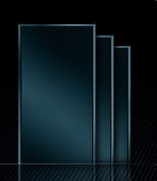
4 1. System types: Grid connected Type of installation: (Austria) Free-field Roof-Top Buildingintegrated


5 1. System types: Grid connected Typical applications: residential houses industrial roof tops free field installations Augsburger Passive house center ATB-Becker

 (ETECH,")
6 1. System types: Grid connected Feed in the grid Sur-plus feed in (ETECH, 2012) (ETECH, 2012)


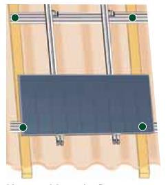
7 1. System types: roof top mounted - Roof hooks - Clamps - Mounted onto common rafter (Schletter, 2013)


8 1. System types: mounting types - Point mounted - Line mounted - Fast mounting (Schletter, 2013)


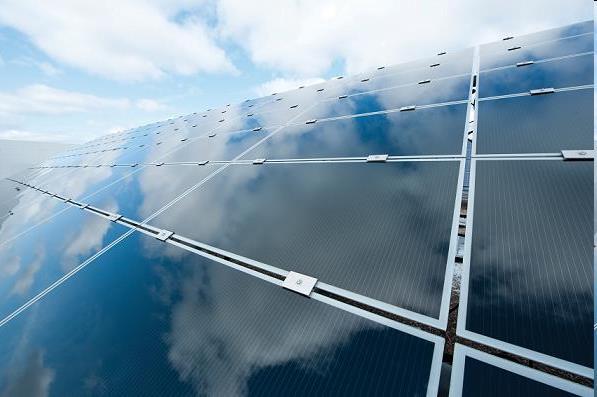
9 1. System types: grid connected: free field - Fixed mounting - 2-Axial Tracker


10 1. System types: grid connected: free field - Fixed mounting 13 MW 7 MW (AIT, 2014)

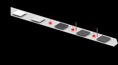
11 1. System types: grid connected: free field: X-Module mounted (Enerparc 2017)

12 1. System types: grid connected: free field: PV for horizontal agricultural areas Can be installed on the farmland water and irradiance control Double use of area

13 1. System types: grid connected: free field: PV for horizontal agricultural areas PV as wind shield small foot print PV-Magazin.de, next2sun


 Central-Inv.")
 (Power One,")
14 1. System types: Grid connected: Inverter Module-Inv. (300W) String-Inv. (kw) Central-Inv. (MW) (Power One, 2014) (Power One, 2014) (Power One, 2014)

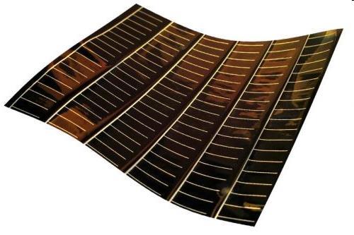
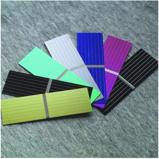
15 1. System types: Grid connected


16 1. System DC switch Grid connected Connection box / over voltage protection

 Decentralized infrastructure (")

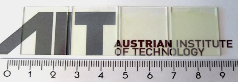
17 1. System types: Island system Typical applications: Free standing houses (mountain huts) Rural areas (not grid connected) Decentralized infrastructure ( weather stations, traffic signals, ) House boat with PV Mongolian Neue Donau, yurt with Vienna PV ATB-Becker

18 1. System types: Island system

19 1. System Island system


20 1. System Types: Hybrid Decentralized components & Grid connection Several power units Schiestlhaus Hochschwab ATB-Becker

21 2. TECHNOLOGY FAMILIES
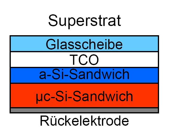
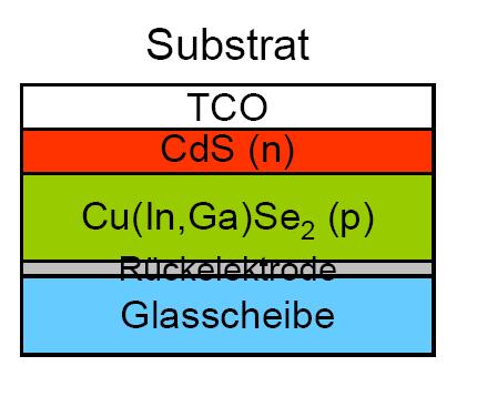
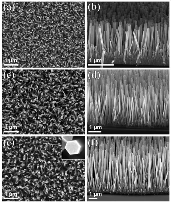
22 2. Technology Types: Family - Tree Cell types Metal-Oxide Perovskite Crystalline Hybrid Thin Film Poly crystalline (pc) Mono crystalline / Wafer M. c. / back contacted M. c. / spherical grains HIT (mono + a-si) µsi/a-si (Multi-Junction) Mono Si Thin Film Inorganic / organic Mono / GaAs Tandem: two oth. types Amorphous Silicide, a-si CuInSe / Cu(In,Ga)Se 2 CdTe GaAs / InGaAs organic Dye sensitized CZTS

 Up to Semi-")

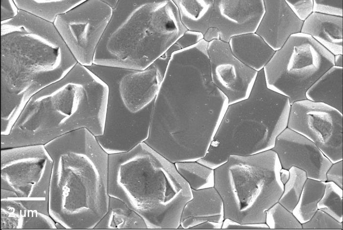
23 2. Technology Types: Cyristalline ~ 250 m Si cell Czochralski: Purity > % (6N) Up to Semi- Conductor-Si > 9N Si single crystal Poly crystaline cell ( multi cyristaline ) Single crystal corns domains

24 2. Production: Solar cell grow: Czochralski (epull from crucible)

25 2. production : crystaline Si Module


26 2. Technology Types: Crystalline h > 20% Modules up to: 345 W
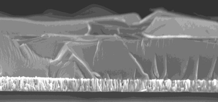
27 2. Production: Thin film photovoltaics (TF)
")

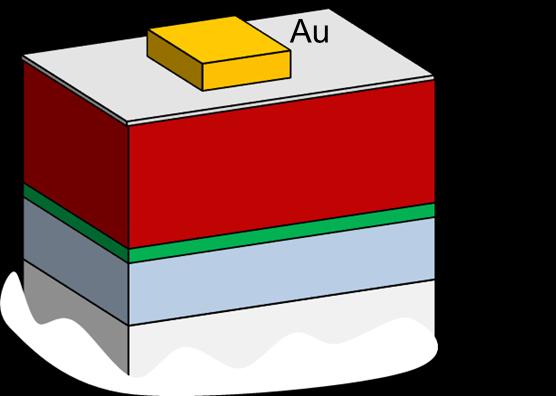
28 2. Processes: TF-PV via chemical bath deposition (CBD) non-vacuum, low-cost, up-scalable, R2R compatible, min. material consumption
29 2. Technology Types: a-si, CdTe, CIGS

30 2. Technology Types: a-si, CdTe, CIGS
 / Grätzel Technical problems:")

31 2. Technology Types: next gen. : dye-sensitized (DSSC) / Grätzel Technical problems: e-transport Ion - mobility ohmic losses fluid dynamics corrosive Advantages: cheap low-tech abundant ressources flexible substrate transparent H.glass

")
32 2. Technology Types: next gen. : Organic Polymer- fullerene- Nanoparticle - mixture: low efficiency fast ageing (< 5a) Merck
 4 Low efficencies")
33 2. Technology Types: next gen. : CZTS Cu 2 ZnSn(S,Se) 4 Low efficencies Abundant elements IBM


34 2. Technology Types: next gen. : Mono crystalline CZTS crystalsol

35 2. Technology Types: next gen. : Metal oxides (CuO 2 ) 1 µm (c) (d) Abundant Vivid colors


36 2. Technology Types: next gen. : Perovskites


37 2. Technology Types: next gen. : Mono crystalline Si sphere


38 2. Technology Types: next gen. : GaAs / GaInAs h > 30% ESA-goal 2017: 34-37% Helmholzzentrum Berlin EUR /m 2
39 2. Technology Types: next gen. : X on Y Old: New: c-si / a-si c-si / Pero c-si / OPV CIGS / Pero Pero / OPV High voltages High currents Band gap matching


40 3. Resources & Abundancy
41 3. Abundancy Faulstich, TU-München
42 3. Abundancy Faulstich, TU-München

43 3. Abundancy Faulstich, TU-München

44 3. Abundancy Faulstich, TU-München
 2002: 97 $/kg 2012: 900 $/kg 2016: 1200 $ /kg Te production: 400 t/a (2016)")
45 3. Abundancy In-Prize: (99.99%) 2002: 97 $/kg 2012: 900 $/kg 2016: 1200 $ /kg Te production: 400 t/a (2016) Side product of Cu, Ni- Industry SiO 2 27% earth crust = Si

46 Thank you for your attention! AIT (CuO 2 / ZnO-nw)
Goal for next generation solar cells: Efficiencies greater than Si with low cost (low temperature) processing
 processing") Multi-junction cells MBE growth > 40% efficient Expensive Single crystal Si >20% efficient expensive Thin film cells >10% efficient Less expensive Toxic materials Polymers
Multi-junction cells MBE growth > 40% efficient Expensive Single crystal Si >20% efficient expensive Thin film cells >10% efficient Less expensive Toxic materials Polymers
Mesoporous titanium dioxide electrolyte bulk heterojunction
 Mesoporous titanium dioxide electrolyte bulk heterojunction The term "bulk heterojunction" is used to describe a heterojunction composed of two different materials acting as electron- and a hole- transporters,
High efficiency silicon and perovskite-silicon solar cells for electricity generation
 High efficiency silicon and perovskite-silicon solar cells for electricity generation Ali Dabirian Email: dabirian@ipm.ir 1 From Solar Energy to Electricity 2 Global accumulative PV installed In Iran it
Photovoltaic cell and module physics and technology
 Photovoltaic cell and module physics and technology Vitezslav Benda, Prof Czech Technical University in Prague benda@fel.cvut.cz www.fel.cvut.cz 6/21/2012 1 Outlines Photovoltaic Effect Photovoltaic cell
Energy Yield. Marcus Rennhofer Unit : Energy Yield
 Energy Yield Marcus Rennhofer marcus.rennhofer@ait.ac.at Unit 11 Content Energy Yield Annual energy yield Generator quality measures Losses of energy Modelling Types of models Concepts of models Analytic
Development of active inks for organic photovoltaics: state-of-the-art and perspectives
 Development of active inks for organic photovoltaics: state-of-the-art and perspectives Jörg Ackermann Centre Interdisciplinaire de Nanoscience de Marseille (CINAM) CNRS - UPR 3118, MARSEILLE - France
Challenges in to-electric Energy Conversion: an Introduction
 Challenges in Solar-to to-electric Energy Conversion: an Introduction Eray S. Aydil Chemical Engineering and Materials Science Department Acknowledgements: National Science Foundation Minnesota Initiative
Photovoltaic cell and module physics and technology. Vitezslav Benda, Prof Czech Technical University in Prague
 Photovoltaic cell and module physics and technology Vitezslav Benda, Prof Czech Technical University in Prague benda@fel.cvut.cz www.fel.cvut.cz 1 Outlines Photovoltaic Effect Photovoltaic cell structure
Chapter 1. Solar energy conversion: from amorphous silicon to Dye-Sensitized Solar Cells. 1.1 Photovoltaic history.
 Chapter 1 Solar energy conversion: from amorphous silicon to Dye-Sensitized Solar Cells 1.1 Photovoltaic history. 1.2 Operation of traditional photovoltaic devices. 1.3 Thin film solar cells. 1.4 Multijunction
Solliance. Perovskite based PV (PSC) Program. TKI Urban Energy Days l e d b y i m e c, E C N a n d T N O
 Program. TKI Urban Energy Days l e d b y i m e c, E C N a n d T N O") Solliance Perovskite based PV (PSC) Program TKI Urban Energy Days - 2017-06-21 l e d b y i m e c, E C N a n d T N O 2 Bringing together research and industry Providing insight and know-how to all partners
Solliance Perovskite based PV (PSC) Program TKI Urban Energy Days - 2017-06-21 l e d b y i m e c, E C N a n d T N O 2 Bringing together research and industry Providing insight and know-how to all partners
Photovoltaics. Lecture 7 Organic Thin Film Solar Cells Photonics - Spring 2017 dr inż. Aleksander Urbaniak
 Photovoltaics Lecture 7 Organic Thin Film Solar Cells Photonics - Spring 2017 dr inż. Aleksander Urbaniak Barcelona, Spain Perpignan train station, France source: pinterest Why organic solar cells? 1.
Organic solar cells. State of the art and outlooks. Gilles Horowitz LPICM, UMR7647 CNRS - Ecole Polytechnique
 Organic solar cells. State of the art and outlooks Gilles Horowitz LPICM, UMR7647 CNRS - Ecole Polytechnique Solar energy Solar energy on earth: 75,000 tep/year 6000 times the world consumption in 2007
CIGS und Perowskit Solarzellenforschung an der Empa
 CIGS und Perowskit Solarzellenforschung an der Empa Dr. Stephan Buecheler Contact: stephan.buecheler@empa.ch Direct: +4158 765 61 07 Laboratory for Thin Films and Photovoltaics, Empa - Swiss Federal Laboratories
Energy yield I Unit 10
 Energy yield I Unit 10 Marcus Rennhofer marcus.rennhofer@ait.ac.at Content Energy Yield Environmental parameters Irradiance Annual energy yield Generator quality measures Losses of energy Modelling Types
OF THE IMPACT OF PARTIAL SHADING ON THE PERFORMANCE OF A GRID-TIED PHOTOVOLTAIC SYSTEM
 OF THE IMPACT OF PARTIAL SHADING ON THE PERFORMANCE OF A GRID-TIED PHOTOVOLTAIC SYSTEM K. Hurayb, Y. Moumouni, F. A. da Silva,Y. Baghzouz Electrical & Computer Engineering Department University of Nevada,
Photovoltaic Energy Conversion. Frank Zimmermann
 Photovoltaic Energy Conversion Frank Zimmermann Solar Electricity Generation Consumes no fuel No pollution No greenhouse gases No moving parts, little or no maintenance Sunlight is plentiful & inexhaustible
Chapter 7. Solar Cell
 Chapter 7 Solar Cell 7.0 Introduction Solar cells are useful for both space and terrestrial application. Solar cells furnish the long duration power supply for satellites. It converts sunlight directly
University of Groningen. Molecular Solar Cells Hummelen, Jan. Published in: EPRINTS-BOOK-TITLE
 University of Groningen Molecular Solar Cells Hummelen, Jan Published in: EPRINTS-BOOK-TITLE IMPORTANT NOTE: You are advised to consult the publisher's version (publisher's PDF) if you wish to cite from
ET3034TUx Utilization of band gap energy
 ET3034TUx - 3.3.1 - Utilization of band gap energy In the last two weeks we have discussed the working principle of a solar cell and the external parameters that define the performance of a solar cell.
Nanotech for CO2-free energy generation
 Nanotech for CO2-free energy generation - Nano for efficiency - Werner Hoheisel Bayer Technology Services GmbH Bayer Fona, Berlin 2008-09-24 Bayer s contribution to reach the challenging climate targets
Two-dimensional lattice
 Two-dimensional lattice a 1 *, k x k x =0,k y =0 X M a 2, y Γ X a 2 *, k y a 1, x Reciprocal lattice Γ k x = 0.5 a 1 *, k y =0 k x = 0, k y = 0.5 a 2 * k x =0.5a 1 *, k y =0.5a 2 * X X M k x = 0.25 a 1
Solar Photovoltaics & Energy Systems
 Solar Photovoltaics & Energy Systems Lecture 4. Crystalline Semiconductor Based Solar Cells ChE-600 Wolfgang Tress, May 2016 1 Photovoltaic Solar Energy Conversion 2 Semiconductor vs. Heat Engine spectral
NSF EPSCoR Kansas Center for Solar Energy Research Annual Program Review June 12-14, 2011
 NSF EPSCoR Kansas Center for Solar Energy Research Annual Program Review June 12-14, 2011 Plasmonic and Photonic Photovoltaics based on graphene and other carbon nanostructures Fengli Wang, Guowei Xu,
Solar Photovoltaics & Energy Systems
 Solar Photovoltaics & Energy Systems Lecture 3. Crystalline Semiconductor Based Solar Cells ChE-600 Wolfgang Tress, March 2018 1 Photovoltaic Solar Energy Conversion 2 Outline Recap: Thermodynamics of
Basic Limitations to Third generation PV performance
 Basic Limitations to Third generation PV performance Pabitra K. Nayak Weizmann Institute of Science, Rehovot, Israel THANKS to my COLLEAGUES Lee Barnea and David Cahen. Weizmann Institute of Science Juan
Vikram L. Dalal Iowa State University Dept. of Elec. And Comp. Engr Iowa State University. All rights reserved.
 Growth Chemistry and Its Relationship to Amorphous Si Devices for Photovoltaic Energy Conversion Vikram L. Dalal Iowa State University Dept. of Elec. And Comp. Engr. 2002 Iowa State University. All rights
Perovskite Solar Cells
 Perovskite Solar Cells Alfaz M.Bagawan 1, Kaveri S.Ghiwari 2 1,2 Physics Department. R.L.Science Institute, Belagavi. Karnataka, India) ABSTRACT A solar cell is a device that converts sunlight into electricity.
European PV Solar Energy Conference and Exhibition EU PVSEC, September 2017, Amsterdam, the Netherlands
 ON COST-EFFECTIVENESS OF PEROVSKITE/C-SI TANDEM PV SYSTEMS L.J. Geerligs ECN Solar Energy Westerduinweg 3, 1755 LE Petten, The Netherlands ABSTRACT: The requirements to achieve cost reduction with perovskite/c-si
EE130: Integrated Circuit Devices
 EE130: Integrated Circuit Devices (online at http://webcast.berkeley.edu) Instructor: Prof. Tsu-Jae King (tking@eecs.berkeley.edu) TA s: Marie Eyoum (meyoum@eecs.berkeley.edu) Alvaro Padilla (apadilla@eecs.berkeley.edu)
The Current Status of Perovskite Solar Cell Research at UCLA
 The Current Status of Perovskite Solar Cell Research at UCLA Lijian Zuo, Sanghoon Bae, Lei Meng, Yaowen Li, and Yang Yang* Department of Materials Science and Engineering University of California, Los
Solar Photovoltaic Technologies
 Solar Photovoltaic Technologies Lecture-2 Prof. C.S. Solanki Energy Systems Engineering IIT Bombay Contents Brief summery of the previous lecture Solar PV as renewable energy source Topics covered in this
Electrons are shared in covalent bonds between atoms of Si. A bound electron has the lowest energy state.
 Photovoltaics Basic Steps the generation of light-generated carriers; the collection of the light-generated carriers to generate a current; the generation of a large voltage across the solar cell; and
The GERDA Phase II detector assembly
 The GERDA Phase II detector assembly Tobias Bode 1, Carla Cattadori 2, Konstantin Gusev 1, Stefano Riboldi 2, Stefan Schönert 1, Bernhard Schwingenheuer 3 und Viktoria Wagner 3 for the GERDA collaboration
Supplementary Figure S1. Hole collection layer photovoltaic performance in perovskite solar cells. Current voltage curves measured under AM1.
 Supplementary Figure S1. Hole collection layer photovoltaic performance in perovskite solar cells. Current voltage curves measured under AM1.5 simulated sun light at 100mWcm -2 equivalent irradiance for
Nanomaterials on energy applications
 Nanomaterials on energy applications Advantages of nanomaterials Very large difference in physical and chemical properties when the sizes of materials were down to nanoscale. Advantages: 1. Large surface
Uwe Rau Institut für Energieforschung 5 Photovoltaik- Forschungszentrum Jülich GmbH
 Mitglied der Helmholtz-Gemeinschaft Materialforschung für f r DünnschichtphotovoltaikD nnschichtphotovoltaik- Status und neue Entwicklungen Uwe Rau Institut für Energieforschung 5 Photovoltaik- Forschungszentrum
Highly Accurate Measurements for a Worldwide PV Community
 Highly Accurate Measurements for a Worldwide PV Community Developments in Perovskite Solar Cell Measurements at Fraunhofer ISE CalLab PV Cells Markus Mundus, Bhavana Venkataramanachar, Jochen Hohl-Ebinger,
Real-time and in-line Optical monitoring of Functional Nano-Layer Deposition on Flexible Polymeric Substrates
 Real-time and in-line Optical monitoring of Functional Nano-Layer Deposition on Flexible Polymeric Substrates S. Logothetidis Lab for Thin Films, Nanosystems & Nanometrology, Aristotle University of Thessaloniki,
Solutions for Assignment-8
 Solutions for Assignment-8 Q1. The process of adding impurities to a pure semiconductor is called: [1] (a) Mixing (b) Doping (c) Diffusing (d) None of the above In semiconductor production, doping intentionally
Physics of Organic Semiconductor Devices: Materials, Fundamentals, Technologies and Applications
 Physics of Organic Semiconductor Devices: Materials, Fundamentals, Technologies and Applications Dr. Alex Zakhidov Assistant Professor, Physics Department Core faculty at Materials Science, Engineering
A. OTHER JUNCTIONS B. SEMICONDUCTOR HETEROJUNCTIONS -- MOLECULES AT INTERFACES: ORGANIC PHOTOVOLTAIC BULK HETEROJUNCTION DYE-SENSITIZED SOLAR CELL
 A. OTHER JUNCTIONS B. SEMICONDUCTOR HETEROJUNCTIONS -- MOLECULES AT INTERFACES: ORGANIC PHOTOVOLTAIC BULK HETEROJUNCTION DYE-SENSITIZED SOLAR CELL February 9 and 14, 2012 The University of Toledo, Department
UNCORRECTED PROOF. Author Proof
 Chapter No.: 16 Date: 13-2-2015 Time: 3:48 pm Page: 1/8 1 Chapter 16 2 I V Characterization of the Irradiated 3 ZnO:Al Thin Film on P-Si Wafers By 4 Reactor Neutrons 5 Emrah Gunaydın, Utku Canci Matur,
NABCEP Entry Level Exam Review Solfest practice test by Sean White
 1. A fall protection system must be in place for all work done at heights in excess of a. 4 feet b. 6 feet c. 8 feet d. 10 feet 2. A circuit breaker performs the same function a. as a fuse b. as a switch
Wafer-scale fabrication of graphene
 Wafer-scale fabrication of graphene Sten Vollebregt, MSc Delft University of Technology, Delft Institute of Mircosystems and Nanotechnology Delft University of Technology Challenge the future Delft University
Perovskite quantum dots: a new absorber technology with unique phase stability for high voltage solar cells
 Perovskite quantum dots: a new absorber technology with unique phase stability for high voltage solar cells Joseph M. Luther National Renewable Energy Laboratory, Golden, CO NREL PV Systems: South Table
Forming Gradient Multilayer (GML) Nano Films for Photovoltaic and Energy Storage Applications
 Nano Films for Photovoltaic and Energy Storage Applications") Forming Gradient Multilayer (GML) Nano Films for Photovoltaic and Energy Storage Applications ABSTRACT Boris Gilman and Igor Altman Coolsol R&C, Mountain View CA For successful implementation of the nanomaterial-based
Forming Gradient Multilayer (GML) Nano Films for Photovoltaic and Energy Storage Applications ABSTRACT Boris Gilman and Igor Altman Coolsol R&C, Mountain View CA For successful implementation of the nanomaterial-based
High Efficiency Triple-Junction Solar Cells Employing Biomimetic Antireflective Structures
 High Efficiency Triple-Junction Solar Cells Employing Biomimetic Antireflective Structures M.Y. Chiu, C.-H. Chang, F.-Y. Chang, and Peichen Yu, Green Photonics Laboratory Department of Photonics National
Materials Chemistry for Organic Electronics and Photonics
 Materials Chemistry for Organic Electronics and Photonics Prof. Dong-Yu Kim Photonics Polymer Laboratory Dept. of Materials Science and Engineering Gwangju Institute of Science and Technology kimdy@gist.ac.kr,
Conductivity and Semi-Conductors
 Conductivity and Semi-Conductors J = current density = I/A E = Electric field intensity = V/l where l is the distance between two points Metals: Semiconductors: Many Polymers and Glasses 1 Electrical Conduction
Carbon Nanomaterials: Nanotubes and Nanobuds and Graphene towards new products 2030
 Carbon Nanomaterials: Nanotubes and Nanobuds and Graphene towards new products 2030 Prof. Dr. Esko I. Kauppinen Helsinki University of Technology (TKK) Espoo, Finland Forecast Seminar February 13, 2009
Molecular Electronics For Fun and Profit(?)
") Molecular Electronics For Fun and Profit(?) Prof. Geoffrey Hutchison Department of Chemistry University of Pittsburgh geoffh@pitt.edu July 22, 2009 http://hutchison.chem.pitt.edu Moore s Law: Transistor
Molecular Electronics For Fun and Profit(?) Prof. Geoffrey Hutchison Department of Chemistry University of Pittsburgh geoffh@pitt.edu July 22, 2009 http://hutchison.chem.pitt.edu Moore s Law: Transistor
Advances in nanostructuring of titania thin films for dye-sensitized and hybrid photovoltaics
 Advances in nanostructuring of titania thin films for dye-sensitized and hybrid photovoltaics Monika Rawolle, M. A. Niedermeier, K. Sarkar, P. Lellig 1, J. S. Gutmann 1, T. Fröschl 2, N. Hüsing 2, J. Perlich
Solar and Renewable Energies
 Physics 162: Solar and Renewable Energies February 25, 2010 Prof. Raghuveer Parthasarathy raghu@uoregon.edu Winter 2010 Lecture 15: Announcements Reading: Wolfson Chapter 9 Homework: Problem Set 6. Due
Spectroscopic Ellipsometry (SE) in Photovoltaic Applications
 in Photovoltaic Applications") Spectroscopic Ellipsometry (SE) in Photovoltaic Applications Jianing Sun, James Hilfiker, Greg Pribil, and John Woollam c-si PVMC Metrology Workshop July 2012, San Francisco PV key issues Material selection
Spectroscopic Ellipsometry (SE) in Photovoltaic Applications Jianing Sun, James Hilfiker, Greg Pribil, and John Woollam c-si PVMC Metrology Workshop July 2012, San Francisco PV key issues Material selection
High efficiency solar cells by nanophotonic design
 High efficiency solar cells by nanophotonic design Piero Spinelli Claire van Lare Jorik van de Groep Bonna Newman Mark Knight Paula Bronsveld Frank Lenzmann Ruud Schropp Wim Sinke Albert Polman Center
ME 432 Fundamentals of Modern Photovoltaics Homework Assignment #1, Fall 2018
 ME 432 Fundamentals of Modern Photovoltaics Homework Assignment #1, Fall 2018 In this assignment, we will explore solar array outputs a little further, and we will calculate the optimal band gap of a semiconductor
Development of Low-cost Hybrid Perovskite Solar Cells
 Proceedings of The National Conference On Undergraduate Research (NCUR) 2016 University of North Carolina Asheville Asheville, North Carolina April 7-9, 2016 Development of Low-cost Hybrid Perovskite Solar
Plastic Electronics. Joaquim Puigdollers.
 Plastic Electronics Joaquim Puigdollers Joaquim.puigdollers@upc.edu Nobel Prize Chemistry 2000 Origins Technological Interest First products.. MONOCROMATIC PHILIPS Today Future Technological interest Low
NANO TECHNOLOGY IN POLYMER SOLAR CELLS. Mayur Padharia, Hardik Panchal, Keval Shah, *Neha Patni, Shibu.G.Pillai
 NANO TECHNOLOGY IN POLYMER SOLAR CELLS Mayur Padharia, Hardik Panchal, Keval Shah, *Neha Patni, Shibu.G.Pillai Department of Chemical Engineering, Institute of Technology, Nirma University, S. G. Highway,
EE 446/646 Photovoltaic Devices I. Y. Baghzouz
 EE 446/646 Photovoltaic Devices I Y. Baghzouz What is Photovoltaics? First used in about 1890, the word has two parts: photo, derived from the Greek word for light, volt, relating to electricity pioneer
Novel Inorganic-Organic Perovskites for Solution Processed Photovoltaics. PIs: Mike McGehee and Hema Karunadasa
 Novel Inorganic-Organic Perovskites for Solution Processed Photovoltaics PIs: Mike McGehee and Hema Karunadasa 1 Perovskite Solar Cells are Soaring Jul 2013 Grätzel, EPFL 15% Nov 2014 KRICT 20.1%! Seok,
A. OTHER JUNCTIONS B. SEMICONDUCTOR HETEROJUNCTIONS -- MOLECULES AT INTERFACES: ORGANIC PHOTOVOLTAIC BULK HETEROJUNCTION DYE-SENSITIZED SOLAR CELL
 A. OTHER JUNCTIONS B. SEMICONDUCTOR HETEROJUNCTIONS -- MOLECULES AT INTERFACES: ORGANIC PHOTOVOLTAIC BULK HETEROJUNCTION DYE-SENSITIZED SOLAR CELL March 20, 2014 The University of Toledo, Department of
Development and testing of a new day-ahead solar power forecasting system
 Development and testing of a new day-ahead solar power forecasting system Vincent E. Larson, Ryan P. Senkbeil, and Brandon J. Nielsen Aerisun LLC WREF 2012 Motivation Day-ahead forecasts of utility-scale
Halbleiter. Prof. Yong Lei. Prof. Thomas Hannappel.
 Halbleiter Prof. Yong Lei Prof. Thomas Hannappel yong.lei@tu-ilemnau.de thomas.hannappel@tu-ilmenau.de Important Events in Semiconductors History 1833 Michael Faraday discovered temperature-dependent conductivity
EE 42/100 Lecture 3: Circuit Elements, Resistive Circuits. Rev D 1/22/2012 (4:19PM) Prof. Ali M. Niknejad
 Prof. Ali M. Niknejad") A. M. Niknejad University of California, Berkeley EE 100 / 42 Lecture 3 p. 1/22 EE 42/100 Lecture 3: Circuit Elements, Resistive Circuits ELECTRONICS Rev D 1/22/2012 (4:19PM) Prof. Ali M. Niknejad University
A. M. Niknejad University of California, Berkeley EE 100 / 42 Lecture 3 p. 1/22 EE 42/100 Lecture 3: Circuit Elements, Resistive Circuits ELECTRONICS Rev D 1/22/2012 (4:19PM) Prof. Ali M. Niknejad University
Fundamental Limitations of Solar Cells
 2018 Lecture 2 Fundamental Limitations of Solar Cells Dr Kieran Cheetham MPhys (hons) CPhys MInstP MIET L3 Key Question Why can't a solar cell have a 100% efficiency? (Or even close to 100%?) Can you answer
Shining Light on an Issue with Solar Energy 2. Shining Light on an Issue with Solar Energy
 Shining Light on an Issue with Solar Energy 2 Shining Light on an Issue with Solar Energy Imagine a world where charging your home was as simple as placing your phone under the sunlight or parking your
3.1 Introduction to Semiconductors. Y. Baghzouz ECE Department UNLV
 3.1 Introduction to Semiconductors Y. Baghzouz ECE Department UNLV Introduction In this lecture, we will cover the basic aspects of semiconductor materials, and the physical mechanisms which are at the
Temperature Dependent Current-voltage Characteristics of P- type Crystalline Silicon Solar Cells Fabricated Using Screenprinting
 Temperature Dependent Current-voltage Characteristics of P- type Crystalline Silicon Solar Cells Fabricated Using Screenprinting Process Hyun-Jin Song, Won-Ki Lee, Chel-Jong Choi* School of Semiconductor
EE 5344 Introduction to MEMS CHAPTER 5 Radiation Sensors
 EE 5344 Introduction to MEMS CHAPTER 5 Radiation Sensors 5. Radiation Microsensors Radiation µ-sensors convert incident radiant signals into standard electrical out put signals. Radiant Signals Classification
Introduction. Katarzyna Skorupska. Silicon will be used as the model material however presented knowledge applies to other semiconducting materials
 Introduction Katarzyna Skorupska Silicon will be used as the model material however presented knowledge applies to other semiconducting materials 2 June 26 Intrinsic and Doped Semiconductors 3 July 3 Optical
Session V: Graphene. Matteo Bruna CAMBRIDGE UNIVERSITY DEPARTMENT OF ENGINEERING
 Session V: Graphene Matteo Bruna Graphene: Material in the Flatland Graphite Graphene Properties: Thinnest imaginable material Good(and tunable) electrical conductor Strongest ever measured Stiffest known
Recent Developments in Perovskite Materials for Solar Cell Applications. Yu Sheng Min, Researcher of ITRI/MCL
 Recent Developments in Perovskite Materials for Solar Cell Applications Yu Sheng Min, Researcher of ITRI/MCL 2017.10.19 Outline Introduction of perovskite materials Major problems of perovskite solar cells
Basic information about developed Calculator for solar / wind hybrid power supply
 Basic information about developed Calculator for solar / wind hybrid power supply It simulates behavior of the system for off grid power supply (components: solar panels, wind generator, batteries and
Solar Cells Technology: An Engine for National Development
 IOSR Journal of Electrical and Electronics Engineering (IOSR-JEEE) e-issn: 2278-1676,p-ISSN: 2320-3331, Volume 7, Issue 5 (Sep. - Oct. 2013), PP 13-18 Solar Cells Technology: An Engine for National Development
The GENERATION, MEASURING TECHNIQUE AND APPLICATION OF PULSED FIELDS. R.Grössinger
 High Magnetic Fields The GENERATION, MEASURING TECHNIQUE AND APPLICATION OF PULSED FIELDS R.Grössinger Coworker: M. Küpferling, H.Sassik, R.Sato, E.Wagner, O.Mayerhofer, M.Taraba ƒ1 Content CONTENT Generation
Initial Stages of Growth of Organic Semiconductors on Graphene
 Initial Stages of Growth of Organic Semiconductors on Graphene Presented by: Manisha Chhikara Supervisor: Prof. Dr. Gvido Bratina University of Nova Gorica Outline Introduction to Graphene Fabrication
10 kw wind generator 100 kw wind generator 100 watt wind generator 1000 watt wind generator 1000w wind generator 100w wind generator 10kw wind
 10 kw wind generator 100 kw wind generator 100 watt wind generator 1000 watt wind generator 1000w wind generator 100w wind generator 10kw wind generator 12v wind generator 1kw wind generator 2000 watt
EE495/695 Introduction to Semiconductors I. Y. Baghzouz ECE Department UNLV
 EE495/695 Introduction to Semiconductors I Y. Baghzouz ECE Department UNLV Introduction Solar cells have always been aligned closely with other electronic devices. We will cover the basic aspects of semiconductor
Small-molecule OPV: From the Lab to Roll-to-Roll Production. Company Presentation 1
 Small-molecule OPV: From the Lab to Roll-to-Roll Production Company Presentation 1 Organic solar cells + - Metal contact 100nm 1g/m² Organic semiconductor layers 250nm transparent contact (TCO) 100nm Substrate
Council for Innovative Research Peer Review Research Publishing System
 TiO2- CuI Nanoparticle /Ru Solid State Dye-Sensitize Solar Cells Samer. Y. Al-Dabagh, Sudad. S. Ahmed Wasan. J. Taher ABSTRACT University of Baghdad,College of Science for women, Department of Physics.
Solar cells operation
 Solar cells operation photovoltaic effect light and dark V characteristics effect of intensity effect of temperature efficiency efficency losses reflection recombination carrier collection and quantum
Energy sources. 4. Solar Energy I
 4. Solar Energy I All the energy strategies include solar energy as a major option for middle term and long term development. Although the solar energy is considered unconventional yet, owing to some advantages
Atmospheric pressure Plasma Enhanced CVD for large area deposition of TiO 2-x electron transport layers for PV. Heather M. Yates
 Atmospheric pressure Plasma Enhanced CVD for large area deposition of TiO 2-x electron transport layers for PV Heather M. Yates Why the interest? Perovskite solar cells have shown considerable promise
Transparent Electrode Applications
 Transparent Electrode Applications LCD Solar Cells Touch Screen Indium Tin Oxide (ITO) Zinc Oxide (ZnO) - High conductivity - High transparency - Resistant to environmental effects - Rare material (Indium)
DEPOSITION OF THIN TiO 2 FILMS BY DC MAGNETRON SPUTTERING METHOD
 Chapter 4 DEPOSITION OF THIN TiO 2 FILMS BY DC MAGNETRON SPUTTERING METHOD 4.1 INTRODUCTION Sputter deposition process is another old technique being used in modern semiconductor industries. Sputtering
Determination of the electrical energy yield. A comparative study of 12 PV-module types.
 Determination of the electrical energy yield. A comparative study of 12 PV-module types. Author: Qualified Engineer Eberhard Zentgraf Electrical Engineer TEC Institute for Technical Innovation 1 Table
Inorganic Nanoparticles & Inks
 Inorganic Nanoparticles & Inks About Us nanograde AG possesses the most powerful nanomaterials platform and offers the customized development and production of nanoparticles and ink formulations. nanograde
Conjugated Polymers Based on Benzodithiophene for Organic Solar Cells. Wei You
 Wake Forest Nanotechnology Conference October 19, 2009 Conjugated Polymers Based on Benzodithiophene for Organic olar Cells Wei You Department of Chemistry and Institute for Advanced Materials, Nanoscience
Introduction to Semiconductor Physics. Prof.P. Ravindran, Department of Physics, Central University of Tamil Nadu, India
 Introduction to Semiconductor Physics 1 Prof.P. Ravindran, Department of Physics, Central University of Tamil Nadu, India http://folk.uio.no/ravi/cmp2013 Review of Semiconductor Physics Semiconductor fundamentals
Research Article P3HT:PCBM Incorporated with Silicon Nanoparticles as Photoactive Layer in Efficient Organic Photovoltaic Devices
 Nanomaterials Volume 2013, Article ID 354035, 4 pages http://dx.doi.org/10.1155/2013/354035 Research Article P3HT:PCBM Incorporated with Silicon Nanoparticles as Photoactive Layer in Efficient Organic
Section 5: Thin Film Deposition part 1 : sputtering and evaporation. Jaeger Chapter 6. EE143 Ali Javey
 Section 5: Thin Film Deposition part 1 : sputtering and evaporation Jaeger Chapter 6 Vacuum Basics 1. Units 1 atmosphere = 760 torr = 1.013x10 5 Pa 1 bar = 10 5 Pa = 750 torr 1 torr = 1 mm Hg 1 mtorr =
Graphene films on silicon carbide (SiC) wafers supplied by Nitride Crystals, Inc.
 wafers supplied by Nitride Crystals, Inc.") 9702 Gayton Road, Suite 320, Richmond, VA 23238, USA Phone: +1 (804) 709-6696 info@nitride-crystals.com www.nitride-crystals.com Graphene films on silicon carbide (SiC) wafers supplied by Nitride Crystals,
9702 Gayton Road, Suite 320, Richmond, VA 23238, USA Phone: +1 (804) 709-6696 info@nitride-crystals.com www.nitride-crystals.com Graphene films on silicon carbide (SiC) wafers supplied by Nitride Crystals,
Introduction to Photovoltaics
 INTRODUCTION Objectives Understand the photovoltaic effect. Understand the properties of light. Describe frequency and wavelength. Understand the factors that determine available light energy. Use software
Synthesis Breakout. Overarching Issues
 Synthesis Breakout. Overarching Issues 1. What are fundamental structural and electronic factors limiting Jsc, Voc, and FF in typical polymer bulk-heterojunction cells? Rational P- and N-type materials
Chapter 7. Conclusion and Future Scope
 Chapter 7 Conclusion and Future Scope This chapter presents a summary of the work with concluding remarks for the research performed and reported in this thesis and then lays out the future scope pertaining
Solid State Dye Solar Cells: Development of Photoanode Architecture for Conversion Efficiency Improvement
 Università degli Studi di Ferrara Solid State Dye Solar Cells: Development of Photoanode Architecture for Conversion Efficiency Improvement Internal supervisor: Vincenzo Guidi External supervisor: Giampiero
3. PHOTOVOLTAIC CONVERSION
 3. PHOTOVOLTAIC CONVERSION Content 3.1 Solar radiation 3.2 Photoelectric conversion of solar radiation 3.3 The photoelectric effect in the homo-junction p-n. 3.4 Solar cell parameters 3.5 Energy losses
Homework Week 3: Nanoscale and macroscale characterization Thermoelectricity: From Atoms to Systems
 Homework Week 3: Nanoscale and macroscale characterization Thermoelectricity: From Atoms to Systems Je-Hyeong Bahk and Ali Shakouri nanohub-u Fall 2013 Answer the thirteen questions including all the sub-questions
Semiconductor Physics and Devices
 Syllabus Advanced Nano Materials Semiconductor Physics and Devices Textbook Donald A. Neamen (McGraw-Hill) Semiconductor Physics and Devices Seong Jun Kang Department of Advanced Materials Engineering