Elastic properties of graphene
|
|
|
- Andrew Parker
- 5 years ago
- Views:
Transcription


1 Elastic properties of graphene M. I. Katsnelson P. Le Doussal B. Horowitz K. Wiese J. Gonzalez P. San-Jose V. Parente B. Amorim R. Roldan C. Gomez-Navarro J. Gomez G. Lopez-Polin F. Perez-Murano A. Morpurgo N. J. G. Couto C. Stampfer Correlations, criticality, and coherence in uantum systems Évora, Portugal, 6-10 October 014 Outline The stiffness of graphene Defects and elastic constants Electronic transport and corrugations
2 GRAPHENE S SUPERLATIVES Thinnest imaginable material largest surface area (~,700 m per gram) strongest material ever measured (theoretical limit) stiffest known material (stiffer than diamond) most stretchable crystal (up to 0% elastically) record thermal conductivity (outperforming diamond) highest current density at room T (106 times of copper) completely impermeable (even He atoms cannot sueeze through) highest intrinsic mobility (100 times more than in Si) conducts electricity in the limit of no electrons lightest charge carriers (zero rest mass) longest mean free path at room T (micron range)
 u( 0) B graphene = ev Å - = 35")
3 Why are there two dimensional crystals? Thermal fluctuations: kbt L u log B d ( L) u( 0) B graphene = ev Å - = 35 N/m B diamond x d=5.4 N/m T=300K L=1Km


4 Elastic properties of graphene courtesy of M. M. Fogler
5


6 Experiments C. Gomez-Navarro, J. Gomez, G. Lopez-Polin, F. Perez-Murano Load
 0.0 0.3 0.6 0.9 1. 1.5 1.")
 Counts 300 00 100 0")


 0.001 0.05 0.10 0.")


7 Experiments A E D (N/m) 600 F Defects (%) B A Graphene Ar E 3D (TPa) Counts arxiv: D G Raman Shift (cm -1 ) A C N Fracture Force (µn) x10 13 D 4x x10 13 SiO Defects/cm Defects (%) Au 4 0 z (nm) x (µm) B 0 x10 1 4x10 1 6x10 1 3x x10 13 Defects/cm F (µ N) Counts <E D >=336±11 N/m 0 10 δ (nm) E 3D (TPa) C <E D >=538±5 N/m E D (N/m) B
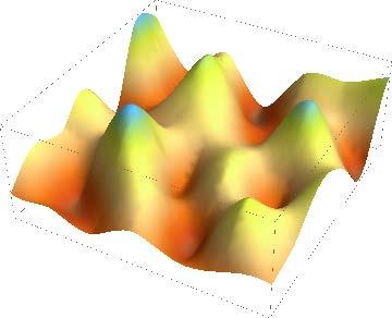
8 ( ) ( ) ( ) ( ) ( ) ( )( ) = 1 h h u u h u h u r d h h u u r d h r d t h r d H y x x y y x y y y x x x y x y y x x µ λ κ ρ Two dimensional membranes Out of plane displacements lead to changes in area h L L h L Kinetic Bending Stretching Shear Two dimensional crystaline membranes are intrinsically anharmonic
9 Thermal expansion In plane strains change the freuency of out of plane modes Binding energy Flexural phonon Grüneisen parameter Thermal expansion ω = γ = κ 1 ω 4 ω u ( λ µ ) ρ = Low T u ( λ µ ) High T κ α 3 k B κ ρ log 8πκ Y Negative thermal expansion coefficient Lattice constant


10 Substrate effects Gapped flexural modes Thermal expansion
11 Out of plane fluctuations screen the in plane elastic constants 1 h c c Yu E κ 1 log κ c c Yu T T F 1 κ δ T Y u F Y = Y 10eVA T 300K 0.05eV κ 1eV l 10A YYl κ 5 1

12 Numerical results Γ Γ L T = 4 ( λ µ ) ( λ µ ) µ T = 3 4κ ρ 1 T 3 κ ρ Theory of elasticity 1
13 The self consistent screening approximation J. Physiue, 48, 1085 (1987) 4 TY d κ κ δ ( ) ( ) ( ) ( ) ( ) ( ) ( ) ( ) ( ) ( ) ( ) ( ) ( ) ( ) = = = Σ Σ = p G G p d p I I b b b p G p P b d G G T π π = = = ( ) ( ) ( ) , u u η η µ λ κ η η Power law divergences Self consistent theory, valid in high dimensions Agrees well with numerical simulaions
14 Vacancies and flexural modes ( ω) G ρω 1 κ, = 4 Σ (, ω) Σ ( ω) T-matrix approximation n V n V log a localization length κρω κρω 4 κ ρω h h = 0 κ Σ 1 n V = ρ κ infinite mass vacancies Vacancies localize flexural modes Long wavelength flexural modes do not contribute to the screening of the elastic constants
15 geometric factor percolation 600 Defects (%) A Y K 1 R 1 0 n V ηu 1 1 c 0 n V E D (N/m) E 3D (TPa) intrinsic localization length 0 x x x10 13 Defects/cm nm 0 1 k F Fracture Force (µn) Defects (%) B 0 x10 1 4x10 1 6x10 1 3x x10 13 Defects/cm
")


")


16 Young modulus and induced strains a) a) b) 750 φ = 1.5 µm 750 φ = 1 µm E D (N/m) Strain % E D (N/m) c) d) Strain % Experiments Hydrostatic pressure. Formation of bubbles Theory
17 Graphene thermal expansion coefficient Prestress (N/m) 0,15 0,10 0,05 0,00 Membrane 1 Membrane Pristine Irradiated Prestress (N/m) 0,0 0,15 0,10 0,05 Pristine Irradiated Temperature (ºC) Temperature (ºC) Thermal Expansion Coefficient: Pristine: -9.4 x 10⁻⁶ K -1 Irradiated (L D ~ 5.5 nm): -1 x 10⁻⁶ K - 1 Thermal Expansion Coefficient: Pristine: -6. x 10-6 K -1 Irradiated (L D ~ 5 nm): -1.1 x 10⁻⁶ K -1 L D : Mean distance between defects as measured by Raman


18 Electron-phonon coupling Ripples induced by electrons Charge puddles induced by strains
19 GRAPHENE S SUPERLATIVES Thinnest imaginable material largest surface area (~,700 m per gram) strongest material ever measured (theoretical limit) stiffest known material (stiffer than diamond) most stretchable crystal (up to 0% elastically) record thermal conductivity (outperforming diamond) highest current density at room T (106 times of copper) completely impermeable (even He atoms cannot sueeze through) highest intrinsic mobility (100 times more than in Si) conducts electricity in the limit of no electrons lightest charge carriers (zero rest mass) longest mean free path at room T (micron range)


20 Strains and conductivity in graphene ArXiv: , Phys. Rev. X, in press DC transport on graphene on BN High mobility samples Multiterminal devices Magnetoresistance: Scattering due to intravalley processes
21 Puddles and mobility DC transport: mobility (roughly) independent of carrier concentration DC transport: correlation between mobility and puddles Weak localization: long range scatterers Mobility vs puddle density Correlation independent of sample characteristics Long range scattering mechanisms: Coulomb impurities Strains


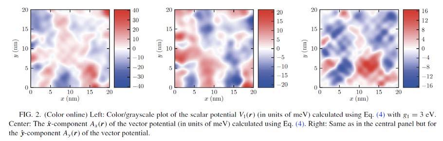
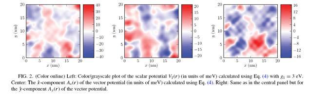
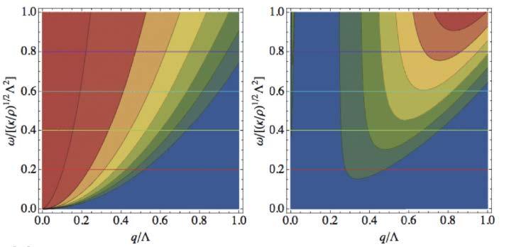
22 Strains induce scalar and vector potentials

23 Relaxation times, mobilities, and puddles τ 1 = τ s 1 τ g 1 τ 1 s π N ε F ħ 4π τ g 1 π ħ N ε F π μ = σ nn = e h dd 1 cos θ 0 π v F k F τ nn V s V s ε =k F sin θ 4π dd 1 cos θ A A =kf sin θ 0

24 Wrinkles and transport Strains: Supress either weak localization, or weak antilocalization. Lead to long range, intravalley scattering. Induce puddles near the neutrality point. Corrugations induce scalar and gauge potentials


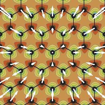
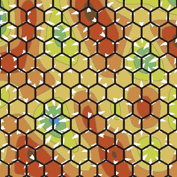
25 Substrate induced random forces


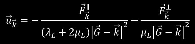
26 1 μn ħ e 1 4 log Λ k F 1 16α g g 1 1 λ L μ L μ L g ev

27 Bilayer graphene

28 Raman measurements: Correlations between strains and mobilities in graphene on BN


29 Anharmonic properties of graphene Anharmonic effects in membranes Negative thermal expansion coefficient Screening of the in plane stiffness The elastic response of graphene depends on the experimental setup (size, temperature, defects, pre existing strain, ) arxiv: Universal properties of transport in graphene Scattering is due to intravalley processes Interference processes (weak localization) are suppressed Puddles and transport are correlated Strains are the most likely origin of puddles and scattering ArXiv: , Phys. Rev. X, in press

 3 associated partners")
30 ITN= Initial Training Network Marie Curie Program TOPIC:Spintronics in graphene Lifespan: Sep. 013 Aug 017 Groups: 9 partners (CSIC; CNRS, Manchester, Groningen, Aachen, INL, Nanogune, Graphenea, AMO) 3 associated partners #Trainees: 11 Phd students, 4 postdocs Coordinated by 30
Motivation. Confined acoustics phonons. Modification of phonon lifetimes Antisymmetric Bulk. Symmetric. 10 nm
 Motivation Confined acoustics phonons Modification of phonon lifetimes 0 0 Symmetric Antisymmetric Bulk 0 nm A. Balandin et al, PRB 58(998) 544 Effect of native oxide on dispersion relation Heat transport
Graphene-reinforced elastomers for demanding environments
 Graphene-reinforced elastomers for demanding environments Robert J Young, Ian A. Kinloch, Dimitrios G. Papageorgiou, J. Robert Innes and Suhao Li School of Materials and National Graphene Institute The
STM and graphene. W. W. Larry Pai ( 白偉武 ) Center for condensed matter sciences, National Taiwan University NTHU, 2013/05/23
 Center for condensed matter sciences, National Taiwan University NTHU, 2013/05/23") STM and graphene W. W. Larry Pai ( 白偉武 ) Center for condensed matter sciences, National Taiwan University NTHU, 2013/05/23 Why graphene is important: It is a new form of material (two dimensional, single
STM and graphene W. W. Larry Pai ( 白偉武 ) Center for condensed matter sciences, National Taiwan University NTHU, 2013/05/23 Why graphene is important: It is a new form of material (two dimensional, single
CVD growth of Graphene. SPE ACCE presentation Carter Kittrell James M. Tour group September 9 to 11, 2014
 CVD growth of Graphene SPE ACCE presentation Carter Kittrell James M. Tour group September 9 to 11, 2014 Graphene zigzag armchair History 1500: Pencil-Is it made of lead? 1789: Graphite 1987: The first
ECE 656 Exam 2: Fall 2013 September 23, 2013 Mark Lundstrom Purdue University (Revised 9/25/13)
") NAME: PUID: : ECE 656 Exam : September 3, 03 Mark Lundstrom Purdue University (Revised 9/5/3) This is a closed book exam. You may use a calculator and the formula sheet at the end of this exam. There are
NAME: PUID: : ECE 656 Exam : September 3, 03 Mark Lundstrom Purdue University (Revised 9/5/3) This is a closed book exam. You may use a calculator and the formula sheet at the end of this exam. There are
Lecture 11 - Phonons II - Thermal Prop. Continued
 Phonons II - hermal Properties - Continued (Kittel Ch. 5) Low High Outline Anharmonicity Crucial for hermal expansion other changes with pressure temperature Gruneisen Constant hermal Heat ransport Phonon
height trace of a 2L BN mechanically exfoliated on SiO 2 /Si with pre-fabricated micro-wells. Scale bar 2 µm.
 Supplementary Figure 1. Few-layer BN nanosheets. AFM image and the corresponding height trace of a 2L BN mechanically exfoliated on SiO 2 /Si with pre-fabricated micro-wells. Scale bar 2 µm. Supplementary
Lecture 22: Ionized Impurity Scattering
 ECE-656: Fall 20 Lecture 22: Ionized Impurity Scattering Mark Lundstrom Purdue University West Lafayette, IN USA 0/9/ scattering of plane waves ψ i = Ω ei p r U S ( r,t) incident plane wave ( ) = 2π H
Rippling and Ripping Graphene
 Rippling and Ripping Graphene Michael Marder Professor of Physics Center for Nonlinear Dynamics and Department of Physics The University of Texas at Austin Clifton Symposium, June 2012, Symi Marder (UT
Intensity (a.u.) Intensity (a.u.) Raman Shift (cm -1 ) Oxygen plasma. 6 cm. 9 cm. 1mm. Single-layer graphene sheet. 10mm. 14 cm
 Intensity (a.u.) Raman Shift (cm -1 ) Oxygen plasma. 6 cm. 9 cm. 1mm. Single-layer graphene sheet. 10mm. 14 cm") Intensity (a.u.) Intensity (a.u.) a Oxygen plasma b 6 cm 1mm 10mm Single-layer graphene sheet 14 cm 9 cm Flipped Si/SiO 2 Patterned chip Plasma-cleaned glass slides c d After 1 sec normal Oxygen plasma
Intensity (a.u.) Intensity (a.u.) a Oxygen plasma b 6 cm 1mm 10mm Single-layer graphene sheet 14 cm 9 cm Flipped Si/SiO 2 Patterned chip Plasma-cleaned glass slides c d After 1 sec normal Oxygen plasma
Solid State Device Fundamentals
 Solid State Device Fundamentals ENS 345 Lecture Course by Alexander M. Zaitsev alexander.zaitsev@csi.cuny.edu Tel: 718 982 2812 Office 4N101b 1 Outline - Goals of the course. What is electronic device?
Electrical Resistance
 Electrical Resistance I + V _ W Material with resistivity ρ t L Resistance R V I = L ρ Wt (Unit: ohms) where ρ is the electrical resistivity 1 Adding parts/billion to parts/thousand of dopants to pure
Supporting Information
 Electronic Supplementary Material (ESI) for Nanoscale. This journal is The Royal Society of Chemistry 2015 Supporting Information Single Layer Lead Iodide: Computational Exploration of Structural, Electronic
Nonlinear Mechanics of Monolayer Graphene Rui Huang
 Nonlinear Mechanics of Monolayer Graphene Rui Huang Center for Mechanics of Solids, Structures and Materials Department of Aerospace Engineering and Engineering Mechanics The University of Texas at Austin
Supplementary Figure 1 Experimental setup for crystal growth. Schematic drawing of the experimental setup for C 8 -BTBT crystal growth.
 Supplementary Figure 1 Experimental setup for crystal growth. Schematic drawing of the experimental setup for C 8 -BTBT crystal growth. Supplementary Figure 2 AFM study of the C 8 -BTBT crystal growth
Chap. 11 Semiconductor Diodes
 Chap. 11 Semiconductor Diodes Semiconductor diodes provide the best resolution for energy measurements, silicon based devices are generally used for charged-particles, germanium for photons. Scintillators
Supplementary information for Tunneling Spectroscopy of Graphene-Boron Nitride Heterostructures
 Supplementary information for Tunneling Spectroscopy of Graphene-Boron Nitride Heterostructures F. Amet, 1 J. R. Williams, 2 A. G. F. Garcia, 2 M. Yankowitz, 2 K.Watanabe, 3 T.Taniguchi, 3 and D. Goldhaber-Gordon
Supplementary Information: Supplementary Figure 1. Resistance dependence on pressure in the semiconducting region.
 Supplementary Information: Supplementary Figure 1. Resistance dependence on pressure in the semiconducting region. The pressure activated carrier transport model shows good agreement with the experimental
Band-like transport in highly crystalline graphene films from
 Supplementary figures Title: Band-like transport in highly crystalline graphene films from defective graphene oxides R. Negishi 1,*, M. Akabori 2, T. Ito 3, Y. Watanabe 4 and Y. Kobayashi 1 1 Department
Thermoelectrics: A theoretical approach to the search for better materials
 Thermoelectrics: A theoretical approach to the search for better materials Jorge O. Sofo Department of Physics, Department of Materials Science and Engineering, and Materials Research Institute Penn State
chiral m = n Armchair m = 0 or n = 0 Zigzag m n Chiral Three major categories of nanotube structures can be identified based on the values of m and n
 zigzag armchair Three major categories of nanotube structures can be identified based on the values of m and n m = n Armchair m = 0 or n = 0 Zigzag m n Chiral Nature 391, 59, (1998) chiral J. Tersoff,
Outline. Introduction: graphene. Adsorption on graphene: - Chemisorption - Physisorption. Summary
 Outline Introduction: graphene Adsorption on graphene: - Chemisorption - Physisorption Summary 1 Electronic band structure: Electronic properties K Γ M v F = 10 6 ms -1 = c/300 massless Dirac particles!
6.5 mm. ε = 1%, r = 9.4 mm. ε = 3%, r = 3.1 mm
 Supplementary Information Supplementary Figures Gold wires Substrate Compression holder 6.5 mm Supplementary Figure 1 Picture of the compression holder. 6.5 mm ε = 0% ε = 1%, r = 9.4 mm ε = 2%, r = 4.7
KAVLI v F. Curved graphene revisited. María A. H. Vozmediano. Instituto de Ciencia de Materiales de Madrid CSIC
 KAVLI 2012 v F Curved graphene revisited María A. H. Vozmediano Instituto de Ciencia de Materiales de Madrid CSIC Collaborators ICMM(Graphene group) http://www.icmm.csic.es/gtg/ A. Cano E. V. Castro J.
Carbon based Nanoscale Electronics
 Carbon based Nanoscale Electronics 09 02 200802 2008 ME class Outline driving force for the carbon nanomaterial electronic properties of fullerene exploration of electronic carbon nanotube gold rush of
Center for Integrated Nanostructure Physics (CINAP)
") Center for Integrated Nanostructure Physics (CINAP) - Institute for Basic Science (IBS) was launched in 2012 by the Korean government to promote basic science in Korea - Our Center was established in 2012
Center for Integrated Nanostructure Physics (CINAP) - Institute for Basic Science (IBS) was launched in 2012 by the Korean government to promote basic science in Korea - Our Center was established in 2012
7. FREE ELECTRON THEORY.
 7. FREE ELECTRON THEORY. Aim: To introduce the free electron model for the physical properties of metals. It is the simplest theory for these materials, but still gives a very good description of many
Microscopic Ohm s Law
 Microscopic Ohm s Law Outline Semiconductor Review Electron Scattering and Effective Mass Microscopic Derivation of Ohm s Law 1 TRUE / FALSE 1. Judging from the filled bands, material A is an insulator.
Session V: Graphene. Matteo Bruna CAMBRIDGE UNIVERSITY DEPARTMENT OF ENGINEERING
 Session V: Graphene Matteo Bruna Graphene: Material in the Flatland Graphite Graphene Properties: Thinnest imaginable material Good(and tunable) electrical conductor Strongest ever measured Stiffest known
Solid State Physics II Lattice Dynamics and Heat Capacity
 SEOUL NATIONAL UNIVERSITY SCHOOL OF PHYSICS http://phya.snu.ac.kr/ ssphy2/ SPRING SEMESTER 2004 Chapter 3 Solid State Physics II Lattice Dynamics and Heat Capacity Jaejun Yu jyu@snu.ac.kr http://phya.snu.ac.kr/
Shear Properties and Wrinkling Behaviors of Finite Sized Graphene
 Shear Properties and Wrinkling Behaviors of Finite Sized Graphene Kyoungmin Min, Namjung Kim and Ravi Bhadauria May 10, 2010 Abstract In this project, we investigate the shear properties of finite sized
Heat conduction and phonon localization in disordered harmonic lattices
 Heat conduction and phonon localization in disordered harmonic lattices Anupam Kundu Abhishek Chaudhuri Dibyendu Roy Abhishek Dhar Joel Lebowitz Herbert Spohn Raman Research Institute NUS, Singapore February
Density of states for electrons and holes. Distribution function. Conduction and valence bands
 Intrinsic Semiconductors In the field of semiconductors electrons and holes are usually referred to as free carriers, or simply carriers, because it is these particles which are responsible for carrying
More Examples Of Generalized Coordinates
 Slides of ecture 8 Today s Class: Review Of Homework From ecture 7 Hamilton s Principle More Examples Of Generalized Coordinates Calculating Generalized Forces Via Virtual Work /3/98 /home/djsegal/unm/vibcourse/slides/ecture8.frm
arxiv: v1 [cond-mat.mtrl-sci] 13 Apr 2007
![arxiv: v1 [cond-mat.mtrl-sci] 13 Apr 2007](/thumbs/76/73757643.jpg "arxiv: v1 [cond-mat.mtrl-sci] 13 Apr 2007") Intrinsic ripples in graphene A. Fasolino, J. H. Los and M. I. Katsnelson Institute for Molecules and Materials, Radboud University Nijmegen, 6525 ED Nijmegen, The Netherlands arxiv:0704.1793v1 [cond-mat.mtrl-sci]
Intrinsic ripples in graphene A. Fasolino, J. H. Los and M. I. Katsnelson Institute for Molecules and Materials, Radboud University Nijmegen, 6525 ED Nijmegen, The Netherlands arxiv:0704.1793v1 [cond-mat.mtrl-sci]
collisions of electrons. In semiconductor, in certain temperature ranges the conductivity increases rapidly by increasing temperature
 1.9. Temperature Dependence of Semiconductor Conductivity Such dependence is one most important in semiconductor. In metals, Conductivity decreases by increasing temperature due to greater frequency of
ELECTRONIC TRANSPORT IN GRAPHENE
 ELECTRONIC TRANSPORT IN GRAPHENE J. González Instituto de Estructura de la Materia, CSIC, Spain 1985 1991 4 ELECTRONIC TRANSPORT IN GRAPHENE Graphene has opened the way to understand the behaior of an
FYS Vår 2017 (Kondenserte fasers fysikk)
") FYS3410 - Vår 2017 (Kondenserte fasers fysikk) http://www.uio.no/studier/emner/matnat/fys/fys3410/v16/index.html Pensum: Introduction to Solid State Physics by Charles Kittel (Chapters 1-9, 11, 17, 18,
FYS3410 - Vår 2017 (Kondenserte fasers fysikk) http://www.uio.no/studier/emner/matnat/fys/fys3410/v16/index.html Pensum: Introduction to Solid State Physics by Charles Kittel (Chapters 1-9, 11, 17, 18,
Bending Load & Calibration Module
 Bending Load & Calibration Module Objectives After completing this module, students shall be able to: 1) Conduct laboratory work to validate beam bending stress equations. 2) Develop an understanding of
EE 527 MICROFABRICATION. Lecture 5 Tai-Chang Chen University of Washington
 EE 527 MICROFABRICATION Lecture 5 Tai-Chang Chen University of Washington MICROSCOPY AND VISUALIZATION Electron microscope, transmission electron microscope Resolution: atomic imaging Use: lattice spacing.
V, I, R measurements: how to generate and measure quantities and then how to get data (resistivity, magnetoresistance, Hall). Makariy A.
. Makariy A.") V, I, R measurements: how to generate and measure quantities and then how to get data (resistivity, magnetoresistance, Hall). 590B Makariy A. Tanatar November 12, 2008 Resistivity Typical resistivity temperature
V, I, R measurements: how to generate and measure quantities and then how to get data (resistivity, magnetoresistance, Hall). 590B Makariy A. Tanatar November 12, 2008 Resistivity Typical resistivity temperature
MECHANICS OF 2D MATERIALS
 MECHANICS OF 2D MATERIALS Nicola Pugno Cambridge February 23 rd, 2015 2 Outline Stretching Stress Strain Stress-Strain curve Mechanical Properties Young s modulus Strength Ultimate strain Toughness modulus
Mechanical properties of graphene
 Costas GALIOTIS Mechanical properties of graphene BSc in Chemistry University of Athens PhD in Materials Science- University of London, Director of the Institute of Chemical Engineering and High Temperature
Transport through Andreev Bound States in a Superconductor-Quantum Dot-Graphene System
 Transport through Andreev Bound States in a Superconductor-Quantum Dot-Graphene System Nadya Mason Travis Dirk, Yung-Fu Chen, Cesar Chialvo Taylor Hughes, Siddhartha Lal, Bruno Uchoa Paul Goldbart University
Supplementary Figure 1 Magneto-transmission spectra of graphene/h-bn sample 2 and Landau level transition energies of three other samples.
 Supplementary Figure 1 Magneto-transmission spectra of graphene/h-bn sample 2 and Landau level transition energies of three other samples. (a,b) Magneto-transmission ratio spectra T(B)/T(B 0 ) of graphene/h-bn
Quantum Confinement in Graphene
 Quantum Confinement in Graphene from quasi-localization to chaotic billards MMM dominikus kölbl 13.10.08 1 / 27 Outline some facts about graphene quasibound states in graphene numerical calculation of
Thermal Transport in Graphene and other Two-Dimensional Systems. Li Shi. Department of Mechanical Engineering & Texas Materials Institute
 Thermal Transport in Graphene and other Two-Dimensional Systems Li Shi Department of Mechanical Engineering & Texas Materials Institute Outline Thermal Transport Theories and Simulations of Graphene Raman
6.730 Physics for Solid State Applications
 6.730 Physics for Solid State Applications Lecture 29: Electron-phonon Scattering Outline Bloch Electron Scattering Deformation Potential Scattering LCAO Estimation of Deformation Potential Matrix Element
Giant Intrinsic Carrier Mobilities in Graphene and Its Bilayer
 Giant Intrinsic Carrier Mobilities in Graphene and Its Bilayer S.V. Morozov 1,, K.S. Novoselov 1, M.I. Katsnelson, F. Schedin 1, D.C. Elias 1, J.A. Jaszczak, A.K. Geim 1 1 Manchester Centre for Mesoscience
8.1 Drift diffusion model
 8.1 Drift diffusion model Advanced theory 1 Basic Semiconductor Equations The fundamentals of semiconductor physic are well described by tools of quantum mechanic. This point of view gives us a model of
Hydrogenated Graphene
 Hydrogenated Graphene Stefan Heun NEST, Istituto Nanoscienze-CNR and Scuola Normale Superiore Pisa, Italy Outline Epitaxial Graphene Hydrogen Chemisorbed on Graphene Hydrogen-Intercalated Graphene Outline
Joint ICTP-IAEA Workshop on Physics of Radiation Effect and its Simulation for Non-Metallic Condensed Matter.
 2359-3 Joint ICTP-IAEA Workshop on Physics of Radiation Effect and its Simulation for Non-Metallic Condensed Matter 13-24 August 2012 Electrically active defects in semiconductors induced by radiation
Semiclassical formulation
 The story so far: Transport coefficients relate current densities and electric fields (currents and voltages). Can define differential transport coefficients + mobility. Drude picture: treat electrons
characterization in solids
 Electrical methods for the defect characterization in solids 1. Electrical residual resistivity in metals 2. Hall effect in semiconductors 3. Deep Level Transient Spectroscopy - DLTS Electrical conductivity
Deforming Single and Multilayer Graphenes in Tension and Compression
 Deforming Single and Multilayer Graphenes in Tension and Compression Costas Galio*s*, Georgia Tsoukleri, Konstan*nos Papagelis, John Parthenios Otakar Frank Kostya Novoselov FORTH/ICE- HT & Univ. Patras,
Electronic structure and properties of a few-layer black phosphorus Mikhail Katsnelson
 Electronic structure and properties of a few-layer black phosphorus Mikhail Katsnelson Main collaborators: Sasha Rudenko Shengjun Yuan Rafa Roldan Milton Pereira Sergey Brener Motivation Plenty of 2D materials
Frictional characteristics of exfoliated and epitaxial graphene
 Frictional characteristics of exfoliated and epitaxial graphene Young Jun Shin a,b, Ryan Stromberg c, Rick Nay c, Han Huang d, Andrew T. S. Wee d, Hyunsoo Yang a,b,*, Charanjit S. Bhatia a a Department
Quiz #1 Practice Problem Set
 Name: Student Number: ELEC 3908 Physical Electronics Quiz #1 Practice Problem Set? Minutes January 22, 2016 - No aids except a non-programmable calculator - All questions must be answered - All questions
Lecture 1. OUTLINE Basic Semiconductor Physics. Reading: Chapter 2.1. Semiconductors Intrinsic (undoped) silicon Doping Carrier concentrations
 silicon Doping Carrier concentrations") Lecture 1 OUTLINE Basic Semiconductor Physics Semiconductors Intrinsic (undoped) silicon Doping Carrier concentrations Reading: Chapter 2.1 EE105 Fall 2007 Lecture 1, Slide 1 What is a Semiconductor? Low
Lecture 1 OUTLINE Basic Semiconductor Physics Semiconductors Intrinsic (undoped) silicon Doping Carrier concentrations Reading: Chapter 2.1 EE105 Fall 2007 Lecture 1, Slide 1 What is a Semiconductor? Low
Electron-phonon scattering (Finish Lundstrom Chapter 2)
") Electron-phonon scattering (Finish Lundstrom Chapter ) Deformation potentials The mechanism of electron-phonon coupling is treated as a perturbation of the band energies due to the lattice vibration. Equilibrium
Electron-phonon scattering (Finish Lundstrom Chapter ) Deformation potentials The mechanism of electron-phonon coupling is treated as a perturbation of the band energies due to the lattice vibration. Equilibrium
Introduction to Waves in Structures. Mike Brennan UNESP, Ilha Solteira São Paulo Brazil
 Introduction to Waves in Structures Mike Brennan UNESP, Ilha Solteira São Paulo Brazil Waves in Structures Characteristics of wave motion Structural waves String Rod Beam Phase speed, group velocity Low
Fe 1-x Co x Si, a Silicon Based Magnetic Semiconductor
 Fe 1-x Co x Si, a Silicon Based Magnetic Semiconductor T (K) 1 5 Fe.8 Co.2 Si ρ xy (µω cm) J.F. DiTusa N. Manyala LSU Y. Sidis D.P. Young G. Aeppli UCL Z. Fisk FSU T C 1 Nature Materials 3, 255-262 (24)
FMM, 15 th Feb Simon Zihlmann
 FMM, 15 th Feb. 2013 Simon Zihlmann Outline Motivation Basics about graphene lattice and edges Introduction to Raman spectroscopy Scattering at the edge Polarization dependence Thermal rearrangement of
Nonlinear Electrodynamics and Optics of Graphene
 Nonlinear Electrodynamics and Optics of Graphene S. A. Mikhailov and N. A. Savostianova University of Augsburg, Institute of Physics, Universitätsstr. 1, 86159 Augsburg, Germany E-mail: sergey.mikhailov@physik.uni-augsburg.de
Molecular Dynamics Simulation of Fracture of Graphene
 Molecular Dynamics Simulation of Fracture of Graphene Dewapriya M. A. N. 1, Rajapakse R. K. N. D. 1,*, Srikantha Phani A. 2 1 School of Engineering Science, Simon Fraser University, Burnaby, BC, Canada
Growth of Graphene Architectures on SiC
 Wright State University CORE Scholar Special Session 5: Carbon and Oxide Based Nanostructured Materials (2012) Special Session 5 6-2012 Growth of Graphene Architectures on SiC John J. Boeckl Weijie Lu
N = N A Pb A Pb. = ln N Q v kt. = kt ln v N
 5. Calculate the energy for vacancy formation in silver, given that the equilibrium number of vacancies at 800 C (1073 K) is 3.6 10 3 m 3. The atomic weight and density (at 800 C) for silver are, respectively,
Non-traditional methods of material properties and defect parameters measurement
 Non-traditional methods of material properties and defect parameters measurement Juozas Vaitkus on behalf of a few Vilnius groups Vilnius University, Lithuania Outline: Definition of aims Photoconductivity
3.032 Problem Set 2 Solutions Fall 2007 Due: Start of Lecture,
 3.032 Problem Set 2 Solutions Fall 2007 Due: Start of Lecture, 09.21.07 1. In the beam considered in PS1, steel beams carried the distributed weight of the rooms above. To reduce stress on the beam, it
Thermal Stress and Strain in a GaN Epitaxial Layer Grown on a Sapphire Substrate by the MOCVD Method
 CHINESE JOURNAL OF PHYSICS VOL. 48, NO. 3 June 2010 Thermal Stress and Strain in a GaN Epitaxial Layer Grown on a Sapphire Substrate by the MOCVD Method H. R. Alaei, 1 H. Eshghi, 2 R. Riedel, 3 and D.
Luttinger Liquid at the Edge of a Graphene Vacuum
 Luttinger Liquid at the Edge of a Graphene Vacuum H.A. Fertig, Indiana University Luis Brey, CSIC, Madrid I. Introduction: Graphene Edge States (Non-Interacting) II. III. Quantum Hall Ferromagnetism and
Review of Electromechanical Concepts
 Review of Electromechanical Concepts Part I Electrical properties p of semiconductors Free charge carriers in silicon Energy bands of insulators, semiconductors, and metals Charge carrier concentration
TOPOLOGICAL BANDS IN GRAPHENE SUPERLATTICES
 TOPOLOGICAL BANDS IN GRAPHENE SUPERLATTICES 1) Berry curvature in superlattice bands 2) Energy scales for Moire superlattices 3) Spin-Hall effect in graphene Leonid Levitov (MIT) @ ISSP U Tokyo MIT Manchester
Omnidirectionally Stretchable and Transparent Graphene Electrodes
 Supporting Information for: Omnidirectionally Stretchable and Transparent Graphene Electrodes Jin Yong Hong,, Wook Kim, Dukhyun Choi, Jing Kong,*, and Ho Seok Park*, School of Chemical Engineering, Sungkyunkwan
R measurements (resistivity, magnetoresistance, Hall). Makariy A. Tanatar
. Makariy A. Tanatar") R measurements (resistivity, magnetoresistance, Hall). 590B Makariy A. Tanatar April 18, 2014 Resistivity Typical resistivity temperature dependence: metals, semiconductors Magnetic scattering Resistivities
R measurements (resistivity, magnetoresistance, Hall). 590B Makariy A. Tanatar April 18, 2014 Resistivity Typical resistivity temperature dependence: metals, semiconductors Magnetic scattering Resistivities
Semiconductor Device Physics
 1 Semiconductor Device Physics Lecture 3 http://zitompul.wordpress.com 2 0 1 3 Semiconductor Device Physics 2 Three primary types of carrier action occur inside a semiconductor: Drift: charged particle
Supplementary material for High responsivity mid-infrared graphene detectors with antenna-enhanced photo-carrier generation and collection
 Supplementary material for High responsivity mid-infrared graphene detectors with antenna-enhanced photo-carrier generation and collection Yu Yao 1, Raji Shankar 1, Patrick Rauter 1, Yi Song 2, Jing Kong
Solid State Theory Physics 545
 olid tate Theory hysics 545 Mechanical properties of materials. Basics. tress and strain. Basic definitions. Normal and hear stresses. Elastic constants. tress tensor. Young modulus. rystal symmetry and
Solid State Device Fundamentals
 Solid State Device Fundamentals ENS 345 Lecture Course by Alexander M. Zaitsev alexander.zaitsev@csi.cuny.edu Tel: 718 982 2812 Office 4N101b 1 Outline - Goals of the course. What is electronic device?
Olivier Bourgeois Institut Néel
 Olivier Bourgeois Institut Néel Outline Introduction: necessary concepts: phonons in low dimension, characteristic length Part 1: Transport and heat storage via phonons Specific heat and kinetic equation
Ferromagnetism and Anomalous Hall Effect in Graphene
 Ferromagnetism and Anomalous Hall Effect in Graphene Jing Shi Department of Physics & Astronomy, University of California, Riverside Graphene/YIG Introduction Outline Proximity induced ferromagnetism Quantized
Crystal Relaxation, Elasticity, and Lattice Dynamics
 http://exciting-code.org Crystal Relaxation, Elasticity, and Lattice Dynamics Pasquale Pavone Humboldt-Universität zu Berlin http://exciting-code.org PART I: Structure Optimization Pasquale Pavone Humboldt-Universität
Semiconductor physics I. The Crystal Structure of Solids
 Lecture 3 Semiconductor physics I The Crystal Structure of Solids 1 Semiconductor materials Types of solids Space lattices Atomic Bonding Imperfection and doping in SOLIDS 2 Semiconductor Semiconductors
Mechanics of Earthquakes and Faulting
 Mechanics of Earthquakes and Faulting Lectures & 3, 9/31 Aug 017 www.geosc.psu.edu/courses/geosc508 Discussion of Handin, JGR, 1969 and Chapter 1 Scholz, 00. Stress analysis and Mohr Circles Coulomb Failure
Impact of disorder and topology in two dimensional systems at low carrier densities
 Impact of disorder and topology in two dimensional systems at low carrier densities A Thesis Submitted For the Degree of Doctor of Philosophy in the Faculty of Science by Mohammed Ali Aamir Department
Phase Transitions in Strontium Titanate
 Phase Transitions in Strontium Titanate Xinyue Fang Department of Physics, University of Illinois at Urbana-Champaign Abstract Strontium Titanate SrTiO 3 (STO) is known to undergo an antiferrodistortive
Luminescence basics. Slide # 1
 Luminescence basics Types of luminescence Cathodoluminescence: Luminescence due to recombination of EHPs created by energetic electrons. Example: CL mapping system Photoluminescence: Luminescence due to
EE C247B / ME C218 INTRODUCTION TO MEMS DESIGN SPRING 2016 C. NGUYEN PROBLEM SET #4
 Issued: Wednesday, March 4, 2016 PROBLEM SET #4 Due: Monday, March 14, 2016, 8:00 a.m. in the EE C247B homework box near 125 Cory. 1. This problem considers bending of a simple cantilever and several methods
Spin Orbit Coupling (SOC) in Graphene
 in Graphene") Spin Orbit Coupling (SOC) in Graphene MMM, Mirko Rehmann, 12.10.2015 Motivation Weak intrinsic SOC in graphene: [84]: Phys. Rev. B 80, 235431 (2009) [85]: Phys. Rev. B 82, 125424 (2010) [86]: Phys. Rev.
Spin Orbit Coupling (SOC) in Graphene MMM, Mirko Rehmann, 12.10.2015 Motivation Weak intrinsic SOC in graphene: [84]: Phys. Rev. B 80, 235431 (2009) [85]: Phys. Rev. B 82, 125424 (2010) [86]: Phys. Rev.
Inelastic X ray Scattering
 Inelastic X ray Scattering with mev energy resolution Tullio Scopigno University of Rome La Sapienza INFM - Center for Complex Dynamics in Structured Systems Theoretical background: the scattering cross
Coherent control and TLS-mediated damping of SiN nanoresonators. Eva Weig
 Coherent control and TLS-mediated damping of SiN nanoresonators Eva Weig Doubly-clamped pre-stressed silicon nitride string as Megahertz nanomechanical resonator fundamental flexural mode (in-plane) ~
Spring 2005 MSE111 Midterm. Prof. Eugene Haller. 3/15/05, 9:40 am
 Spring 005 MSE111 Midterm Prof. Eugene Haller 3/15/05, 9:40 am University of California at Berkeley Department of Materials Science and Engineering 80 minutes, 68 points total, 10 pages Name: SID: Problem
SUPPLEMENTARY INFORMATION
 1. Supplementary Methods Characterization of AFM resolution We employed amplitude-modulation AFM in non-contact mode to characterize the topography of the graphene samples. The measurements were performed
PG5295 Muitos Corpos 1 Electronic Transport in Quantum dots 2 Kondo effect: Intro/theory. 3 Kondo effect in nanostructures
 PG5295 Muitos Corpos 1 Electronic Transport in Quantum dots 2 Kondo effect: Intro/theory. 3 Kondo effect in nanostructures Prof. Luis Gregório Dias DFMT PG5295 Muitos Corpos 1 Electronic Transport in Quantum
Supplementary Information
 Supplementary Information Ballistic Thermal Transport in Carbyne and Cumulene with Micron-Scale Spectral Acoustic Phonon Mean Free Path Mingchao Wang and Shangchao Lin * Department of Mechanical Engineering,
Graphene. Tianyu Ye November 30th, 2011
 Graphene Tianyu Ye November 30th, 2011 Outline What is graphene? How to make graphene? (Exfoliation, Epitaxial, CVD) Is it graphene? (Identification methods) Transport properties; Other properties; Applications;
THE UNIVERSITY OF NEW SOUTH WALES SCHOOL OF PHYSICS FINAL EXAMINATION JUNE/JULY PHYS3080 Solid State Physics
 THE UNIVERSITY OF NEW SOUTH WALES SCHOOL OF PHYSICS FINAL EXAMINATION JUNE/JULY 006 PHYS3080 Solid State Physics Time Allowed hours Total number of questions - 5 Answer ALL questions All questions are
S1. X-ray photoelectron spectroscopy (XPS) survey spectrum of
 survey spectrum of") Site-selective local fluorination of graphene induced by focused ion beam irradiation Hu Li 1, Lakshya Daukiya 2, Soumyajyoti Haldar 3, Andreas Lindblad 4, Biplab Sanyal 3, Olle Eriksson 3, Dominique Aubel
Site-selective local fluorination of graphene induced by focused ion beam irradiation Hu Li 1, Lakshya Daukiya 2, Soumyajyoti Haldar 3, Andreas Lindblad 4, Biplab Sanyal 3, Olle Eriksson 3, Dominique Aubel
Kinetics. Rate of change in response to thermodynamic forces
 Kinetics Rate of change in response to thermodynamic forces Deviation from local equilibrium continuous change T heat flow temperature changes µ atom flow composition changes Deviation from global equilibrium
Cytoskeleton dynamics simulation of the red blood cell
 1 Cytoskeleton dynamics simulation of the red blood cell Ju Li Collaborators: Subra Suresh, Ming Dao, George Lykotrafitis, Chwee-Teck Lim Optical tweezers stretching of healthy human red blood cell 2 Malaria