Nanoholes for leak metrology
|
|
|
- Jack Johns
- 6 years ago
- Views:
Transcription

1 Vacuum Metrology for Industry Nanoholes for leak metrology Università Degli Studi di Genova, Italy
2 OUTLINE INTRODUCTION FABRICATION OF NANOHOLES GEOMETRICAL CHARACTERIZATION LEAK DEVICES RESULTS: PTB INRIM IMT Institute of Metals and Technology
3 Nanoholes Why? The behavior of many types of leak artefacts is not predictable using only their geometry For leak artefacts working in the molecular flow regime, the conductance and the flow rates can be easily predicted from their geometry Molecular flow Kn 1 Kn = λ d Mean free path Representative physical length scale λ d d is the diameter of a circular tube
4 p=1000 mbar λ ~ 200 nm
5 Why nanoholes? The behavior of many types of leak artefacts is not predictable using only their geometry For leak artefacts working in the molecular flow regime the conductance and the flow rates can be easily predicted from their geometry Molecular flow Kn 1 Mean free path Kn = λ d λ Representative physical length scale λ d d 200 nm
 Resolution: 1 nm Scanning Transmission electron Microscopy")
 Atomic Force Microscopy (AFM).")
6 Nanotechnology: Tools and techniques The nanoholes are manufactured by: Focused Ion Beam (FIB) milling silicon nitride membrane Resolution: 7 nm The nanoholes shape are characterized by: Scanning Electron Microscopy (SEM) Resolution: 1 nm Scanning Transmission electron Microscopy (STEM) Resolution: nm Focused Ion Beam CrossBeam 1540XB by Zeiss Ultra High Resolution Field Emission SE M(UHR-FE-SEM) Atomic Force Microscopy (AFM). Resolution: Z = 0.1 nm; X-Y = tip dependent resolution Atomic Force Microscope Dimension 3100 by Digital Instruments - Veeco
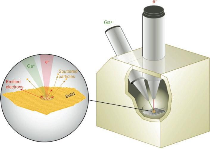


7 FABRICATION: FIB FIB SEM 5 mm Si 3 N 4 membrane 200 nm 100 nm 5 nm Si chip
 ion energy 100 nm membrane thickness 100 pa current 50 pa current Dwell time 2s Dwell time 1s Dwell time 2s Dwell time 1s Hole diameter 200 nm Hole diameter <100")
8 FIB SEM FIB PARAMETERS Ion Energy Current Dwell Time 30 kev Ga (I) ion energy 200 nm membrane thickness 200 pa current 50 pa current Dwell time 2s Dwell time 1s Dwell time 2s Dwell time 1s NO HOLE 30 kev Ga (I) ion energy 100 nm membrane thickness 100 pa current 50 pa current Dwell time 2s Dwell time 1s Dwell time 2s Dwell time 1s Hole diameter 200 nm Hole diameter <100 nm
9 Geometrical Characterization Scanning Transmission Electron Microscopy (STEM) Scanning Electron Microscopy (SEM) Atomic Force Microscopy (AFM) Focused Ion Beam (FIB)


10 SEM & STEM analysis a c OPEN AREA (nm 2 ) RADIUS (nm) b


11 AFM analysis AFM 3100 Dimension VEECO
12 WHAT ABOUT THE INNER PART?


13 a? 1? b 2 c? 3
 Electron Beam (SEM) Ion Beam (FIB) Si 3 N 4")


14 FIB Cross-section Electron Beam (SEM) 54 Ion Beam (FIB) Electron Beam (SEM) Ion Beam (FIB) Si 3 N 4 Membrane Drilling the hole with a single spot of the FIB Milling an area of the membrane with FIB close to the orifice in order to get a SEM image of the vertical walls of the hole SEM image of the cross section

15 Platinum deposition
16 Pt SiN 50 nm 150 nm Simulation of flow through the nano-hole by means of DSMC method. A modified version of the dsmcfoam solver of the OpenFOAM computational package.


17 Leak Devices

18 Nanoholes Calibration: Examples Against Vacuum He Ar N 2
19 R= 92 nm
20 R= 92 nm

")
21 Array with 48 nanoholes Nominal dimension: Average diameter D = 249 nm Length T= 100 nm Nanoholes array Mean thermal speed K. Jousten, Handbook of Vacuum Technology, Wiley-VCH (2008) Helium Calculated conductance L/s
22 Helium Measured Conductance L/s

23 Array of nano-holes calibrated against atmosphere
24 Array of nano-holes calibrated against atmosphere He N 2 Ar R134
25
 D=156 nm D=179 nm Institute of Metals and")

26 Array of 6 nanoholes calibrated against vacuum (IMT) D=156 nm D=179 nm Institute of Metals and Technology D=201 nm Length 100 nm D=165 nm D=198 nm D=191 nm Estimated total conductance = 4,0 E-8 L/s
27 Helium throughput and conductance Measured conductance = 4.5E-8 L/s


28 Outgassing Reference Device based on nanoholes technology A small device realized in cooperation UNGE-INRIM-IMT has been used as outgassing reference Layout Under patenting Some details about nanohole: The nanohole, obtained in a thin Si 3 N 4 membrane, was realized at Genova University by FIB. The nominal dimension of the nanohole are: Diameter = 213 nm Length = 100 nm
29 Conductance (L s -1 g 1/2 mol -1/2 ) 1,75E-08 1,70E-08 1,65E-08 1,60E-08 1,55E-08 1,50E-08 1,45E-08 1,40E-08 1,35E % He Ar 1,30E Upstream Pressure (mbar)

30 Acknowledgements This work is funded by EMRP (European Metrology Research Programme). The EMRP is jointly funded by the EMRP participating countries within EURAMET and European Union.
Binary gas mixtures expansion into vacuum. Dimitris Valougeorgis, Manuel Vargas, Steryios Naris
 Binary gas mixtures expansion into vacuum Dimitris Valougeorgis, Manuel Vargas, Steryios Naris University of Thessaly Department of Mechanical Engineering Laboratory of Transport Phenomena Pedion reos,
METROLOGY AND STANDARDIZATION FOR NANOTECHNOLOGIES
 MEROLOGY AND SANDARDIZAION FOR NANOECHNOLOGIES P.A.odua Center for Surface and Vacuum Research (CSVR), Moscow, Moscow Institute of Physics and echnology (MIP) E-mail: fgupnicpv@mail.ru Key words: nanotechnology,
Nova 600 NanoLab Dual beam Focused Ion Beam IITKanpur
 Nova 600 NanoLab Dual beam Focused Ion Beam system @ IITKanpur Dual Beam Nova 600 Nano Lab From FEI company (Dual Beam = SEM + FIB) SEM: The Electron Beam for SEM Field Emission Electron Gun Energy : 500
ORION NanoFab: An Overview of Applications. White Paper
 ORION NanoFab: An Overview of Applications White Paper ORION NanoFab: An Overview of Applications Author: Dr. Bipin Singh Carl Zeiss NTS, LLC, USA Date: September 2012 Introduction With the advancement
Gaetano L Episcopo. Scanning Electron Microscopy Focus Ion Beam and. Pulsed Plasma Deposition
 Gaetano L Episcopo Scanning Electron Microscopy Focus Ion Beam and Pulsed Plasma Deposition Hystorical background Scientific discoveries 1897: J. Thomson discovers the electron. 1924: L. de Broglie propose
SIB61 CRYSTAL. Report Status: PU
 Final Publishable JRP Summary for SIB61 CRYSTAL Crystalline surfaces, self-assembled structures, and nano-origami as length standards in (nano)metrology Overview Nanotechnology covers materials with dimensions
Numerical modeling of the primary source in a hemi-anechoic room
 Numerical modeling of the primary source in a hemi-anechoic room R. Arina 1, K. Völkel 2 1 Politecnico di Torino, Torino, Italy 2 Physikalisch Technische Bundesanstalt, Braunschweig, Germany ABSTRACT An
Traceability of on-machine measurements under a wide range of working conditions
 Traceability of on-machine measurements under a wide range of working conditions Frank Keller, Matthias Franke, Norbert Gerwien, Lisa Groos, Christian Held, Klaus Wendt Traceable in-process dimensional
A calibration facility for automatic weather stations
 METEOROLOGICAL APPLICATIONS Meteorol. Appl. 22: 842 846 (2015) Published online 16 November 2015 in Wiley Online Library (wileyonlinelibrary.com) DOI: 10.1002/met.1514 A calibration facility for automatic
Imaging Methods: Scanning Force Microscopy (SFM / AFM)
") Imaging Methods: Scanning Force Microscopy (SFM / AFM) The atomic force microscope (AFM) probes the surface of a sample with a sharp tip, a couple of microns long and often less than 100 Å in diameter.
Imaging Methods: Scanning Force Microscopy (SFM / AFM) The atomic force microscope (AFM) probes the surface of a sample with a sharp tip, a couple of microns long and often less than 100 Å in diameter.
Revealing High Fidelity of Nanomolding Process by Extracting the Information from AFM Image with Systematic Artifacts
 Revealing High Fidelity of Nanomolding Process by Extracting the Information from AFM Image with Systematic Artifacts Sajal Biring* Department of Electronics Engineering and Organic Electronics Research
Nanometrology and its role in the development of nanotechnology
 Nanometrology and its role in the development of nanotechnology Rob Bergmans Nederlands Meetinstituut Van Swinden Laboratorium 1 NMi Van Swinden Laboratorium The Art of Measurement Dutch national metrology
Crystalline Surfaces for Laser Metrology
 Crystalline Surfaces for Laser Metrology A.V. Latyshev, Institute of Semiconductor Physics SB RAS, Novosibirsk, Russia Abstract: The number of methodological recommendations has been pronounced to describe
Numerical analysis of the spectral response of an NSOM measurement
 Birck Nanotechnology Center Birck and NCN Publications Purdue Libraries Year 2008 Numerical analysis of the spectral response of an NSOM measurement Edward C. Kinzel Xianfan Xu Purdue University, kinzele@purdue.edu
CURRENT STATUS OF NANOIMPRINT LITHOGRAPHY DEVELOPMENT IN CNMM
 U.S. -KOREA Forums on Nanotechnology 1 CURRENT STATUS OF NANOIMPRINT LITHOGRAPHY DEVELOPMENT IN CNMM February 17 th 2005 Eung-Sug Lee,Jun-Ho Jeong Korea Institute of Machinery & Materials U.S. -KOREA Forums
Conductance measurement of a conical tube and calculation of the pressure distribution
 Conductance measurement of a conical tube and calculation of the pressure distribution B. Mercier a Laboratoire de l Accélérateur Linéaire (LAL), Université Paris-Sud, Batiment 200, BP34, 9898 Orsay Cedex,
Reference nanometrology based on AFM, SEM and TEM techniques
 Reference nanometrology based on AFM, SEM and TEM techniques Abstract Gaoliang Dai, Wolfgang Häßler-Grohne, Jens Fluegge, Harald Bosse Physikalisch-Technische Bundesanstalt, 38116 Braunschweig, Germany
SUPPLEMENTARY INFORMATION
 SUPPLEMENTARY INFORMATION DOI: 10.1038/NNANO.2011.123 Ultra-strong Adhesion of Graphene Membranes Steven P. Koenig, Narasimha G. Boddeti, Martin L. Dunn, and J. Scott Bunch* Department of Mechanical Engineering,
UHV - Technology. Oswald Gröbner
 School on Synchrotron Radiation UHV - Technology Trieste, 20-21 April 2004 1) Introduction and some basics 2) Building blocks of a vacuum system 3) How to get clean ultra high vacuum 4) Desorption phenomena
Precision Cutting and Patterning of Graphene with Helium Ions. 1.School of Engineering and Applied Sciences, Harvard University, Cambridge MA 02138
 Precision Cutting and Patterning of Graphene with Helium Ions D.C. Bell 1,2, M.C. Lemme 3, L. A. Stern 4, J.R. Williams 1,3, C. M. Marcus 3 1.School of Engineering and Applied Sciences, Harvard University,
Develop and characterize a flow metering standard down to 1 nl/min
 Develop and characterize a flow metering standard down to 1 nl/min Martin Ahrens FH Lüebeck, Germany EMRP Researcher Grant HLT07- REG2 1 Project aims HLT07- REG2 develop and characterize of a flow metering
Refractive index determination of single sub micrometer vesicles in suspension using dark field microscopy
 Refractive index determination of single sub micrometer vesicles in suspension using dark field microscopy Edwin van der Pol 1,2 Frank Coumans 1,2, Anita Böing 2, Auguste Sturk 2, Rienk Nieuwland 2, and
Outlines 3/12/2011. Vacuum Chamber. Inside the sample chamber. Nano-manipulator. Focused ion beam instrument. 1. Other components of FIB instrument
 Focused ion beam instruments Outlines 1. Other components of FIB instrument 1.a Vacuum chamber 1.b Nanomanipulator 1.c Gas supply for deposition 1.d Detectors 2. Capabilities of FIB instrument Lee Chow
Determination of Minimum Detectable Partial Pressure (MDPP) of QMS and its Uncertainty
 of QMS and its Uncertainty") Workshop on Towards more reliable partial and outgassing rate measurements Berlin, Germany, January 30 - February 1, 2017 Determination of Minimum Detectable Partial Pressure (MDPP) of QMS and its Uncertainty
Workshop on Towards more reliable partial and outgassing rate measurements Berlin, Germany, January 30 - February 1, 2017 Determination of Minimum Detectable Partial Pressure (MDPP) of QMS and its Uncertainty
Electrical Characterization with SPM Application Modules
 Electrical Characterization with SPM Application Modules Metrology, Characterization, Failure Analysis: Data Storage Magnetoresistive (MR) read-write heads Semiconductor Transistors Interconnect Ferroelectric
Vapor-Phase Cutting of Carbon Nanotubes Using a Nanomanipulator Platform
 Vapor-Phase Cutting of Carbon Nanotubes Using a Nanomanipulator Platform MS&T 10, October 18, 2010 Vladimir Mancevski, President and CTO, Xidex Corporation Philip D. Rack, Professor, The University of
Simulation of Ion Beam Etching of Patterned Nanometer-scale Magnetic Structures for High-Density Storage Applications
 Engineered Excellence A Journal for Process and Device Engineers Simulation of Ion Beam Etching of Patterned Nanometer-scale Magnetic Structures for High-Density Storage Applications Introduction Fabrication
Final exam: take-home part
 Final exam: take-home part! List five things that can be done to improve this class. Be specific; give much detail.! (You will be penalized only for insulting comments made for no benefit; you will not
A simplified method of VNA uncertainty estimation
 A simplified method of VNA uncertainty estimation Markus Zeier, Johannes Hoffmann, Jurg Ruefenacht, Michael Wollensack METAS ANAMET Workshop, PTB Braunschweig, 17.12.2014 ANAMET 1 METAS Outline Introduction
Open Access Repository eprint
 Open Access Repository eprint Terms and Conditions: Users may access, download, store, search and print a hard copy of the article. Copying must be limited to making a single printed copy or electronic
Table of Content. Mechanical Removing Techniques. Ultrasonic Machining (USM) Sputtering and Focused Ion Beam Milling (FIB)
 Sputtering and Focused Ion Beam Milling (FIB)") Table of Content Mechanical Removing Techniques Ultrasonic Machining (USM) Sputtering and Focused Ion Beam Milling (FIB) Ultrasonic Machining In ultrasonic machining (USM), also called ultrasonic grinding,
Table of Content Mechanical Removing Techniques Ultrasonic Machining (USM) Sputtering and Focused Ion Beam Milling (FIB) Ultrasonic Machining In ultrasonic machining (USM), also called ultrasonic grinding,
A Sub-millikelvin Calibration Facility in the Range 0 C to 30 C
 Int J Thermophys (2017) 38:37 DOI 10.1007/s10765-016-2171-9 TEMPMEKO 2016 A Sub-millikelvin Calibration Facility in the Range 0 C to 30 C R. Bosma 1 A. Peruzzi 1 R. Van Breugel 1 C. Bruin-Barendregt 1
Integrated measuring system for MEMS
 Integrated measuring system for MEMS Thermal characterization of gas flows under slip-flow regime Alice Vittoriosi May 16, 2011 I NSTITUTE FOR M ICRO P ROCESS E NGINEERING - T HERMAL P ROCESS E NGINEERING
High Precision Dimensional Metrology of Periodic Nanostructures using Laser Scatterometry
 High Precision Dimensional Metrology of Periodic Nanostructures using Laser Scatterometry B. Bodermann, S. Bonifer, E. Buhr, A. Diener, M. Wurm, Physikalisch-Technische Bundesanstalt, Braunschweig, Germany
Analysis of shock force measurements for the model based dynamic calibration
 8 th Worshop on Analysis of Dynamic Measurements May 5-6, 4 Turin Analysis of shoc force measurements for the model based dynamic calibration Michael Kobusch, Sascha Eichstädt, Leonard Klaus, and Thomas
Supplementary Information:
 Supplementary Figures Supplementary Information: a b 1 2 3 0 ΔZ (pm) 66 Supplementary Figure 1. Xe adsorbed on a Cu(111) surface. (a) Scanning tunnelling microscopy (STM) topography of Xe layer adsorbed
Characterization and Calibration of a Fourier Transform Spectroradiometer for Solar UV Irradiance Measurements
 EMRP-ENV03 Solar UV WP 3: Improvement of Reference Spectroradiometers Characterization and Calibration of a Fourier Transform Spectroradiometer for Solar UV Irradiance Measurements Peter Meindl, Christian
Scanning Tunneling Microscopy
 Scanning Tunneling Microscopy References: 1. G. Binnig, H. Rohrer, C. Gerber, and Weibel, Phys. Rev. Lett. 49, 57 (1982); and ibid 50, 120 (1983). 2. J. Chen, Introduction to Scanning Tunneling Microscopy,
The Cylindrical Envelope Projection Model Applied to SE Images of Curved Surfaces and Comparison with AFM Evaluations
 07.80 The Microsc. Microanal. Microstruct. 513 Classification Physics Abstracts - - 06.20 61.16P The Cylindrical Envelope Projection Model Applied to SE Images of Curved Surfaces and Comparison with AFM
Final report Results and evaluation of key comparison CCM.P-K12.1 for very low helium flow rates (leak rates)
") Final report Results and evaluation of key comparison CCM.P-K1.1 for very low helium flow rates (leak rates) J. Šetina 1, M. Vičar, D. Pražák 1 Institute of Metals and Technology (IMT), Lepi pot 11, 1000
Final report Results and evaluation of key comparison CCM.P-K1.1 for very low helium flow rates (leak rates) J. Šetina 1, M. Vičar, D. Pražák 1 Institute of Metals and Technology (IMT), Lepi pot 11, 1000
Sensors and Metrology. Outline
 Sensors and Metrology A Survey 1 Outline General Issues & the SIA Roadmap Post-Process Sensing (SEM/AFM, placement) In-Process (or potential in-process) Sensors temperature (pyrometry, thermocouples, acoustic
SUPPLEMENTARY INFORMATION
 An atomically thin matter-wave beam splitter Christian Brand, Michele Sclafani, Christian Knobloch, Yigal Lilach, Thomas Juffmann, Jani Kotakoski, Clemens Mangler, Andreas Winter, Andrey Turchanin, Jannik
MEMS Metrology. Prof. Tianhong Cui ME 8254
 MEMS Metrology Prof. Tianhong Cui ME 8254 What is metrology? Metrology It is the science of weights and measures Refers primarily to the measurements of length, weight, time, etc. Mensuration- A branch
Kavli Workshop for Journalists. June 13th, CNF Cleanroom Activities
 Kavli Workshop for Journalists June 13th, 2007 CNF Cleanroom Activities Seeing nm-sized Objects with an SEM Lab experience: Scanning Electron Microscopy Equipment: Zeiss Supra 55VP Scanning electron microscopes
Supplementary Information. Large Scale Graphene Production by RF-cCVD Method
 Supplementary Information Large Scale Graphene Production by RF-cCVD Method Enkeleda Dervishi, *a,b Zhongrui Li, b Fumiya Watanabe, b Abhijit Biswas, c Yang Xu, b Alexandru R. Biris, d Viney Saini, a,b
Thermal measurements using Scanning Thermal Microscopy (SThM) Micro and Nanoscale measurements
 Micro and Nanoscale measurements") Lecture 2: Measurements with contact in heat transfer: principles, implementation and pitfalls PART 2 Thermal measurements using Scanning Thermal Microscopy (SThM) Micro and Nanoscale measurements Séverine
Lecture 2: Measurements with contact in heat transfer: principles, implementation and pitfalls PART 2 Thermal measurements using Scanning Thermal Microscopy (SThM) Micro and Nanoscale measurements Séverine
Ion Beam Sources for Neutral Beam Injectors: studies and design for components active cooling and caesium ovens
 Ion Beam Sources for Neutral Beam Injectors: studies and design for components active cooling and caesium ovens Andrea Rizzolo Consorzio RFX, Padova, Italy andrea.rizzolo@igi.cnr.it Advanced Physics Courses,
CHARACTERIZATION of NANOMATERIALS KHP
 CHARACTERIZATION of NANOMATERIALS Overview of the most common nanocharacterization techniques MAIN CHARACTERIZATION TECHNIQUES: 1.Transmission Electron Microscope (TEM) 2. Scanning Electron Microscope
Nanometer-Scale Materials Contrast Imaging with a Near-Field Microwave Microscope
 Nanometer-Scale Materials Contrast Imaging with a Near-Field Microwave Microscope Atif Imtiaz 1 and Steven M. Anlage Center for Superconductivity Research, Department of Physics, University of Maryland,
SI Broader Scope - Projects
 European Metrology Programme for Innovation and Research SI Broader Scope - Projects An overview of the funded projects from the Targeted Programme SI Broader Scope. The aim of these projects is to underpin
Chapter 9. Electron mean free path Microscopy principles of SEM, TEM, LEEM
 Chapter 9 Electron mean free path Microscopy principles of SEM, TEM, LEEM 9.1 Electron Mean Free Path 9. Scanning Electron Microscopy (SEM) -SEM design; Secondary electron imaging; Backscattered electron
Measurements, applications, and impact of the refractive index of extracellular vesicles
 Measurements, applications, and impact of the refractive index of extracellular vesicles Edwin van der Pol June 26th, 2014 Laboratory Experimental Clinical Chemistry; Biomedical Engineering and Physics,
Supporting Information
 Electronic Supplementary Material (ESI) for ChemComm. This journal is The Royal Society of Chemistry 2014 Supporting Information Controllable Atmospheric Pressure Growth of Mono-layer, Bi-layer and Tri-layer
Chapter 10. Nanometrology. Oxford University Press All rights reserved.
 Chapter 10 Nanometrology Oxford University Press 2013. All rights reserved. 1 Introduction Nanometrology is the science of measurement at the nanoscale level. Figure illustrates where nanoscale stands
Nanostrukturphysik (Nanostructure Physics)
") Nanostrukturphysik (Nanostructure Physics) Prof. Yong Lei & Dr. Yang Xu Fachgebiet 3D-Nanostrukturierung, Institut für Physik Contact: yong.lei@tu-ilmenau.de; yang.xu@tu-ilmenau.de Office: Unterpoerlitzer
Nanostrukturphysik (Nanostructure Physics) Prof. Yong Lei & Dr. Yang Xu Fachgebiet 3D-Nanostrukturierung, Institut für Physik Contact: yong.lei@tu-ilmenau.de; yang.xu@tu-ilmenau.de Office: Unterpoerlitzer
Nanopore/electrode structures for single-molecule biosensing
 Nanopore/electrode structures for single-molecule biosensing Dr Tim Albrecht Imperial College London Department of Chemistry & London Centre for Nanotechnology South Kensington Campus London t.albrecht@imperial.ac.uk
Large scale growth and characterization of atomic hexagonal boron. nitride layers
 Supporting on-line material Large scale growth and characterization of atomic hexagonal boron nitride layers Li Song, Lijie Ci, Hao Lu, Pavel B. Sorokin, Chuanhong Jin, Jie Ni, Alexander G. Kvashnin, Dmitry
Electronics Supplementary Information for. Manab Kundu, Cheuk Chi Albert Ng, Dmitri Y. Petrovykh and Lifeng Liu*
 Electronics Supplementary Information for Nickel foam supported mesoporous MnO 2 nanosheet arrays with superior lithium storage performance Manab Kundu, Cheuk Chi Albert Ng, Dmitri Y. Petrovykh and Lifeng
Sub-5 nm Patterning and Applications by Nanoimprint Lithography and Helium Ion Beam Lithography
 Sub-5 nm Patterning and Applications by Nanoimprint Lithography and Helium Ion Beam Lithography Yuanrui Li 1, Ahmed Abbas 1, Yuhan Yao 1, Yifei Wang 1, Wen-Di Li 2, Chongwu Zhou 1 and Wei Wu 1* 1 Department
Auger Electron Spectroscopy (AES) Prof. Paul K. Chu
 Prof. Paul K. Chu") Auger Electron Spectroscopy (AES) Prof. Paul K. Chu Auger Electron Spectroscopy Introduction Principles Instrumentation Qualitative analysis Quantitative analysis Depth profiling Mapping Examples The Auger
Auger Electron Spectroscopy (AES) Prof. Paul K. Chu Auger Electron Spectroscopy Introduction Principles Instrumentation Qualitative analysis Quantitative analysis Depth profiling Mapping Examples The Auger
Sensors and Metrology
 Sensors and Metrology A Survey 1 Outline General Issues & the SIA Roadmap Post-Process Sensing (SEM/AFM, placement) In-Process (or potential in-process) Sensors temperature (pyrometry, thermocouples, acoustic
SCANNING-PROBE TECHNIQUES OR APPARATUS; APPLICATIONS OF SCANNING-PROBE TECHNIQUES, e.g. SCANNING PROBE MICROSCOPY [SPM]
![SCANNING-PROBE TECHNIQUES OR APPARATUS; APPLICATIONS OF SCANNING-PROBE TECHNIQUES, e.g. SCANNING PROBE MICROSCOPY [SPM]](/thumbs/81/83165631.jpg "SCANNING-PROBE TECHNIQUES OR APPARATUS; APPLICATIONS OF SCANNING-PROBE TECHNIQUES, e.g. SCANNING PROBE MICROSCOPY [SPM]") G01Q SCANNING-PROBE TECHNIQUES OR APPARATUS; APPLICATIONS OF SCANNING-PROBE TECHNIQUES, e.g. SCANNING PROBE MICROSCOPY [SPM] Scanning probes, i.e. devices having at least a tip of nanometre sized dimensions
G01Q SCANNING-PROBE TECHNIQUES OR APPARATUS; APPLICATIONS OF SCANNING-PROBE TECHNIQUES, e.g. SCANNING PROBE MICROSCOPY [SPM] Scanning probes, i.e. devices having at least a tip of nanometre sized dimensions
Characterization of radiation quality based on nanodosimetry. Hans Rabus
 Characterization of radiation quality based on nanodosimetry Hans Rabus Physikalisch-Technische Bundesanstalt (PTB), Braunschweig, Germany Motivation Biological effectiveness of ionizing radiation depends
2D Materials Research Activities at the NEST lab in Pisa, Italy. Stefan Heun NEST, Istituto Nanoscienze-CNR and Scuola Normale Superiore, Pisa, Italy
 2D Materials Research Activities at the NEST lab in Pisa, Italy Stefan Heun NEST, Istituto Nanoscienze-CNR and Scuola Normale Superiore, Pisa, Italy 2D Materials Research Activities at the NEST lab in
THE NEW WATT BALANCE EXPERIMENT AT METAS
 XX IMEKO World Congress Metrology for Green Growth September 9 14, 2012, Busan, Republic of Korea THE NEW WATT BALANCE EXPERIMENT AT METAS H. Baumann, A. Eichenberger, B. Jeckelmann, Ch. Beguin +, R. Clavel,
User Fees for the 4D LABS Characterization Facility
 User Fees for the 4D LABS Characterization Facility 1. Imaging Fees Service SEM 1 - Helios: SEM/EDS mode SEM/EDS mode with FIB functions Cryo mode setup SEM 2 Nova NanoSEM SEM/EDS mode SEM/EDS mode with
SUPPLEMENTARY INFORMATION
 SUPPLEMENTARY INFORMATION DOI: 10.1038/NNANO.2012.162 Selective Molecular Sieving Through Porous Graphene Steven P. Koenig, Luda Wang, John Pellegrino, and J. Scott Bunch* *email: jbunch@colorado.edu Supplementary
Device Characterization of 0.21 µm CMOS Device
 Device Characterization of 0.21 µm CMOS Device Lim Teck Foo 1 *, Ibrahim Ahmad 2 and Muhammad Suhaimi Sulong 3 1 Department of Product Engineering, Altera Corporation. 2 Department of Electrical, Electronics,
Modern physics. 4. Barriers and wells. Lectures in Physics, summer
 Modern physics 4. Barriers and wells Lectures in Physics, summer 016 1 Outline 4.1. Particle motion in the presence of a potential barrier 4.. Wave functions in the presence of a potential barrier 4.3.
Dual Beam Helios Nanolab 600 and 650
 Dual Beam Helios Nanolab 600 and 650 In the Clean Room facilities of the INA LMA, several lithography facilities permit to pattern structures at the micro and nano meter scale and to create devices. In
Conventional Transmission Electron Microscopy. Introduction. Text Books. Text Books. EMSE-509 CWRU Frank Ernst
 Text Books Conventional Transmission Electron Microscopy EMSE-509 CWRU Frank Ernst D. B. Williams and C. B. Carter: Transmission Electron Microscopy, New York: Plenum Press (1996). L. Reimer: Transmission
Review of investigation of influence of operational parameters on metrological characteristics of QMS within EMRP IND12 project
 Review of investigation of influence of operational parameters on metrological characteristics of QMS within EMRP IND12 project Janez Setina Institute of Metals and Technology, (IMT), Slovenia 1 Some operational
Outline Scanning Probe Microscope (SPM)
") AFM Outline Scanning Probe Microscope (SPM) A family of microscopy forms where a sharp probe is scanned across a surface and some tip/sample interactions are monitored Scanning Tunneling Microscopy (STM)
AFM Outline Scanning Probe Microscope (SPM) A family of microscopy forms where a sharp probe is scanned across a surface and some tip/sample interactions are monitored Scanning Tunneling Microscopy (STM)
Scanning Probe Microscopy
 1 Scanning Probe Microscopy Dr. Benjamin Dwir Laboratory of Physics of Nanostructures (LPN) Benjamin.dwir@epfl.ch PH.D3.344 Outline: Introduction: What is SPM, history STM AFM Image treatment Advanced
The in-flight calibration system for the airborne imager GLORIA
 CALCON Technical Conference Utah State University, Logan, UT, USA August 4, 04 F. Olschewski, A. Ebersoldt, F. Friedl-Vallon, B. Gutschwager 4, J. Hollandt 4, A. Kleinert, C. Piesch, C. Monte 4, P. Preusse
Supplementary Information
 Supplementary Information Supplementary Figures Supplementary figure S1: Characterisation of the electron beam intensity profile. (a) A 3D plot of beam intensity (grey value) with position, (b) the beam
Influence of directivity and spectral shape on the measured sound power level
 Influence of directivity and spectral shape on the measured sound power level K. Voelkel 1, V. Wittstock Physikalisch Technische Bundesanstalt, Braunschweig, Germany ABSTRACT The sound power is the main
Accelerated Neutral Atom Beam Processing of Ultra-thin Membranes to Enhance EUV Transmittance. February 22, 2015
 Accelerated Neutral Atom Beam Processing of Ultra-thin Membranes to Enhance EUV Transmittance February 22, 2015 1 Participation / Contacts Exogenesis Corporation, ANAB Technology Sean Kirkpatrick, Son
Nanocrystalline Cellulose:
 Nanocrystalline Cellulose: International Standardization & Metrological Approaches Alan Steele National Research Council Institute for National Measurement Standards TAPPI International Conference on Nano
Analyzing Uncertainty Matrices Associated with Multiple S-parameter Measurements
 Analyzing Uncertainty Matrices Associated with Multiple S-parameter Measurements Nick M. Ridler, Fellow, IEEE, and Martin J. Salter, Member, IEEE National Physical Laboratory, Teddington, UK nick.ridler@npl.co.uk
TRACEABILITY STRATEGIES FOR THE CALIBRATION OF GEAR AND SPLINE ARTEFACTS
 TRACEABILITY STRATEGIES FOR THE CALIBRATION OF GEAR AND SPLINE ARTEFACTS W. Beyer and W. Pahl Physikalisch-Technische Bundesanstalt (PTB) 38116 Braunschweig, Germany Abstract: In accordance with ISO 17025,
Accurate thickness measurement of graphene
 Accurate thickness measurement of graphene Cameron J Shearer *, Ashley D Slattery, Andrew J Stapleton, Joseph G Shapter and Christopher T Gibson * Centre for NanoScale Science and Technology, School of
status solidi Department of Physics, University of California at Berkeley, Berkeley, CA, USA 2
 physica pss status solidi basic solid state physics b Extreme thermal stability of carbon nanotubes G. E. Begtrup,, K. G. Ray, 3, B. M. Kessler, T. D. Yuzvinsky,, 3, H. Garcia,,, 3 and A. Zettl Department
The National Nanotechnology Initiative
 The National Nanotechnology Initiative and Nano-scale Length Metrology T.V. Vorburger (tvtv@nist.gov), Precision Engineering Division R.G. Dixson, J. Fu, N.G. Orji, M.W. Cresswell, R.A. Allen, W.F. Guthrie,
Development of a nanostructural microwave probe based on GaAs
 Microsyst Technol (2008) 14:1021 1025 DOI 10.1007/s00542-007-0484-0 TECHNICAL PAPER Development of a nanostructural microwave probe based on GaAs Y. Ju Æ T. Kobayashi Æ H. Soyama Received: 18 June 2007
EMRP JRP SIB-05. NewKILO. Developing a practical means of disseminating the redefined kilogram (June 2012 May 2015) Stuart Davidson, NPL, UK
 Stuart Davidson, NPL, UK") EMRP JRP SIB-05 NewKILO Developing a practical means of disseminating the redefined kilogram (June 2012 May 2015) Stuart Davidson, NPL, UK CCM M-e-P Workshop BIPM, November 2012 Background This Project
EMRP JRP SIB-05 NewKILO Developing a practical means of disseminating the redefined kilogram (June 2012 May 2015) Stuart Davidson, NPL, UK CCM M-e-P Workshop BIPM, November 2012 Background This Project
.Fritjaf Capra, The Tao of Physics
 Probing inside the atom and investigating its structure, science transcended the limits of our sensory imagination. From this point on, it could no longer rely with absolute certainty on logic and common
SURFACE PROCESSING WITH HIGH-ENERGY GAS CLUSTER ION BEAMS
 SURFACE PROCESSING WITH HIGH-ENERGY GAS CLUSTER ION BEAMS Toshio Seki and Jiro Matsuo, Quantum Science and Engineering Center, Kyoto University, Gokasyo, Uji, Kyoto 611-0011, Japan Abstract Gas cluster
Technical Note ITER Bolometer sensors
 Technical Note ITER Bolometer sensors Introduction The manufacture of bolometer sensors currently envisaged for ITER makes use of thin-film technologies. This Technical Note describes the characteristics
Technologies VII. Alternative Lithographic PROCEEDINGS OF SPIE. Douglas J. Resnick Christopher Bencher. Sponsored by. Cosponsored by.
 PROCEEDINGS OF SPIE Alternative Lithographic Technologies VII Douglas J. Resnick Christopher Bencher Editors 23-26 February 2015 San Jose, California, United States Sponsored by SPIE Cosponsored by DNS
CBE Science of Engineering Materials. Scanning Electron Microscopy (SEM)
") CBE 30361 Science of Engineering Materials Scanning Electron Microscopy (SEM) Scale of Structure Organization Units: micrometer = 10-6 m = 1µm nanometer= 10-9 m = 1nm Angstrom = 10-10 m = 1Å A hair is
CBE 30361 Science of Engineering Materials Scanning Electron Microscopy (SEM) Scale of Structure Organization Units: micrometer = 10-6 m = 1µm nanometer= 10-9 m = 1nm Angstrom = 10-10 m = 1Å A hair is
European Project Metrology for Radioactive Waste Management
 European Project Metrology for Radioactive Waste Management Petr Kovar Czech Metrology Institute Okruzni 31 638 00, Brno, Czech republic pkovar@cmi.cz Jiri Suran Czech Metrology Institute Okruzni 31 638
Supporting Information
 Copyright WILEY-VCH Verlag GmbH & Co. KGaA, 69469 Weinheim, Germany, 2011 Supporting Information for Adv. Funct. Mater., DOI: 10.1002/adfm.201002496 Towards Integrated Molecular Electronic Devices: Characterization
Supplementary Information. Resolution limits of electron-beam lithography towards the atomic scale
 Supplementary Information Resolution limits of electron-beam lithography towards the atomic scale Vitor R. Manfrinato a, Lihua Zhang b, Dong Su b, Huigao Duan c, Richard G. Hobbs a, Eric A. Stach b, and
Bridge between research in modern physics and entrepreneurship in nanotechnology. Quantum Physics
 Bridge between research in modern physics and entrepreneurship in nanotechnology Quantum Physics The physics of the very small with great applications Part 2 QUANTUM PROPERTIES & TECHNOLOGY TRANSLATION
Supporting Information
 Supporting Information Clustered Ribbed-Nanoneedle Structured Copper Surfaces with High- Efficiency Dropwise Condensation Heat Transfer Performance Jie Zhu, Yuting Luo, Jian Tian, Juan Li and Xuefeng Gao*
CHARACTERIZATION AND FIELD EMISSION PROPERTIES OF FIELDS OF NANOTUBES
 CHARACTERIZATION AND FIELD EMISSION PROPERTIES OF FIELDS OF NANOTUBES Martin MAGÁT a, Jan PEKÁREK, Radimír VRBA a Department of microelectronics, The Faculty of Electrical Engineeering and Communication,
Supplementary Figure 3. Transmission spectrum of Glass/ITO substrate.
 Supplementary Figure 1. The AFM height and SKPM images of PET/Ag-mesh/PH1000 and PET/Ag-mesh/PH1000/PEDOT:PSS substrates. (a, e) AFM height images on the flat PET area. (c, g) AFM height images on Ag-mesh
Institute of Earth Sciences, The Hebrew University of Jerusalem, Edmond J. Safra 5 Campus, Givat Ram, Jerusalem, Israel 6
 GSA DATA REPOSITORY 2013193 1 Nanograins Form Carbonate Fault Mirrors 3 Shalev Siman-Tov 1, Einat Aharonov 1, Amir Sagy 2, and Simon Emmanuel 1 4 1 Institute of Earth Sciences, The Hebrew University of
Standards for Nanotechnology Workforce Education
 Standards for Nanotechnology Workforce Education Standards Development Organizations (SDOs) Global International Organization for Standardization International Electrotechnical Commission Regional European