Outline Scanning Probe Microscope (SPM)
|
|
|
- Martha Todd
- 6 years ago
- Views:
Transcription
1 AFM


2 Outline Scanning Probe Microscope (SPM) A family of microscopy forms where a sharp probe is scanned across a surface and some tip/sample interactions are monitored Scanning Tunneling Microscopy (STM) Atomic Force Microscopy (AFM) contact mode non-contact mode tapping mode Other forms of SPM lateral force magnetic or electric force thermal scanning phase imaging

 High resonance")

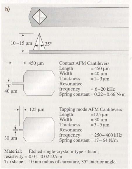
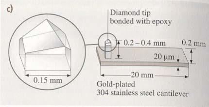
3 AFM Probe Construction Low spring constant (k to 10 2 N/m) Sharp protruding tip (r=5-50 nm) High resonance frequency 1 ω = 2 π k m Three common types of AFM tip normal supertip ultralever

4 Common types of cantilevers Si 3 N 4 Si Diamond
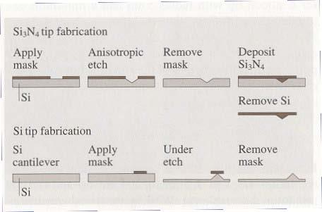
5 Fabrication of cantilevers


6 Calibration of cantilever Theoretical method Static method Dynamic method Measuring of thermal response of the cantilever Measuring of the change of resonance frequency caused by the addition of known masses E=300 GPa E=238 GPa ( Z ) ' Zt ks = Ztkc t
7 Superposition of two geometries

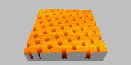
8 Reconvolution of the tip shape I II r d D=d real d D = D 2 4r

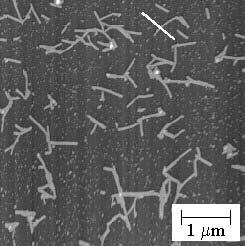
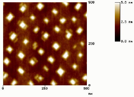
9 Deconvolution of the tip shape Tobacco Mosaic Virus (TMV) d~18 nm r-?
10 Calibration of the tip shape L 2r L h 2 L R = 4 r 2 L R = 2 h

 d = 2R (")
11 Useful formulas 2 d z = 8R d 2. 8nm z = d > 3nm d 2 ( 4d + 8R ) d = 2R ( ) z + z + h

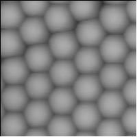
12 AFM Tip Artifacts We start off with an example of a good AFM image of 300 nm polystyrene spheres...

13 AFM Tip Artifacts Similar spheres imaged with a supposedly sharp tip
14 AFM Tip Artifacts This image should only contain images of large polysterene spheres

15 AFM Tip Artifacts Classical example of tip artifact, showing DNA and debris

16 AFM Tip Artifacts Here is a cute example of some serious artifacts. The obtained image looks like the three bears
17 Different types of forces relevant to AFM 4 3 F g = mg = πr ρg 3 3 ρ 1 g / cm r = 25 nm g = 9. 8 m / sec 2 9 F g 10 nn (a) A r F vdw = 2 6D 19 A = 10 J D = 0. 3 nm r = 25 nm F vdw ~ 5 nn F adh γ = 2 γ = 4πr γ ( γ γ ) 1/ 2 γ = 100 mj/m 2 s silica surface energy p s p = 25 mj/m 2 polymer surface energy F adh ~ 30 nn (d) Deformation forces (b) Capillary forces F cap = 4πRγ1 cos θ ~ 22nN F d = Ka R 3 ~ 6nN, a ~ 5 nm, the typical contact radius

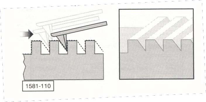
18 Blind Reconstruction AFM profile of a single bump What does this single scan line tell us about the topography of the tip and sample? The tip geometry can be no bigger than the obtained profile


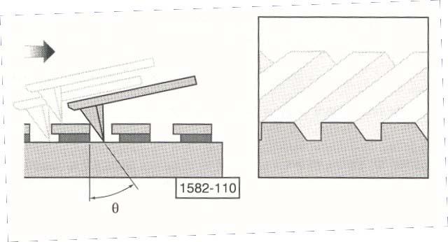
19 Blind Reconstruction Line scan having two bumps What does this tell us about the shape of the tip? Case 1: Tip with single apex

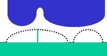
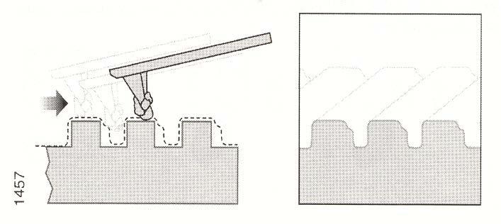
20 Case 2: double tip


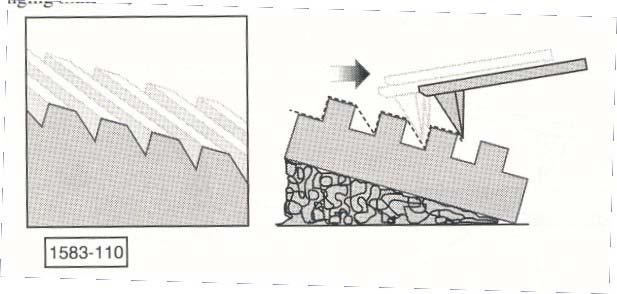
21 True three-dimensional scanning? One of the drawbacks of typical AFM is that the images obtained are not truely threedimentional. No matter how sharp the tip, the data collected can never access the underside of the sample. Petticoat effect-all images of objects having steep walls or undercut regions appear to have flared sides
22 Method for imaging sidewalls by AFM Martin, Wickramasinghe, Appl. Phys Lett 1994, 64, 2498 Can we get a similar image using a typical AFM and the boot-shaped tip? No!
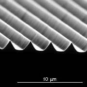
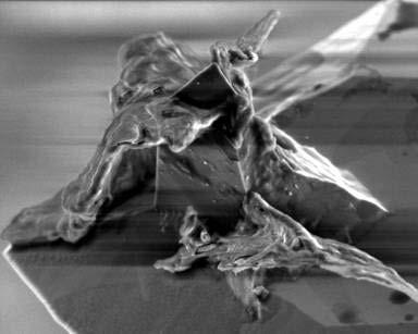
23 Titanium thin films 2 µm per 2 µm

24 The tip is not too bad, it just is not very sharp

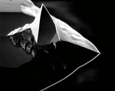
25 A subtle example of a double tip

26 Here is an image taken by a multiple tip

27 This is an image of a triple tip

28 Sometimes you just can t figure ou what is wrong with the tip- it just doesn t look right!

29 The tip broke or had a large contaminant dislodged while scanning down
30


31 TGT spikes delta-like function: 1 µm high, 1.5 µm apart


32 TGT spikes delta-like function: 1 µm high, 1.5 µm apart A formation of B2 bombers? The return of space invaders A school of fish, maybe? The eyes are rounded tips about 100nm in radius

33 Normal tip vs NT-tip


34 Conclusion: Golden rule of AFM spectroscopy: Every time one measures one obtains an image Not every time one obtains an artifact


35 Oxide-Sharpened Tips increasing aspect ratio reducing tip radius SiO 2 HF etching Aspect ration- 10:1 Radius r~1nm

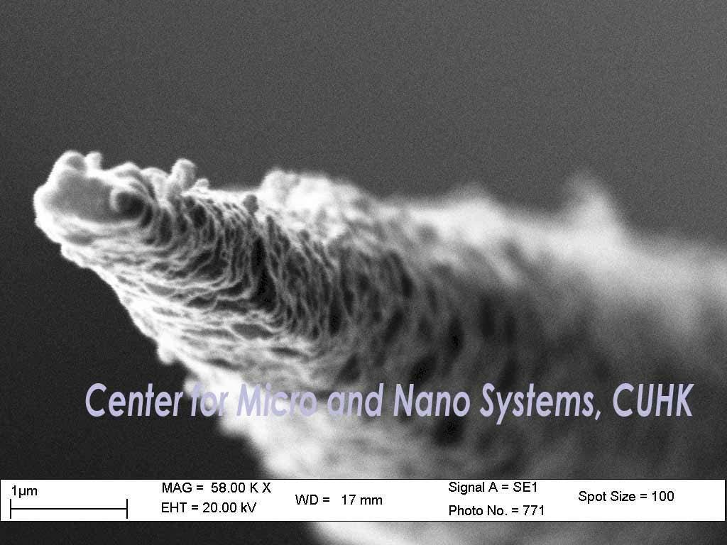
36 Electron beam deposition (EBD) High-aspect-ratio tips L=(1-5)µm R=(20-40)nm Carbon materials are deposed by the dissociation of background gases in the SEM vacuum chamber
nm Multiwalled carbon nanotubes (MWNT) (nested, concentrically arranged")
 Buckled nanotubes Labor intensive Not amenable to")
37 Carbon Nanotube Tips Single-walled carbon nanotubes (SWNT), d=(0.7-3)nm Multiwalled carbon nanotubes (MWNT) (nested, concentrically arranged SWNT, d=(3-50)nm High-aspect-ration AFM probes Very stiff, E=10 12 Pa (the stiffest known materials) Buckled nanotubes Labor intensive Not amenable to mass production


38 Pick-up Tips d=0.9nm d=2.8nm

 Presipitates carbon nucleates a")
39 Chemical Vapor deposition (CVD) Direct grow nanotubes onto AFM tip Heating of nanocatalyst particle (r~3.5 nm) Presipitates carbon nucleates a grow of nanotube

40 Direct grow of nanotubes Alumina/iron/molybdenumpowdered catalyst 2 nm in diameter 2µm in length Labor intensive Not amenable to mass production
41 Modes of operation
42 The common AFM modes contact mode tapping mode Contact mode Non-contact mode Intermittent mode
 The force on the tip is repulsive ~ a few nn The")

43 Contact mode AFM A tip is scanned across the sample while a feedback loop maintains a constant cantilever deflection (and force) The force on the tip is repulsive ~ a few nn The tip senses lateral and normal forces The tip contacts the surface through the adsorbed fluid layer Forces range from nano to micro N in ambient conditions and even lover (0.1 nn or less) in liquid

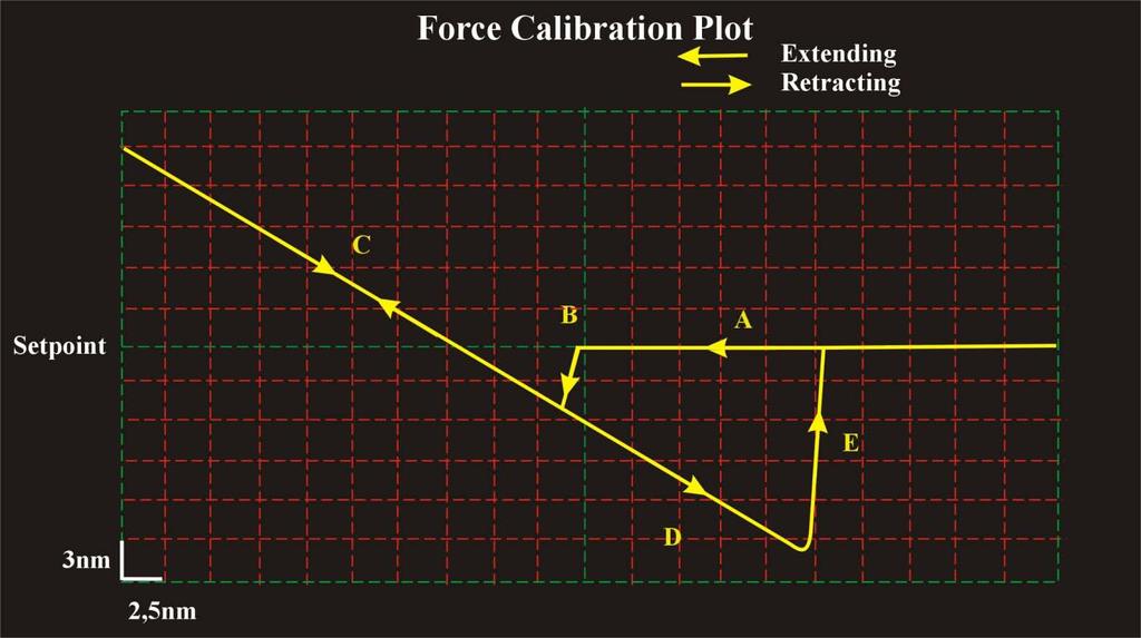
44 Force curve
45 Contact mode C Force D B Static mode Dynamic mode Oscillation amplitude Probe-sample distance, z A F > k, z at "B"is F = kz, k = z = 0. 1nm F ~ 1pN 0. 1 N / m, jump into a contact to "C"

46 Problems of the contact mode Large deformation forces ~ 100 nn Capillary forces F cap = 4πRγ1 cos θ ~ 22nN To solve the problem operation in liquid Elimination of capillary forces Reduction of van der Waals forces

47 Problems of the contact mode Large lateral (shear) forces ~ 100 nn To solve the problem non-contact mode


48 Non-contact Mode AFM Highly unstable mode Ultra high vacuum at low temperature
49 Tapping mode AFM A cantilever with attached tip is oscillated at its resonant frequency and scanned across the sample surface A constant oscillation amplitude (and thus a constant tip-sample interaction) are maintained during scanning. Typical amplitudes are nm Forces can be 200 pn or less The amplitue of the oscillations changes when the tip scans over bumps or depressions on a surface

50 Tapping mode AFM ω A kHz nm
51 Tapping mode AFM Force Static mode Dynamic mode Probe-sample distance, z A B C D Oscillation amplitude
52 Tapping mode AFM Three regimes of tapping mode: (i) Light tapping 0. 7 r 1 sp r sp = A sp A 0 (ii) Moderate tapping 0. 3 rsp 0. 7 (iii) Hard tapping rsp 0. 3

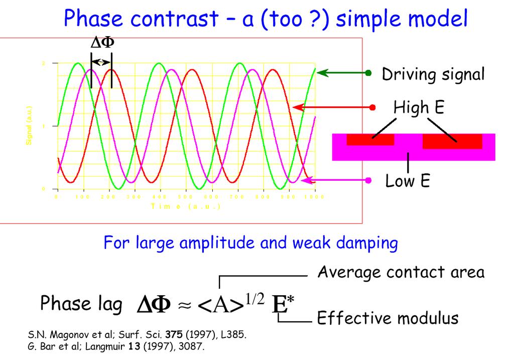
53 Tapping mode AFM Phase Imaging Driven force Actual responce Different characteristics of the sample different offset the phase
54
55
56
57

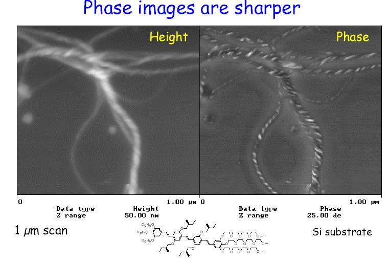
58 Examples of Phase Images AFM


59 Examples of Phase Images AFM


60 Examples of Phase Images AFM


61 Examples of Phase Images AFM

62 Examples of Phase Images AFM


63 Examples of Phase Images AFM

64 Examples of Phase Images AFM


65 Examples of Phase Images AFM


66 Examples of Phase Images AFM

67 Examples of Phase Images AFM

68 Examples of Phase Images AFM
69 Advantages and Disadvantages Contact Mode Advantages Disadvantages high scan speeds the only mode that can obtain atomic resolution images rough samples with extreme changes in topography can sometimes be scanned more easily lateral (shear) forces can distort features in the images the forces normal to the tip-sample interction can be high in air due to capillary forces from the adsorbed fluid layer on the sample surface the combination of lateral forces and high normal forces can result in reduced spatials resolution and may damage soft samples (i.e. biological samples, polymers) due to scraping
70 Advantages and Disadvantages Tapping mode Advantages higher lateral resolution on most samples (1 to 5 nm) lower forces and less damage to soft samples imaged in air lateral forces are virtually eliminated so there is no scraping Disadvantages slightly lower scan speed than contact mode AFM

71 Cantilevers used in contact and tapping modes k N / m k ~ 50 N / m

72 Contact vs Tapping modes

73 How to interpret height and phase TM-AFM images of a sample in terms of its physical and morphological properties?
General concept and defining characteristics of AFM. Dina Kudasheva Advisor: Prof. Mary K. Cowman
 General concept and defining characteristics of AFM Dina Kudasheva Advisor: Prof. Mary K. Cowman Overview Introduction History of the SPM invention Technical Capabilities Principles of operation Examples
Basic Laboratory. Materials Science and Engineering. Atomic Force Microscopy (AFM)
") Basic Laboratory Materials Science and Engineering Atomic Force Microscopy (AFM) M108 Stand: 20.10.2015 Aim: Presentation of an application of the AFM for studying surface morphology. Inhalt 1.Introduction...
Basic Laboratory Materials Science and Engineering Atomic Force Microscopy (AFM) M108 Stand: 20.10.2015 Aim: Presentation of an application of the AFM for studying surface morphology. Inhalt 1.Introduction...
Digital Instruments (DI) Multymode Nanoscope IIIa
 Multymode Nanoscope IIIa") Lecture 6 From Microsystems to the Nanoworld Freiburger Materialforschungszentrum Institut für Mikrosystemtechnik Basics of AFM AFM provides very hogh resolution images of various sample properties PSD
Lecture 6 From Microsystems to the Nanoworld Freiburger Materialforschungszentrum Institut für Mikrosystemtechnik Basics of AFM AFM provides very hogh resolution images of various sample properties PSD
Scanning Force Microscopy
 Scanning Force Microscopy Roland Bennewitz Rutherford Physics Building 405 Phone 398-3058 roland.bennewitz@mcgill.ca Scanning Probe is moved along scan lines over a sample surface 1 Force Microscopy Data
Instrumentation and Operation
 Instrumentation and Operation 1 STM Instrumentation COMPONENTS sharp metal tip scanning system and control electronics feedback electronics (keeps tunneling current constant) image processing system data
Atomic Force Microscopy imaging and beyond
 Atomic Force Microscopy imaging and beyond Arif Mumtaz Magnetism and Magnetic Materials Group Department of Physics, QAU Coworkers: Prof. Dr. S.K.Hasanain M. Tariq Khan Alam Imaging and beyond Scanning
Contents. What is AFM? History Basic principles and devices Operating modes Application areas Advantages and disadvantages
 Contents What is AFM? History Basic principles and devices Operating modes Application areas Advantages and disadvantages Figure1: 2004 Seth Copen Goldstein What is AFM? A type of Scanning Probe Microscopy
Lecture 12: Biomaterials Characterization in Aqueous Environments
 3.051J/20.340J 1 Lecture 12: Biomaterials Characterization in Aqueous Environments High vacuum techniques are important tools for characterizing surface composition, but do not yield information on surface
Lecture 4 Scanning Probe Microscopy (SPM)
") Lecture 4 Scanning Probe Microscopy (SPM) General components of SPM; Tip --- the probe; Cantilever --- the indicator of the tip; Tip-sample interaction --- the feedback system; Scanner --- piezoelectric
Lecture 4 Scanning Probe Microscopy (SPM) General components of SPM; Tip --- the probe; Cantilever --- the indicator of the tip; Tip-sample interaction --- the feedback system; Scanner --- piezoelectric
Techniken der Oberflächenphysik (Techniques of Surface Physics)
") Techniken der Oberflächenphysik (Techniques of Surface Physics) Prof. Yong Lei & Dr. Yang Xu Fachgebiet 3D-Nanostrukturierung, Institut für Physik Contact: yong.lei@tu-ilmenau.de yang.xu@tu-ilmenau.de
Techniken der Oberflächenphysik (Techniques of Surface Physics) Prof. Yong Lei & Dr. Yang Xu Fachgebiet 3D-Nanostrukturierung, Institut für Physik Contact: yong.lei@tu-ilmenau.de yang.xu@tu-ilmenau.de
Point mass approximation. Rigid beam mechanics. spring constant k N effective mass m e. Simple Harmonic Motion.. m e z = - k N z
 Free end Rigid beam mechanics Fixed end think of cantilever as a mass on a spring Point mass approximation z F Hooke s law k N = F / z This is beam mechanics, standard in engineering textbooks. For a rectangular
AFM for Measuring Surface Topography and Forces
 ENB 2007 07.03.2007 AFM for Measuring Surface Topography and Forces Andreas Fery Scanning Probe : What is it and why do we need it? AFM as a versatile tool for local analysis and manipulation Dates Course
Scanning Probe Microscopy. Amanda MacMillan, Emmy Gebremichael, & John Shamblin Chem 243: Instrumental Analysis Dr. Robert Corn March 10, 2010
 Scanning Probe Microscopy Amanda MacMillan, Emmy Gebremichael, & John Shamblin Chem 243: Instrumental Analysis Dr. Robert Corn March 10, 2010 Scanning Probe Microscopy High-Resolution Surface Analysis
NIS: what can it be used for?
 AFM @ NIS: what can it be used for? Chiara Manfredotti 011 670 8382/8388/7879 chiara.manfredotti@to.infn.it Skype: khiaram 1 AFM: block scheme In an Atomic Force Microscope (AFM) a micrometric tip attached
STM: Scanning Tunneling Microscope
 STM: Scanning Tunneling Microscope Basic idea STM working principle Schematic representation of the sample-tip tunnel barrier Assume tip and sample described by two infinite plate electrodes Φ t +Φ s =
Module 26: Atomic Force Microscopy. Lecture 40: Atomic Force Microscopy 3: Additional Modes of AFM
 Module 26: Atomic Force Microscopy Lecture 40: Atomic Force Microscopy 3: Additional Modes of AFM 1 The AFM apart from generating the information about the topography of the sample features can be used
Scanning Force Microscopy II
 Scanning Force Microscopy II Measurement modes Magnetic force microscopy Artifacts Lars Johansson 1 SFM - Forces Chemical forces (short range) Van der Waals forces Electrostatic forces (long range) Capillary
Imaging Methods: Scanning Force Microscopy (SFM / AFM)
") Imaging Methods: Scanning Force Microscopy (SFM / AFM) The atomic force microscope (AFM) probes the surface of a sample with a sharp tip, a couple of microns long and often less than 100 Å in diameter.
Imaging Methods: Scanning Force Microscopy (SFM / AFM) The atomic force microscope (AFM) probes the surface of a sample with a sharp tip, a couple of microns long and often less than 100 Å in diameter.
Program Operacyjny Kapitał Ludzki SCANNING PROBE TECHNIQUES - INTRODUCTION
 Program Operacyjny Kapitał Ludzki SCANNING PROBE TECHNIQUES - INTRODUCTION Peter Liljeroth Department of Applied Physics, Aalto University School of Science peter.liljeroth@aalto.fi Projekt współfinansowany
Characterization of MEMS Devices
 MEMS: Characterization Characterization of MEMS Devices Prasanna S. Gandhi Assistant Professor, Department of Mechanical Engineering, Indian Institute of Technology, Bombay, Recap Characterization of MEMS
Supporting Information
 Supporting Information Analysis Method for Quantifying the Morphology of Nanotube Networks Dusan Vobornik*, Shan Zou and Gregory P. Lopinski Measurement Science and Standards, National Research Council
Scanning Tunneling Microscopy
 Scanning Tunneling Microscopy Scanning Direction References: Classical Tunneling Quantum Mechanics Tunneling current Tunneling current I t I t (V/d)exp(-Aφ 1/2 d) A = 1.025 (ev) -1/2 Å -1 I t = 10 pa~10na
SUPPLEMENTARY NOTES Supplementary Note 1: Fabrication of Scanning Thermal Microscopy Probes
 SUPPLEMENTARY NOTES Supplementary Note 1: Fabrication of Scanning Thermal Microscopy Probes Fabrication of the scanning thermal microscopy (SThM) probes is summarized in Supplementary Fig. 1 and proceeds
AFM Imaging In Liquids. W. Travis Johnson PhD Agilent Technologies Nanomeasurements Division
 AFM Imaging In Liquids W. Travis Johnson PhD Agilent Technologies Nanomeasurements Division Imaging Techniques: Scales Proteins 10 nm Bacteria 1μm Red Blood Cell 5μm Human Hair 75μm Si Atom Spacing 0.4nm
Vibration Studying of AFM Piezoelectric Microcantilever Subjected to Tip-Nanoparticle Interaction
 Journal of Novel Applied Sciences Available online at www.jnasci.org 2013 JNAS Journal-2013-2-S/806-811 ISSN 2322-5149 2013 JNAS Vibration Studying of AFM Piezoelectric Microcantilever Subjected to Tip-Nanoparticle
Università degli Studi di Bari "Aldo Moro"
 Università degli Studi di Bari "Aldo Moro" Table of contents 1. Introduction to Atomic Force Microscopy; 2. Introduction to Raman Spectroscopy; 3. The need for a hybrid technique Raman AFM microscopy;
Scanning Probe Microscopy (SPM)
") Scanning Probe Microscopy (SPM) Scanning Tunneling Microscopy (STM) --- G. Binnig, H. Rohrer et al, (1982) Near-Field Scanning Optical Microscopy (NSOM) --- D. W. Pohl (1982) Atomic Force Microscopy (AFM)
Scanning Probe Microscopy (SPM) Scanning Tunneling Microscopy (STM) --- G. Binnig, H. Rohrer et al, (1982) Near-Field Scanning Optical Microscopy (NSOM) --- D. W. Pohl (1982) Atomic Force Microscopy (AFM)
Scanning Tunneling Microscopy
 Scanning Tunneling Microscopy References: 1. G. Binnig, H. Rohrer, C. Gerber, and Weibel, Phys. Rev. Lett. 49, 57 (1982); and ibid 50, 120 (1983). 2. J. Chen, Introduction to Scanning Tunneling Microscopy,
SOLID STATE PHYSICS PHY F341. Dr. Manjuladevi.V Associate Professor Department of Physics BITS Pilani
 SOLID STATE PHYSICS PHY F341 Dr. Manjuladevi.V Associate Professor Department of Physics BITS Pilani 333031 manjula@bits-pilani.ac.in Characterization techniques SEM AFM STM BAM Outline What can we use
Chapter 12. Nanometrology. Oxford University Press All rights reserved.
 Chapter 12 Nanometrology Introduction Nanometrology is the science of measurement at the nanoscale level. Figure illustrates where nanoscale stands in relation to a meter and sub divisions of meter. Nanometrology
Intermittent-Contact Mode Force Microscopy & Electrostatic Force Microscopy (EFM)
") WORKSHOP Nanoscience on the Tip Intermittent-Contact Mode Force Microscopy & Electrostatic Force Microscopy (EFM) Table of Contents: 1. Motivation... 1. Simple Harmonic Motion... 1 3. AC-Mode Imaging...
WORKSHOP Nanoscience on the Tip Intermittent-Contact Mode Force Microscopy & Electrostatic Force Microscopy (EFM) Table of Contents: 1. Motivation... 1. Simple Harmonic Motion... 1 3. AC-Mode Imaging...
Atomic Force Microscopy (AFM) Part I
 Part I") Atomic Force Microscopy (AFM) Part I CHEM-L2000 Eero Kontturi 6 th March 2018 Lectures on AFM Part I Principles and practice Imaging of native materials, including nanocellulose Part II Surface force measurements
Atomic Force Microscopy (AFM) Part I CHEM-L2000 Eero Kontturi 6 th March 2018 Lectures on AFM Part I Principles and practice Imaging of native materials, including nanocellulose Part II Surface force measurements
INTRODUCTION TO SCA\ \I\G TUNNELING MICROSCOPY
 INTRODUCTION TO SCA\ \I\G TUNNELING MICROSCOPY SECOND EDITION C. JULIAN CHEN Department of Applied Physics and Applied Mathematics, Columbia University, New York OXFORD UNIVERSITY PRESS Contents Preface
Nanostructure. Materials Growth Characterization Fabrication. More see Waser, chapter 2
 Nanostructure Materials Growth Characterization Fabrication More see Waser, chapter 2 Materials growth - deposition deposition gas solid Physical Vapor Deposition Chemical Vapor Deposition Physical Vapor
And Manipulation by Scanning Probe Microscope
 Basic 15 Nanometer Scale Measurement And Manipulation by Scanning Probe Microscope Prof. K. Fukuzawa Dept. of Micro/Nano Systems Engineering Nagoya University I. Basics of scanning probe microscope Basic
Scanning Probe Microscopy (SPM)
") CHEM53200: Lecture 9 Scanning Probe Microscopy (SPM) Major reference: 1. Scanning Probe Microscopy and Spectroscopy Edited by D. Bonnell (2001). 2. A practical guide to scanning probe microscopy by Park
CHEM53200: Lecture 9 Scanning Probe Microscopy (SPM) Major reference: 1. Scanning Probe Microscopy and Spectroscopy Edited by D. Bonnell (2001). 2. A practical guide to scanning probe microscopy by Park
Keysight Technologies Carbon Nanotube Tips for MAC Mode AFM Measurements in Liquids. Application Note
 Keysight Technologies Carbon Nanotube Tips for MAC Mode AFM Measurements in Liquids Application Note Introduction Atomic force microscopy (AFM) is a powerful technique in revealing the microscopic structure
Introduction to Nanomechanics: Magnetic resonance imaging with nanomechanics
 Introduction to Nanomechanics: Magnetic resonance imaging with nanomechanics Martino Poggio Swiss Nanoscience Institute Department of Physics University of Basel Switzerland Nano I, Herbstsemester 2009
Measurement of hardness, surface potential, and charge distribution with dynamic contact mode electrostatic force microscope
 REVIEW OF SCIENTIFIC INSTRUMENTS VOLUME 70, NUMBER 3 MARCH 1999 Measurement of hardness, surface potential, and charge distribution with dynamic contact mode electrostatic force microscope J. W. Hong,
VEDA - Virtual Environment for Dynamic Atomic Force Microscopy
 VEDA - Virtual Environment for Dynamic Atomic Force Microscopy John Melcher, Daniel Kiracofe, doctoral students Steven Johnson, undergraduate Shuiqing Hu, Veeco Arvind Raman, Associate Professor Mechanical
3.052 Nanomechanics of Materials and Biomaterials Thursday 02/08/06 Prof. C. Ortiz, MIT-DMSE I LECTURE 2 : THE FORCE TRANSDUCER
 I LECTURE 2 : THE FORCE TRANSDUCER Outline : LAST TIME : WHAT IS NANOMECHANICS... 2 HOW CAN WE MEASURE SUCH TINY FORCES?... 3 EXAMPLE OF A FORCE TRANSDUCER... 4 Microfabricated cantilever beams with nanosized
SCANNING-PROBE TECHNIQUES OR APPARATUS; APPLICATIONS OF SCANNING-PROBE TECHNIQUES, e.g. SCANNING PROBE MICROSCOPY [SPM]
![SCANNING-PROBE TECHNIQUES OR APPARATUS; APPLICATIONS OF SCANNING-PROBE TECHNIQUES, e.g. SCANNING PROBE MICROSCOPY [SPM]](/thumbs/81/83165631.jpg "SCANNING-PROBE TECHNIQUES OR APPARATUS; APPLICATIONS OF SCANNING-PROBE TECHNIQUES, e.g. SCANNING PROBE MICROSCOPY [SPM]") G01Q SCANNING-PROBE TECHNIQUES OR APPARATUS; APPLICATIONS OF SCANNING-PROBE TECHNIQUES, e.g. SCANNING PROBE MICROSCOPY [SPM] Scanning probes, i.e. devices having at least a tip of nanometre sized dimensions
G01Q SCANNING-PROBE TECHNIQUES OR APPARATUS; APPLICATIONS OF SCANNING-PROBE TECHNIQUES, e.g. SCANNING PROBE MICROSCOPY [SPM] Scanning probes, i.e. devices having at least a tip of nanometre sized dimensions
Magnetic Force Microscopy practical
 European School on Magnetism 2015 From basic magnetic concepts to spin currents Magnetic Force Microscopy practical Organized by: Yann Perrin, Michal Staňo and Olivier Fruchart Institut NEEL (CNRS & Univ.
Introduction to Scanning Tunneling Microscopy
 Introduction to Scanning Tunneling Microscopy C. JULIAN CHEN IBM Research Division Thomas J. Watson Research Center Yorktown Heights, New York New York Oxford OXFORD UNIVERSITY PRESS 1993 CONTENTS List
Scanning Probe Microscopy
 1 Scanning Probe Microscopy Dr. Benjamin Dwir Laboratory of Physics of Nanostructures (LPN) Benjamin.dwir@epfl.ch PH.D3.344 Outline: Introduction: What is SPM, history STM AFM Image treatment Advanced
Introduction to Scanning Probe Microscopy Zhe Fei
 Introduction to Scanning Probe Microscopy Zhe Fei Phys 590B, Apr. 2019 1 Outline Part 1 SPM Overview Part 2 Scanning tunneling microscopy Part 3 Atomic force microscopy Part 4 Electric & Magnetic force
Atomic and molecular interactions. Scanning probe microscopy.
 Atomic and molecular interactions. Scanning probe microscopy. Balázs Kiss Nanobiotechnology and Single Molecule Research Group, Department of Biophysics and Radiation Biology 27. November 2013. 2 Atomic
CNPEM Laboratório de Ciência de Superfícies
 Investigating electrical charged samples by scanning probe microscopy: the influence to magnetic force microscopy and atomic force microscopy phase images. Carlos A. R. Costa, 1 Evandro M. Lanzoni, 1 Maria
The Powerful Diversity of the AFM Probe
 The Powerful Diversity of the AFM Probe Stefan B. Kaemmer, Bruker Nano Surfaces Division, Santa Barbara, CA 93117 stefan.kaemmer@bruker-nano.com March 21, 2011 Introduction The tip allows us to measure
Scanning Probe Microscopy. EMSE-515 F. Ernst
 Scanning Probe Microscopy EMSE-515 F. Ernst 1 Literature 2 3 Scanning Probe Microscopy: The Lab on a Tip by Ernst Meyer,Ans Josef Hug,Roland Bennewitz 4 Scanning Probe Microscopy and Spectroscopy : Theory,
Metal-coated carbon nanotube tips for Magnetic Force Microscopy
 Metal-coated carbon nanotube tips for Magnetic Force Microscopy Zhifeng Deng 1,4, Erhan Yenilmez 2,4, Josh Leu 1,4, J.E. Hoffman 2,4, Eric Straver 2,4, Hongjie Dai 3,4, Kathryn A. Moler 1,2,4 1 Department
Chapter 10. Nanometrology. Oxford University Press All rights reserved.
 Chapter 10 Nanometrology Oxford University Press 2013. All rights reserved. 1 Introduction Nanometrology is the science of measurement at the nanoscale level. Figure illustrates where nanoscale stands
Scanning Probe Microscopy. L. J. Heyderman
 1 Scanning Probe Microscopy 2 Scanning Probe Microscopy If an atom was as large as a ping-pong ball......the tip would have the size of the Matterhorn! 3 Magnetic Force Microscopy Stray field interaction
Nitride HFETs applications: Conductance DLTS
 Nitride HFETs applications: Conductance DLTS The capacitance DLTS cannot be used for device trap profiling as the capacitance for the gate will be very small Conductance DLTS is similar to capacitance
PHY 481/581. Some classical/quantum physics for the nanometer length scale.
 PHY 481/581 Some classical/quantum physics for the nanometer length scale http://creativecommons.org/licenses/by-nc-sa/3.0/ 1 What is nano-science? the science of materials whose properties scale with
Measurements of interaction forces in (biological) model systems
 model systems") Measurements of interaction forces in (biological) model systems Marina Ruths Department of Chemistry, UMass Lowell What can force measurements tell us about a system? Depending on the technique, we might
Measurements of interaction forces in (biological) model systems Marina Ruths Department of Chemistry, UMass Lowell What can force measurements tell us about a system? Depending on the technique, we might
SUPPLEMENTARY INFORMATION
 1. Supplementary Methods Characterization of AFM resolution We employed amplitude-modulation AFM in non-contact mode to characterize the topography of the graphene samples. The measurements were performed
Lecture Note October 1, 2009 Nanostructure characterization techniques
 Lecture Note October 1, 29 Nanostructure characterization techniques UT-Austin PHYS 392 T, unique # 5977 ME 397 unique # 1979 CHE 384, unique # 151 Instructor: Professor C.K. Shih Subjects: Applications
Introduction to Scanning Probe Microscopy
 WORKSHOP Nanoscience on the Tip Introduction to Scanning Probe Microscopy Table of Contents: 1 Historic Perspectives... 1 2 Scanning Force Microscopy (SFM)... 2 2.1. Contact Mode... 2 2.2. AC Mode Imaging...
Improving the accuracy of Atomic Force Microscope based nanomechanical measurements. Bede Pittenger Bruker Nano Surfaces, Santa Barbara, CA, USA
 Improving the accuracy of Atomic Force Microscope based nanomechanical measurements Bede Pittenger Bruker Nano Surfaces, Santa Barbara, CA, USA How can we improve accuracy in our nanomechanical measurements?
Review. Surfaces of Biomaterials. Characterization. Surface sensitivity
 Surfaces of Biomaterials Three lectures: 1.23.05 Surface Properties of Biomaterials 1.25.05 Surface Characterization 1.27.05 Surface and Protein Interactions Review Bulk Materials are described by: Chemical
Kavli Workshop for Journalists. June 13th, CNF Cleanroom Activities
 Kavli Workshop for Journalists June 13th, 2007 CNF Cleanroom Activities Seeing nm-sized Objects with an SEM Lab experience: Scanning Electron Microscopy Equipment: Zeiss Supra 55VP Scanning electron microscopes
Scanning Probe Microscopies (SPM)
") Scanning Probe Microscopies (SPM) Nanoscale resolution af objects at solid surfaces can be reached with scanning probe microscopes. They allow to record an image of the surface atomic arrangement in direct
Scanning Probe Microscopies (SPM) Nanoscale resolution af objects at solid surfaces can be reached with scanning probe microscopes. They allow to record an image of the surface atomic arrangement in direct
Dopant Concentration Measurements by Scanning Force Microscopy
 73.40L Scanning Microsc. Microanal. Microstruct. 551 Classification Physics Abstracts - - 61.16P 73.00 Dopant Concentration Measurements by Scanning Force Microscopy via p-n Junctions Stray Fields Jacopo
Features of static and dynamic friction profiles in one and two dimensions on polymer and atomically flat surfaces using atomic force microscopy
 Features of static and dynamic friction profiles in one and two dimensions on polymer and atomically flat surfaces using atomic force microscopy Author Watson, Gregory, Watson, Jolanta Published 008 Journal
Chapter 5 Nanomanipulation. Chapter 5 Nanomanipulation. 5.1: With a nanotube. Cutting a nanotube. Moving a nanotube
 Objective: learn about nano-manipulation techniques with a STM or an AFM. 5.1: With a nanotube Moving a nanotube Cutting a nanotube Images at large distance At small distance : push the NT Voltage pulse
Crystalline Surfaces for Laser Metrology
 Crystalline Surfaces for Laser Metrology A.V. Latyshev, Institute of Semiconductor Physics SB RAS, Novosibirsk, Russia Abstract: The number of methodological recommendations has been pronounced to describe
Initial Stages of Growth of Organic Semiconductors on Graphene
 Initial Stages of Growth of Organic Semiconductors on Graphene Presented by: Manisha Chhikara Supervisor: Prof. Dr. Gvido Bratina University of Nova Gorica Outline Introduction to Graphene Fabrication
BDS2016 Tutorials: Local Dielectric Spectroscopy by Scanning Probes
 BDS2016 Tutorials: Local Dielectric Spectroscopy by Scanning Probes Massimiliano Labardi CNR Institute for Physico-Chemical Processes (IPCF) Pisa (Italy) OUTLINE Broadband Dielectric Spectroscopy (BDS):
3.052 Nanomechanics of Materials and Biomaterials Thursday 02/22/07 Prof. C. Ortiz, MIT-DMSE
 I LECTURE 5: AFM IMAGING Outline : LAST TIME : HRFS AND FORCE-DISTANCE CURVES... 2 ATOMIC FORCE MICROSCOPY : GENERAL COMPONENTS AND FUNCTIONS... 3 Deflection vs. Height Images... 4 3D Plots and 2D Section
Contents. Principles: Theory and Practice
 Contents Part I Principles: Theory and Practice 1 Physical Principles of Scanning Probe Microscopy Imaging... 3 1.1 Introduction... 3 1.2 The Physical Principles of Atomic Force Microscopy... 4 1.2.1 Forces
SUPPLEMENTARY INFORMATION
 SUPPLMNTARY INFORMATION Hindered rolling and friction anisotropy in supported carbon nanotubes Marcel Lucas 1, Xiaohua Zhang +, Ismael Palaci 1, Christian Klinke 3, rio Tosatti, 4 * and lisa Riedo 1 *
Instability & Pattering of Thin Polymer Films Prof. R. Mukherjee Department of Chemical Engineering Indian Institute of Technology Kharagpur
 Instability & Pattering of Thin Polymer Films Prof. R. Mukherjee Department of Chemical Engineering Indian Institute of Technology Kharagpur Lecture No#26 Atomic Force Microscope V (Refer Slide Time: 00:34)
Frictional characteristics of exfoliated and epitaxial graphene
 Frictional characteristics of exfoliated and epitaxial graphene Young Jun Shin a,b, Ryan Stromberg c, Rick Nay c, Han Huang d, Andrew T. S. Wee d, Hyunsoo Yang a,b,*, Charanjit S. Bhatia a a Department
MAGNETIC FORCE MICROSCOPY
 University of Ljubljana Faculty of Mathematics and Physics Department of Physics SEMINAR MAGNETIC FORCE MICROSCOPY Author: Blaž Zupančič Supervisor: dr. Igor Muševič February 2003 Contents 1 Abstract 3
Scanning Force Microscopy And Related Techniques. With the help of.
 With the help of. 1. Yosi Shacham TAU 2. Yossi Rosenwacks TAU 3. Julio Gomez-Herrero UAM 4. Adriana Gil - UAM 5. Serge Lemay - Delft 6. Hezy Cohen - HUJI 7. Scanning Force Microscopy And Related Techniques
Integrating MEMS Electro-Static Driven Micro-Probe and Laser Doppler Vibrometer for Non-Contact Vibration Mode SPM System Design
 Tamkang Journal of Science and Engineering, Vol. 12, No. 4, pp. 399 407 (2009) 399 Integrating MEMS Electro-Static Driven Micro-Probe and Laser Doppler Vibrometer for Non-Contact Vibration Mode SPM System
Lorentz Contact Resonance for viscoelastic measurements of polymer blends
 The world leader in nanoscale IR spectroscopy for viscoelastic measurements of polymer blends (LCR) reliably compares viscoleastic properties with nanoscale spatial resolution With no moving parts in the
MSN551 LITHOGRAPHY II
 MSN551 Introduction to Micro and Nano Fabrication LITHOGRAPHY II E-Beam, Focused Ion Beam and Soft Lithography Why need electron beam lithography? Smaller features are required By electronics industry:
Magnetic Resonance Force Microscopy. Christian Degen Department of Physics, ETH Zurich, Switzerland
 Magnetic Resonance Force Microscopy Christian Degen Department of Physics, ETH Zurich, Switzerland CIMST Summer School 2014 From Andreas Trabesinger / Wikipedia Scale of things 1m 1mm 1µm 1-100 nm 1nm
Nova 600 NanoLab Dual beam Focused Ion Beam IITKanpur
 Nova 600 NanoLab Dual beam Focused Ion Beam system @ IITKanpur Dual Beam Nova 600 Nano Lab From FEI company (Dual Beam = SEM + FIB) SEM: The Electron Beam for SEM Field Emission Electron Gun Energy : 500
Lecture 26 MNS 102: Techniques for Materials and Nano Sciences
 Lecture 26 MNS 102: Techniques for Materials and Nano Sciences Reference: #1 C. R. Brundle, C. A. Evans, S. Wilson, "Encyclopedia of Materials Characterization", Butterworth-Heinemann, Toronto (1992),
AFM: Atomic Force Microscopy II
 AM: Atomic orce Microscopy II Jan Knudsen The MAX IV laboratory & Division of synchrotron radiation research K522-523 (Sljus) 4 th of May, 2018 http://www.sljus.lu.se/staff/rainer/spm.htm Last time: The
MS482 Materials Characterization ( 재료분석 ) Lecture Note 11: Scanning Probe Microscopy. Byungha Shin Dept. of MSE, KAIST
 Lecture Note 11: Scanning Probe Microscopy. Byungha Shin Dept. of MSE, KAIST") 2015 Fall Semester MS482 Materials Characterization ( 재료분석 ) Lecture Note 11: Scanning Probe Microscopy Byungha Shin Dept. of MSE, KAIST 1 Course Information Syllabus 1. Overview of various characterization
2015 Fall Semester MS482 Materials Characterization ( 재료분석 ) Lecture Note 11: Scanning Probe Microscopy Byungha Shin Dept. of MSE, KAIST 1 Course Information Syllabus 1. Overview of various characterization
EE C247B / ME C218 INTRODUCTION TO MEMS DESIGN SPRING 2016 C. NGUYEN PROBLEM SET #4
 Issued: Wednesday, March 4, 2016 PROBLEM SET #4 Due: Monday, March 14, 2016, 8:00 a.m. in the EE C247B homework box near 125 Cory. 1. This problem considers bending of a simple cantilever and several methods
RHK Technology Brief
 The Atomic Force Microscope as a Critical Tool for Research in Nanotribology Rachel Cannara and Robert W. Carpick Nanomechanics Laboratory, University of Wisconsin Madison Department of Engineering Physics,
Ecole Franco-Roumaine : Magnétisme des systèmes nanoscopiques et structures hybrides - Brasov, Modern Analytical Microscopic Tools
 1. Introduction Solid Surfaces Analysis Group, Institute of Physics, Chemnitz University of Technology, Germany 2. Limitations of Conventional Optical Microscopy 3. Electron Microscopies Transmission Electron
b imaging by a double tip potential
 Supplementary Figure Measurement of the sheet conductance. Resistance as a function of probe spacing including D and 3D fits. The distance is plotted on a logarithmic scale. The inset shows corresponding
(Scanning Probe Microscopy)
") (Scanning Probe Microscopy) Ing-Shouh Hwang (ishwang@phys.sinica.edu.tw) Institute of Physics, Academia Sinica, Taipei, Taiwan References 1. G. Binnig, H. Rohrer, C. Gerber, and Weibel, Phys. Rev. Lett.
(Scanning Probe Microscopy) Ing-Shouh Hwang (ishwang@phys.sinica.edu.tw) Institute of Physics, Academia Sinica, Taipei, Taiwan References 1. G. Binnig, H. Rohrer, C. Gerber, and Weibel, Phys. Rev. Lett.
Magnetic ordering in two-dimensional. nanoparticle assemblies
 Magnetic ordering in two-dimensional nanoparticle assemblies Pedro Zeijlmans van Emmichoven Faculty of Science, Utrecht University Leiden, June 18 th, 2007 Collaborators Mirela Georgescu Mark Klokkenburg
Effect of AFM Cantilever Geometry on the DPL Nanomachining process
 Int J Advanced Design and Manufacturing Technology, Vol. 9/ No. 4/ December 2016 75 Effect of AFM Cantilever Geometry on the DPL Nanomachining process A. R. Norouzi Department of New Sciences and Technologies,
Softlithography and Atomic Force Microscopy
 Praktikum I, Autumn Semester 2008/09 Experiment 13/14; 03.12.2008 Softlithography and Atomic Force Microscopy Authors: Claudio Zihlmann (zclaudio@student.ethz.ch) and Philippe Knüsel (pknuesel@student.ethz.ch)
3.052 Nanomechanics of Materials and Biomaterials Thursday 02/22/07 Prof. C. Ortiz, MIT-DMSE
 I LECTURE 5: AFM IMAGING Outline : LAST TIME : HRFS AND FORCE-DISTANCE CURVES... 2 ATOMIC FORCE MICROSCOPY : GENERAL COMPONENTS AND FUNCTIONS... 3 Deflection vs. Height Images... 4 3D Plots and 2D Section
Lorentz Contact Resonance for viscoelastic measurements of polymer blends
 The nanoscale spectroscopy company The world leader in nanoscale IR spectroscopy Lorentz Contact Resonance for viscoelastic measurements of polymer blends Lorentz Contact Resonance (LCR) reliably compares
Nanostructure Fabrication Using Selective Growth on Nanosize Patterns Drawn by a Scanning Probe Microscope
 Nanostructure Fabrication Using Selective Growth on Nanosize Patterns Drawn by a Scanning Probe Microscope Kentaro Sasaki, Keiji Ueno and Atsushi Koma Department of Chemistry, The University of Tokyo,
A CONTROL SYSTEMS PERSPECTIVE ON NANOINTERROGATION
 A CONTROL SYSTEMS PERSPECTIVE ON NANOINTERROGATION Scanning Probe Microscopy At the 1959 annual meeting of the American Physical Society, Richard Feynman gave a seminal talk titled There s Plenty of Room
Microscopie a stilo: principi ed esempi di applicazione
 Microscopie a stilo: principi ed esempi di applicazione Adele Sassella Dipartimento di Scienza dei Materiali Università degli Studi di Milano Bicocca adele.sassella@unimib.it Pavia, 22 aprile 2009 SCANNING
Scanning Force Microscopy And Related Techniques
 Scanning Force Microscopy And Related Techniques Danny Porath 2003 With the help of. 1. Yosi Shacham TAU 2. Yossi Rosenwacks TAU 3. Julio Gomez-Herrero UAM 4. Adriana Gil - UAM 5. Serge Lemay - Delft 6.
Application of electrostatic force microscopy in nanosystem diagnostics
 Materials Science, Vol., No. 3, 003 Application of electrostatic force microscopy in nanosystem diagnostics TEODOR P. GOTSZALK *, PIOTR GRABIEC, IVO W. RANGELOW 3 Fulty of Microsystem Electronics and Photonics,
Magnetic nanoparticles containing soft-hard diblock
 Electronic Supplementary Material (ESI) for Nanoscale. This journal is The Royal Society of Chemistry 2018 Electronic Supplementary Information Magnetic nanoparticles containing soft-hard diblock copolymer