Singular Nano-Photonics: hydrodynamics-inspired light trapping & routing Svetlana V. Boriskina
|
|
|
- Bruno Mathews
- 5 years ago
- Views:
Transcription
1 Singular Nano-Photonics: hydrodynamics-inspired light trapping & routing Svetlana V. Boriskina Department of Mechanical Engineering Massachusetts Institute of Technology

 Image")
2 2 Cat. F5 tornado (Manitoba, Canada, June 2007) Image credit: Juri Hahhal


3 Ray picture dominates conventional thinking about light propagation 3 A. Mavrokefalos et al, Nano Lett. 12, , 2012 Image credit: Teresa Matfield


4 Plasmonic design makes use of antenna theory Dipole antenna analog: Hertz dipole antenna analog: 50nm Dipole moment induced on nanoparticle generates secondary radiation field

5 Plasmonic design makes use of antenna theory Phased antenna array analogs: Dipole moments induced on each nanoparticle constructively interfere through far-field radiation


6 Light trapping schemes typically rely on constructive interference of light rays 6 scattering field enhancement waveguiding J. VanCleave, Colors & Thin-Film Interference, John Wiley & Sons, Inc. Atwater & Polman, Nature Mater. 2010
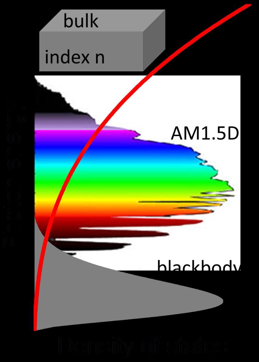
7 There is another way: making use of destructive interference 7 zero intensity = indefinite phase E ( r, t ) U ( r ) exp i ( ( r ) t ) phase vortex Black holes are where God divided by zero Steven Alexander Wright
 t ) Credit: istockphoto.")
8 There is another way: making use of destructive interference 8 zero intensity = indefinite phase E ( r, t ) U ( r ) exp i ( ( r ) t ) Credit: istockphoto.com/david Ciemny Black holes are where God divided by zero Steven Alexander Wright


9 There is another way: making use of destructive interference 9 Optical energy flows in the direction of the phase change phase vortex flow vortex Black holes are where God divided by zero Steven Alexander Wright
 Springer, 2013")
10 Hydrodynamic analogy of light trapping 10 Image credit: Teresa Matfield Image credit: S.V. Boriskina, Plasmonics with a twist, in Plasmonics: Theory & Applications (Shahbazyan & Stockman eds.) Springer, 2013
11 11 Hydrodynamic analogy of light flow Maxwell s equations: t t Ε J H H E H E 0 S.V. Boriskina & B.M. Reinhard, Nanoscale, 4, 76-90, 2012 ) ( ) ( ) ( ) ( r r r v r ) ( ) ( ) ( r r v r v V mass conservation: momentum conservation: Navier-Stokes-like equations: (Madelung, 1926)
12 Hydrodynamic analogy of light flow (Madelung, 1926) Maxwell s equations: Navier-Stokes-like equations: material loss or gain 12 E H 0 E H t H J Ε t mass conservation: ( r ) v ( r ) ( r ) ( r ) momentum conservation: v ( r ) v ( r ) V ( r ) Photon fluid density: ( r ) I ( r ) U ( r ) 2 convective term potential created by the light trapping structure Photon fluid velocity: v (r ) S.V. Boriskina & B.M. Reinhard, Nanoscale, 4, 76-90, 2012
13 How can we generate optical tornadoes? 13

14 14 Back to basics: Surface Plasmon Polaritons on metal-dielectric interfaces k 0


15 Density of optical states is the number of states between iso-frequency surfaces separated by δω 15 Isotropic dielectric Momentum fixed photon energy ε x =ε y =ε z >0 k z Dispersion k x k k y 2 c 2 k 2 x k 2 y k 2 z p k
16 Density of optical states is the number of states between iso-frequency surfaces separated by δω 16 M-D interface Momentum fixed photon energy ε x =ε y =ε z >0 ε x =ε y =ε z <0 S.V. Boriskina et al, Plasmonic materials for energy: from physics to applications, Mater. Today, 2013
17 Electromagnetic energy density Photon energy U f ( ) D ( ) d E
18 Electromagnetic energy density Photon energy U f ( ) D ( ) d E Photon statistics f exp ( ) k T 1 1 ( ) B
19 Electromagnetic energy density U f ( ) D ( ) d Photon energy Density of states (DOS) E D ( k ) d k ( 2 ) 2 3 Photon statistics f exp ( ) k T 1 1 ( ) B
20 Electromagnetic energy density U f ( ) D ( ) d Density of states (DOS) D ( k ) d k ( 2 ) 2 3 Dispersion relation energy-to-momentum space: Photon energy: E Photon momentum: p k (k )

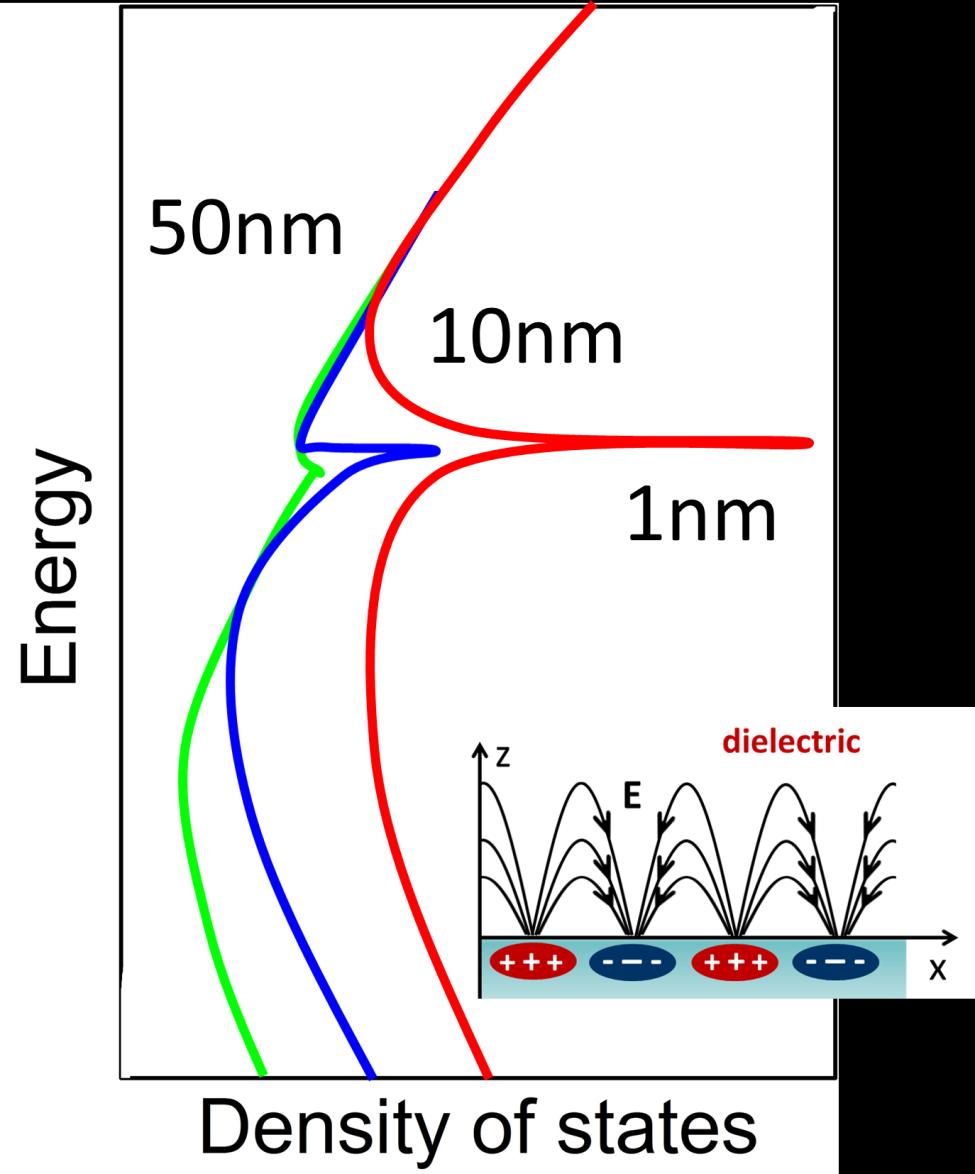
21 Transformation of the iso-frequency surface results in DOS sculpting
22 SPP waves generate highmomentum photons k 0 2 k k 2 0 E x
23 SPP waves generate highmomentum photons k 0 2 k k 2 0 k E x
24 Optical power flows in opposite directions along the M-D interface 1 S R e E H 2 * 2 S xˆ A e k 2 z Z=0 E x S xˆ A e k z 1
25 Optical power flows in opposite directions along the M-D interface 1 S R e E H 2 * Z=0 Singular & Chiral Nano-Plasmonics (Boriskina & Zheludev Eds.) Pan Stanford, 2014
26 Instantaneous powerflow features vortices that recycle energy across the interface S 1 R e E H 1 R e E H e 2 2 * i t S in Z=0 Singular & Chiral Nano-Plasmonics (Boriskina & Zheludev Eds.) Pan Stanford, 2014
27 Local k-vector is tangential to the powerflow streamlines S in Z=0 Singular & Chiral Nano-Plasmonics (Boriskina & Zheludev Eds.) Pan Stanford, 2014


28 Vertical components cancel on average S in Z=0 Singular & Chiral Nano-Plasmonics (Boriskina & Zheludev Eds.) Pan Stanford, 2014
29 29 Vortex powerflow is behind tight light localization and high photon momentum of SPP waves


30 From one interface to many: hyperbolic metamaterials ε x =ε y ε z ><0 Momentum fixed photon energy k Dispersion 2 2 c c k k k x y z k k k x y z S.V. Boriskina et al, Plasmonic materials for energy: from physics to applications, Mater. Today, 2013


31 Dispersion characteristics & DOS of a multi-layer stack 31 S.V. Boriskina et al, Plasmonic materials for energy: from physics to applications, Mater. Today, 2013
32 32 What is the local field topology behind a global topological phase transition in metamaterials?
 Pan Stanford, 2014 Optical tornadoes change energy density in hyperbolic")
33 Singular & Chiral Nano-Plasmonics (Boriskina & Zheludev Eds.) Pan Stanford, 2014 Optical tornadoes change energy density in hyperbolic metamaterials 33
 Pan Stanford, 2014 Optical tornadoes change energy density in hyperbolic")
34 Singular & Chiral Nano-Plasmonics (Boriskina & Zheludev Eds.) Pan Stanford, 2014 Optical tornadoes change energy density in hyperbolic metamaterials 34
 Pan Stanford, 2014 Optical tornadoes change energy density in hyperbolic")
35 Singular & Chiral Nano-Plasmonics (Boriskina & Zheludev Eds.) Pan Stanford, 2014 Optical tornadoes change energy density in hyperbolic metamaterials 35
 Pan Stanford, 2014 Optical tornadoes change energy density in hyperbolic")
36 Singular & Chiral Nano-Plasmonics (Boriskina & Zheludev Eds.) Pan Stanford, 2014 Optical tornadoes change energy density in hyperbolic metamaterials 36
 Pan Stanford, 2014 Optical tornadoes change energy density in hyperbolic")
37 Singular & Chiral Nano-Plasmonics (Boriskina & Zheludev Eds.) Pan Stanford, 2014 Optical tornadoes change energy density in hyperbolic metamaterials 37
 Pan Stanford, 2014 Optical tornadoes change energy density in hyperbolic")
38 Singular & Chiral Nano-Plasmonics (Boriskina & Zheludev Eds.) Pan Stanford, 2014 Optical tornadoes change energy density in hyperbolic metamaterials 38
39 Singular & Chiral Nano-Plasmonics (Boriskina & Zheludev Eds.) Pan Stanford, 2014 Optical tornadoes change energy density in hyperbolic metamaterials 39
 Pan Stanford, 2014 Optical tornadoes change energy density in hyperbolic")
40 Singular & Chiral Nano-Plasmonics (Boriskina & Zheludev Eds.) Pan Stanford, 2014 Optical tornadoes change energy density in hyperbolic metamaterials 40
 Pan Stanford, 2014 Optical tornadoes change energy density in hyperbolic")
41 Singular & Chiral Nano-Plasmonics (Boriskina & Zheludev Eds.) Pan Stanford, 2014 Optical tornadoes change energy density in hyperbolic metamaterials 41
42 42 Local optical tornadoes are behind plasmonic field localization and topological transitions in metamaterials
43 43 Can we design custom-tailored vortex-trapping nanostructures with low losses?


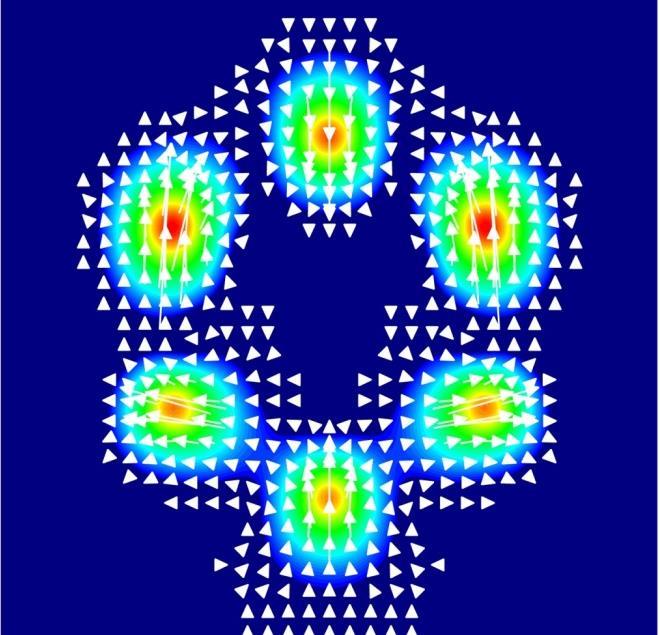
44 Yes we can - by strategically positioning obstacles in the light flow path 44 Zero intensity S.V. Boriskina & B.M. Reinhard, Nanoscale, 4, 76-90, 2012
45 Example of a vortex-pinning nanostructure nm radius Au nanoparticles S.V. Boriskina & B.M. Reinhard, Nanoscale, 4, (2012) W. Ahn, S.V. Boriskina, et al, Nano Lett. 12, (2012)
46 Example of a vortex-pinning nanostructure nm radius Au nanoparticles S.V. Boriskina & B.M. Reinhard, Nanoscale, 4, (2012) W. Ahn, S.V. Boriskina, et al, Nano Lett. 12, (2012)


 W.")

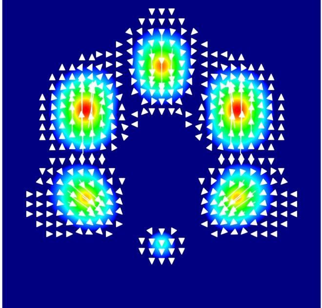
47 Optical energy is circulating outside the metal volume! 47 S.V. Boriskina & B.M. Reinhard, Nanoscale, 4, (2012) W. Ahn, S.V. Boriskina, et al, Nano Lett. 12, (2012)


48 What is the origin of the strong field enhancement? 48
49 Optical vortices generate local velocity fields 49 compressible fluid potential steadystate flow local convective acceleration possible v ( r ) v ( r ) V ( r ) r Tangential velocity ~1/r
50 Photon fluid is convectively accelerated in the vortex velocity field 50 compressible fluid potential steadystate flow local convective acceleration possible v ( r ) v ( r ) V ( r )

51 and when threaded through nanoscale gaps, generates hydraulic jumps - areas of high field intensity 51

52 and when threaded through nanoscale gaps, generates hydraulic jumps - areas of high field intensity 52

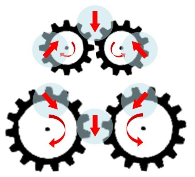
53 Vortex-pinning nanostructures are photonic analogs of turbopumps 53
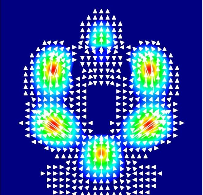
54 Optical vortices can be moved and stretched by repositioning the obstacles 54
55 Tunable or broadband light trapping possible 55
 Adv. Mat.")
56 E-beam SERS platforms fabricated with vortex-trapping VNTs surfaces Nano Lett. 12, (2012) Adv. Mat., 25(1), , 2013

57 Reconfigurable vortex transmissions S.V. Boriskina & B.M. Reinhard, Nanoscale, 4, 76-90, 2012


58 58 Nanoscale light switching S.V. Boriskina & B.M. Reinhard, Opt. Express, vol. 19, no. 22, pp , 2011
59 59 Nanoscale light switching S.V. Boriskina & B.M. Reinhard, Opt. Express, vol. 19, no. 22, pp , 2011

60 60 Nanoscale light switching S.V. Boriskina & B.M. Reinhard, Opt. Express, vol. 19, no. 22, pp , 2011

61 61 Nanoscale light switching S.V. Boriskina & B.M. Reinhard, Opt. Express, vol. 19, no. 22, pp , 2011

62 62 Nanoscale light switching S.V. Boriskina & B.M. Reinhard, Opt. Express, vol. 19, no. 22, pp , 2011
63 Advantages of the hydrodynamicsinspired design approach Optical chip High-Q (narrow linewidth) modes with high field intensity in sub-wavelength device footprints
64 Advantages of the hydrodynamicsinspired design approach Hydrodynamic picture of conventionally-designed optical chip High-Q (narrow linewidth) modes with high field intensity in sub-wavelength device footprints


65 Advantages of the hydrodynamicsinspired design approach Hydrodynamic picture of vortex-pinning optical chip High-Q (narrow linewidth) modes with high field intensity in sub-wavelength device footprints
66 Conclusions and outlook New way of designing light absorbers & routers via the hydrodynamic analogy Higher field concentration than traditional schemes based on constructive interference Strong energy flow outside of the metal volume of nanoparticles possible PV applications


67 Acknowledgements Prof. Gang Chen & MIT NanoEngineering group 67 Funding: Students & Colleagues: Collaborations & Discussions: Prof. Bjoern Reinhard, Boston University Dr. Anton Desyatnikov, Australian National University

, 22305-22315, 2011 Read")


68 Nanoscale, 4, 76-90, 2012 Nano Lett. 12, , 2012 Adv. Mat., 25(1), , 2013 Opt. Express 19(22), , 2011 Read more: Plasmonics with a twist: taming optical tornadoes on the nanoscale, to appear in Plasmonics: Theory & Applications, T.V. Shahbazyan & M.I. Stockman Eds., Springer 2012
Local field topology behind light localization and metamaterial topological transitions
 Chapter Eight Local field topology behind light localization and metamaterial topological transitions Jonathan Tong, Alvin Mercedes, Gang Chen*, and Svetlana V. Boriskina # Department of Mechanical Engineering,
Wednesday 3 September Session 3: Metamaterials Theory (16:15 16:45, Huxley LT308)
") Session 3: Metamaterials Theory (16:15 16:45, Huxley LT308) (invited) TBC Session 3: Metamaterials Theory (16:45 17:00, Huxley LT308) Light trapping states in media with longitudinal electric waves D McArthur,
Session 3: Metamaterials Theory (16:15 16:45, Huxley LT308) (invited) TBC Session 3: Metamaterials Theory (16:45 17:00, Huxley LT308) Light trapping states in media with longitudinal electric waves D McArthur,
High temperature plasmonics: Narrowband, tunable, nearfield. thermal sources
 High temperature plasmonics: Narrowband, tunable, nearfield thermal sources Yu Guo, S. Molesky, C. Cortes and Zubin Jacob * Department of Electrical and Computer Engineering, University of Alberta, Edmonton,
Sub-wavelength electromagnetic structures
 Sub-wavelength electromagnetic structures Shanhui Fan, Z. Ruan, L. Verselegers, P. Catrysse, Z. Yu, J. Shin, J. T. Shen, G. Veronis Ginzton Laboratory, Stanford University http://www.stanford.edu/group/fan
PLASMONICS/METAMATERIALS
 PLASMONICS/METAMATERIALS Interconnects Optical processing of data Subwavelength confinement Electrodes are in place Coupling to other on-chip devices Combination of guiding, detection, modulation, sensing
Effect of nonlinearity on wave scattering and localization. Yuri S. Kivshar
 Effect of nonlinearity on wave scattering and localization Yuri S. Kivshar Nonlinear Physics Centre, Australian National University, Canberra, Australia St. Petersburg University of Information Technologies,
Understanding Nanoplasmonics. Greg Sun University of Massachusetts Boston
 Understanding Nanoplasmonics Greg Sun University of Massachusetts Boston Nanoplasmonics Space 100pm 1nm 10nm 100nm 1μm 10μm 100μm 1ns 100ps 10ps Photonics 1ps 100fs 10fs 1fs Time Surface Plasmons Surface
Lecture 10: Surface Plasmon Excitation. 5 nm
 Excitation Lecture 10: Surface Plasmon Excitation 5 nm Summary The dispersion relation for surface plasmons Useful for describing plasmon excitation & propagation This lecture: p sp Coupling light to surface
Surface plasmon waveguides
 Surface plasmon waveguides Introduction Size Mismatch between Scaled CMOS Electronics and Planar Photonics Photonic integrated system with subwavelength scale components CMOS transistor: Medium-sized molecule
Quantum Information Processing with Electrons?
 Quantum Information Processing with 10 10 Electrons? René Stock IQIS Seminar, October 2005 People: Barry Sanders Peter Marlin Jeremie Choquette Motivation Quantum information processing realiations Ions
Light trapping in thin-film solar cells: the role of guided modes
 Light trapping in thin-film solar cells: the role of guided modes T. Søndergaard *, Y.-C. Tsao, T. G. Pedersen, and K. Pedersen Department of Physics and Nanotechnology, Aalborg University, Skjernvej 4A,
A Study on the Suitability of Indium Nitride for Terahertz Plasmonics
 A Study on the Suitability of Indium Nitride for Terahertz Plasmonics Arjun Shetty 1*, K. J. Vinoy 1, S. B. Krupanidhi 2 1 Electrical Communication Engineering, Indian Institute of Science, Bangalore,
Copyright. Francesco Monticone Topological Embedded Eigenstates
 Copyright The use of this work is restricted solely for academic purposes. The author of this work owns the copyright and no reproduction in any form is permitted without written permission by the author.
Nanomaterials and their Optical Applications
 Nanomaterials and their Optical Applications Winter Semester 2013 Lecture 02 rachel.grange@uni-jena.de http://www.iap.uni-jena.de/multiphoton Lecture 2: outline 2 Introduction to Nanophotonics Theoretical
New Aspects of Old Equations: Metamaterials and Beyond (Part 2) 신종화 KAIST 물리학과
 신종화 KAIST 물리학과") New Aspects of Old Equations: Metamaterials and Beyond (Part 2) 신종화 KAIST 물리학과 Metamaterial Near field Configuration in Periodic Structures New Material Material and Metamaterial Material Metamaterial
New Aspects of Old Equations: Metamaterials and Beyond (Part 2) 신종화 KAIST 물리학과 Metamaterial Near field Configuration in Periodic Structures New Material Material and Metamaterial Material Metamaterial
Nanoscale optical circuits: controlling light using localized surface plasmon resonances
 Nanoscale optical circuits: controlling light using localized surface plasmon resonances T. J. Davis, D. E. Gómez and K. C. Vernon CSIRO Materials Science and Engineering Localized surface plasmon (LSP)
Surface plasmon polariton propagation around bends at a metal-dielectric interface
 Surface plasmon polariton propagation around bends at a metal-dielectric interface Keisuke Hasegawa, Jens U. Nöckel and Miriam Deutsch Oregon Center for Optics, 1274 University of Oregon, Eugene, OR 97403-1274
Controlling Fano lineshapes in plasmon-mediated light coupling into a substrate
 Controlling Fano lineshapes in plasmon-mediated light coupling into a substrate P. Spinelli,* C. van Lare, E. Verhagen, and A. Polman Center for Nanophotonics, FOM Institute AMOLF Science Park, 98 XG,
Losses in Plasmonics: from mitigating energy dissipation to embracing lossenabled
 Losses in Plasmonics: from mitigating energy dissipation to embracing lossenabled functionalities SVETLANA V. BORISKINA, * THOMAS COOPER, LINGPING ZENG, GEORGE NI, JONATHAN K. TONG, YOICHIRO TSURIMAKI,
Supporting Information
 Supporting Information Light emission near a gradient metasurface Leonard C. Kogos and Roberto Paiella Department of Electrical and Computer Engineering and Photonics Center, Boston University, Boston,
Liquid Crystals IAM-CHOON 1(1100 .,4 WILEY 2007 WILEY-INTERSCIENCE A JOHN WILEY & SONS, INC., PUBLICATION. 'i; Second Edition. n z
 Liquid Crystals Second Edition IAM-CHOON 1(1100.,4 z 'i; BICENTCNNIAL 1 8 0 7 WILEY 2007 DICENTENNIAL n z z r WILEY-INTERSCIENCE A JOHN WILEY & SONS, INC., PUBLICATION Contents Preface xiii Chapter 1.
Introduction. Chapter Optics at the Nanoscale
 Chapter 1 Introduction 1.1 Optics at the Nanoscale The interaction of light with matter is one of the most significant processes on the planet, forming the basis of some of the most famous scientific discoveries
Gravitational field around blackhole induces photonic spin-orbit interaction that twists. light
 Gravitational field around blackhole induces photonic spin-orbit interaction that twists light Deng Pan, Hong-Xing Xu ǂ School of Physics and Technology, Wuhan University, Wuhan 430072, China Corresponding
EPSILON-NEAR-ZERO (ENZ) AND MU-NEAR-ZERO (MNZ) MATERIALS
 AND MU-NEAR-ZERO (MNZ) MATERIALS") EPSILON-NEAR-ZERO (ENZ) AND MU-NEAR-ZERO (MNZ) MATERIALS SARAH NAHAR CHOWDHURY PURDUE UNIVERSITY 1 Basics Design ENZ Materials Lumped circuit elements Basics Decoupling Direction emission Tunneling Basics
EPSILON-NEAR-ZERO (ENZ) AND MU-NEAR-ZERO (MNZ) MATERIALS SARAH NAHAR CHOWDHURY PURDUE UNIVERSITY 1 Basics Design ENZ Materials Lumped circuit elements Basics Decoupling Direction emission Tunneling Basics
Nanoscale Systems for Opto-Electronics
 Nanoscale Systems for Opto-Electronics 675 PL intensity [arb. units] 700 Wavelength [nm] 650 625 600 5µm 1.80 1.85 1.90 1.95 Energy [ev] 2.00 2.05 Nanoscale Systems for Opto-Electronics Lecture 1 Dozent:
From optical graphene to topological insulator
 From optical graphene to topological insulator Xiangdong Zhang Beijing Institute of Technology (BIT), China zhangxd@bit.edu.cn Collaborator: Wei Zhong (PhD student, BNU) Outline Background: From solid
Nanophotonics: solar and thermal applications
 Nanophotonics: solar and thermal applications Shanhui Fan Ginzton Laboratory and Department of Electrical Engineering Stanford University http://www.stanford.edu/~shanhui Nanophotonic Structures Photonic
Plasmonic fractals: ultrabroadband light trapping in thin film solar cells by a Sierpinski nanocarpet
 Plasmonic fractals: ultrabroadband light trapping in thin film solar cells by a Sierpinski nanocarpet Hanif Kazerooni 1, Amin Khavasi, 2,* 1. Chemical Engineering Faculty, Amirkabir University of Technology
Self-assembled nanostructures for antireflection optical coatings
 Self-assembled nanostructures for antireflection optical coatings Yang Zhao 1, Guangzhao Mao 2, and Jinsong Wang 1 1. Deaprtment of Electrical and Computer Engineering 2. Departmentof Chemical Engineering
Propagation of Surface Plasmon Polariton in the Single Interface of Gallium Lanthanum Sulfide and Silver
 PHOTONIC SENSORS / Vol., No., : 58 6 Propagation of Surface Plasmon Polariton in the Single Interface of Gallium Lanthanum Sulfide and Silver Rakibul Hasan SAGOR, Md. Ghulam SABER *, and Md. Ruhul AMIN
Left-handed materials: Transfer matrix method studies
 Left-handed materials: Transfer matrix method studies Peter Markos and C. M. Soukoulis Outline of Talk What are Metamaterials? An Example: Left-handed Materials Results of the transfer matrix method Negative
Self-trapped optical beams: From solitons to vortices
 Self-trapped optical beams: From solitons to vortices Yuri S. Kivshar Nonlinear Physics Centre, Australian National University, Canberra, Australia http://wwwrsphysse.anu.edu.au/nonlinear/ Outline of today
Seminars in Nanosystems - I
 Seminars in Nanosystems - I Winter Semester 2011/2012 Dr. Emanuela Margapoti Emanuela.Margapoti@wsi.tum.de Dr. Gregor Koblmüller Gregor.Koblmueller@wsi.tum.de Seminar Room at ZNN 1 floor Topics of the
Nanomaterials and their Optical Applications
 Nanomaterials and their Optical Applications Winter Semester 2012 Lecture 04 rachel.grange@uni-jena.de http://www.iap.uni-jena.de/multiphoton Lecture 4: outline 2 Characterization of nanomaterials SEM,
Superconductivity Induced Transparency
 Superconductivity Induced Transparency Coskun Kocabas In this paper I will discuss the effect of the superconducting phase transition on the optical properties of the superconductors. Firstly I will give
Supplementary Figure 1 Schematics of an optical pulse in a nonlinear medium. A Gaussian optical pulse propagates along z-axis in a nonlinear medium
 Supplementary Figure 1 Schematics of an optical pulse in a nonlinear medium. A Gaussian optical pulse propagates along z-axis in a nonlinear medium with thickness L. Supplementary Figure Measurement of
Origin of Optical Enhancement by Metal Nanoparticles. Greg Sun University of Massachusetts Boston
 Origin of Optical Enhancement by Metal Nanoparticles Greg Sun University of Massachusetts Boston Nanoplasmonics Space 100pm 1nm 10nm 100nm 1μm 10μm 100μm Photonics 1ns 100ps 10ps 1ps 100fs 10fs 1fs Time
Metamaterial-Induced
 Metamaterial-Induced Sharp ano Resonances and Slow Light Nikitas Papasimakis and Nikolay I. Zheludev Inspired by the study of atomic resonances, researchers have developed a new type of metamaterial. Their
Broadband Absorption in the Cavity Resonators with Changed Order
 Broadband Absorption in the Cavity Resonators with Changed Order Agata Roszkiewicz Institute of Fundamental Technological Research, Polish Academy of Sciences, Adolfa Pawińskiego 5b, 02-106 Warsaw, Poland
Gradient-index metamaterials and spoof surface plasmonic waveguide
 Gradient-index metamaterials and spoof surface plasmonic waveguide Hui Feng Ma State Key Laboratory of Millimeter Waves Southeast University, Nanjing 210096, China City University of Hong Kong, 11 October
Near-perfect modulator for polarization state of light
 Journal of Nanophotonics, Vol. 2, 029504 (11 November 2008) Near-perfect modulator for polarization state of light Yi-Jun Jen, Yung-Hsun Chen, Ching-Wei Yu, and Yen-Pu Li Department of Electro-Optical
7. Localized surface plasmons (Particle plasmons)
") 7. Localized surface plasmons (Particle plasmons) ( Plasmons in metal nanostructures, Dissertation, University of Munich by Carsten Sonnichsen, 2001) Lycurgus cup, 4th century (now at the British Museum,
7. Localized surface plasmons (Particle plasmons) ( Plasmons in metal nanostructures, Dissertation, University of Munich by Carsten Sonnichsen, 2001) Lycurgus cup, 4th century (now at the British Museum,
Nonlinear Optics and Gap Solitons in Periodic Photonic Structures
 Nonlinear Optics and Gap Solitons in Periodic Photonic Structures Yuri Kivshar Nonlinear Physics Centre Research School of Physical Sciences and Engineering Australian National University Perspectives
The Dielectric Function of a Metal ( Jellium )
") The Dielectric Function of a Metal ( Jellium ) Total reflection Plasma frequency p (10 15 Hz range) Why are Metals Shiny? An electric field cannot exist inside a metal, because metal electrons follow the
The Dielectric Function of a Metal ( Jellium ) Total reflection Plasma frequency p (10 15 Hz range) Why are Metals Shiny? An electric field cannot exist inside a metal, because metal electrons follow the
Magnetoplasmonics: fundamentals and applications
 Antonio García-Martín http://www.imm-cnm.csic.es/magnetoplasmonics Instituto de Microelectrónica de Madrid Consejo Superior de Investigaciones Científicas Magnetoplasmonics: fundamentals and applications
Optical nonlocality induced Zitterbewegung near the Dirac point in metal-dielectric multilayer metamaterials
 Optical nonlocality induced Zitterbewegung near the Dirac point in metal-dielectric multilayer metamaterials Lei Sun, 1 Jie Gao, 2 and Xiaodong Yang 3 1 Department of Mechanical and Aerospace Engineering,
SURFACE PLASMONS AND THEIR APPLICATIONS IN ELECTRO-OPTICAL DEVICES
 SURFACE PLASMONS AND THEIR APPLICATIONS IN ELECTRO-OPTICAL DEVICES Igor Zozouleno Solid State Electronics Department of Science and Technology Linöping University Sweden igozo@itn.liu.se http://www.itn.liu.se/meso-phot
Metamaterials & Plasmonics
 Metamaterials & Plasmonics Exploring the Impact of Rotating Rectangular Plasmonic Nano-hole Arrays on the Transmission Spectra and its Application as a Plasmonic Sensor. Abstract Plasmonic nano-structures
Mathematical Pattern of Plasmon Surface Selection Rules According to DrudeModel
 International Journal of Recent Research and Review, Vol. X, Issue 1, March 2017 ISSN 2277 8322 Mathematical Pattern of Plasmon Surface Selection Rules According to DrudeModel Raad A. Khamis 1,Hussam N.
MODAL ANALYSIS OF EXTRAORDINARY TRANSMISSION THROUGH AN ARRAY OF SUBWAVELENGTH SLITS
 Progress In Electromagnetics Research, PIER 79, 59 74, 008 MODAL ANALYSIS OF EXTRAORDINARY TRANSMISSION THROUGH AN ARRAY OF SUBWAVELENGTH SLITS G. Ghazi and M. Shahabadi Center of Excellence for Applied
Spring 2009 EE 710: Nanoscience and Engineering
 Spring 009 EE 710: Nanoscience and Engineering Part 10: Surface Plasmons in Metals Images and figures supplied from Hornyak, Dutta, Tibbals, and Rao, Introduction to Nanoscience, CRC Press Boca Raton,
Localized surface plasmons (Particle plasmons)
") Localized surface plasmons (Particle plasmons) ( Plasmons in metal nanostructures, Dissertation, University of Munich by Carsten Sonnichsen, 2001) Lycurgus cup, 4th century (now at the British Museum,
Localized surface plasmons (Particle plasmons) ( Plasmons in metal nanostructures, Dissertation, University of Munich by Carsten Sonnichsen, 2001) Lycurgus cup, 4th century (now at the British Museum,
Rezonanse typu spin-orbit w meta-materiałowych elementach nanofotoniki Spin-orbit resonances in meta-material elements of nanophotonics
 Rezonanse typu spin-orbit w meta-materiałowych elementach nanofotoniki Spin-orbit resonances in meta-material elements of nanophotonics Wojciech Nasalski Zespół Badawczy Nanofotoniki Instytut Podstawowych
Plasmonics: elementary excitation of a plasma (gas of free charges) nano-scale optics done with plasmons at metal interfaces
 nano-scale optics done with plasmons at metal interfaces") Plasmonics Plasmon: Plasmonics: elementary excitation of a plasma (gas of free charges) nano-scale optics done with plasmons at metal interfaces Femius Koenderink Center for Nanophotonics AMOLF, Amsterdam
Plasmonics Plasmon: Plasmonics: elementary excitation of a plasma (gas of free charges) nano-scale optics done with plasmons at metal interfaces Femius Koenderink Center for Nanophotonics AMOLF, Amsterdam
Lecture 10 Light-Matter Interaction Part 4 Surface Polaritons 2. EECS Winter 2006 Nanophotonics and Nano-scale Fabrication P.C.
 Lecture 10 Light-Matter Interaction Part 4 Surface Polaritons 2 EECS 598-002 Winter 2006 Nanophotonics and Nano-scale Fabrication P.C.Ku Schedule for the rest of the semester Introduction to light-matter
Plasmonic nanoguides and circuits
 Plasmonic nanoguides and circuits Introduction: need for plasmonics? Strip SPPs Cylindrical SPPs Gap SPP waveguides Channel plasmon polaritons Dielectric-loaded SPP waveguides PLASMOCOM 1. Intro: need
Plasmonic Photovoltaics Harry A. Atwater California Institute of Technology
 Plasmonic Photovoltaics Harry A. Atwater California Institute of Technology Surface plasmon polaritons and localized surface plasmons Plasmon propagation and absorption at metal-semiconductor interfaces
Routing of Deep-Subwavelength Optical Beams and Images without Reflection and Diffraction Using Infinitely Anisotropic Metamaterials
 Peter B. Catrysse * and Shanhui Fan Routing of Deep-Subwavelength Optical Beams and Images without Reflection and Diffraction Using Infinitely Anisotropic Metamaterials Media that are described by extreme
Taking cascaded plasmonic field enhancement to the ultimate limit in silver nanoparticle dimers S. Toroghi* a, P. G. Kik a,b
 Taking cascaded plasmonic field enhancement to the ultimate limit in silver nanoparticle dimers S. Toroghi* a, P. G. Kik a,b a CREOL, The College of Optics and Photonics, University of Central Florida,
Exploiting duality using metamaterials
 Exploiting duality using metamaterials Jensen Li School of Physics and Astronomy, University of Birmingham, UK Jan 12, 2015 Metamaterials with magnetic response Interesting physics by pairing up electric
Energy transport in metal nanoparticle plasmon waveguides
 Energy transport in metal nanoparticle plasmon waveguides Stefan A. Maier, Pieter G. Kik, and Harry A. Atwater California Institute of Technology Thomas J. Watson Laboratory of Applied Physics, Pasadena,
A Dielectric Invisibility Carpet
 A Dielectric Invisibility Carpet Jensen Li Prof. Xiang Zhang s Research Group Nanoscale Science and Engineering Center (NSEC) University of California at Berkeley, USA CLK08-09/22/2008 Presented at Center
Optical Trapping Force on a Plasmonic Substrate
 Yu Pan Master of Science Thesis Supervisor: Prof. Min Yan(KTH) Examiner: Prof. Min Qiu(KTH) TRITA-ICT-EX-2012: 107 Abstract Optical trapping is currently widely applied in the field of biotechnology, in
Light-Switching-Light Optical Transistor based on Metallic Nanoparticle Cross-chains Geometry Incorporating Kerr Nonlinearity
 Articletype: Annalen der Physik Light-Switching-Light Optical Transistor based on Metallic Nanoparticle Cross-chains Geometry Incorporating Kerr Nonlinearity Fathi AbdelMalek 1, Walid Aroua 1, Shyqyri
Natallia Strekal. Plasmonic films of noble metals for nanophotonics
 Natallia Strekal Plasmonic films of noble metals for nanophotonics The aim of our investigation is the mechanisms of light interactions with nanostructure and High Tech application in the field of nanophotonics
Name Final Exam May 1, 2017
 Name Final Exam May 1, 217 This test consists of five parts. Please note that in parts II through V, you can skip one question of those offered. Some possibly useful formulas appear below. Constants, etc.
OPTICAL PROPERTIES of Nanomaterials
 OPTICAL PROPERTIES of Nanomaterials Advanced Reading Optical Properties and Spectroscopy of Nanomaterials Jin Zhong Zhang World Scientific, Singapore, 2009. Optical Properties Many of the optical properties
Chapter 5. Photonic Crystals, Plasmonics, and Metamaterials
 Chapter 5. Photonic Crystals, Plasmonics, and Metamaterials Reading: Saleh and Teich Chapter 7 Novotny and Hecht Chapter 11 and 12 1. Photonic Crystals Periodic photonic structures 1D 2D 3D Period a ~
1. Reminder: E-Dynamics in homogenous media and at interfaces
 0. Introduction 1. Reminder: E-Dynamics in homogenous media and at interfaces 2. Photonic Crystals 2.1 Introduction 2.2 1D Photonic Crystals 2.3 2D and 3D Photonic Crystals 2.4 Numerical Methods 2.5 Fabrication
A Highly Tunable Sub-Wavelength Chiral Structure for Circular Polarizer
 A Highly Tunable Sub-Wavelength Chiral Structure for Circular Polarizer Menglin. L. N. Chen 1, Li Jun Jiang 1, Wei E. I. Sha 1 and Tatsuo Itoh 2 1 Dept. Of EEE, The University Of Hong Kong 2 EE Dept.,
ABSTRACT 1. INTRODUCTION
 Cascaded plasmon resonances multi-material nanoparticle trimers for extreme field enhancement S. Toroghi a, Chatdanai Lumdee a, and P. G. Kik* a CREOL, The College of Optics and Photonics, University of
Surface Plasmon Amplification by Stimulated Emission of Radiation. By: Jonathan Massey-Allard Graham Zell Justin Lau
 Surface Plasmon Amplification by Stimulated Emission of Radiation By: Jonathan Massey-Allard Graham Zell Justin Lau Surface Plasmons (SPs) Quanta of electron oscillations in a plasma. o Electron gas in
Terahertz antireflection coating enabled by a subwavelength metallic mesh capped with a thin dielectric film
 Invited Paper Terahertz antireflection coating enabled by a subwavelength metallic mesh capped with a thin dielectric film Li Huang 1*, Beibei Zeng 2, Chun-Chieh Chang 2 and Hou-Tong Chen 2* 1 Physics
Nanomaterials and their Optical Applications
 Nanomaterials and their Optical Applications Winter Semester 2012 Lecture 08 rachel.grange@uni-jena.de http://www.iap.uni-jena.de/multiphoton Outline: Photonic crystals 2 1. Photonic crystals vs electronic
PlasmonicsÐA Route to Nanoscale Optical Devices**
 PlasmonicsÐA Route to Nanoscale Optical Devices** By Stefan A. Maier, Mark. Brongersma, Pieter G. Kik, Sheffer Meltzer, Ari A. G. Requicha, and Harry A. Atwater* he further integration of optical devices
Tunable plasmon resonance of a touching gold cylinder arrays
 J. At. Mol. Sci. doi: 10.4208/jams.091511.101811a Vol. 3, No. 3, pp. 252-261 August 2012 Tunable plasmon resonance of a touching gold cylinder arrays Geng-Hua Yan a, Yan-Ying Xiao a, Su-Xia Xie b, and
Surface Plasmon Polariton Assisted Metal-Dielectric Multilayers as Passband Filters for Ultraviolet Range
 Vol. 112 (2007) ACTA PHYSICA POLONICA A No. 5 Proceedings of the International School and Conference on Optics and Optical Materials, ISCOM07, Belgrade, Serbia, September 3 7, 2007 Surface Plasmon Polariton
Nanophysics: Main trends
 Nano-opto-electronics Nanophysics: Main trends Nanomechanics Main issues Light interaction with small structures Molecules Nanoparticles (semiconductor and metallic) Microparticles Photonic crystals Nanoplasmonics
Quantum optics and metamaterials. Janne Ruostekoski Mathematics & Centre for Photonic Metamaterials University of Southampton
 Quantum optics and metamaterials Janne Ruostekoski Mathematics & Centre for Photonic Metamaterials University of Southampton Motivation Quantum optics a well-developed field for studying interaction of
NANO/MICROSCALE HEAT TRANSFER
 NANO/MICROSCALE HEAT TRANSFER Zhuomin M. Zhang Georgia Institute of Technology Atlanta, Georgia New York Chicago San Francisco Lisbon London Madrid Mexico City Milan New Delhi San Juan Seoul Singapore
Optimizing the performance of metal-semiconductor-metal photodetectors by embedding nanoparticles in the absorption layer
 Journal of Electrical and Electronic Engineering 2015; 3(2-1): 78-82 Published online February 10, 2015 (http://www.sciencepublishinggroup.com/j/jeee) doi: 10.11648/j.jeee.s.2015030201.27 ISSN: 2329-1613
Shaping the Beam of Light in Nanometer Scales: A Yagi-Uda Nanoantenna in Optical Domain
 Shaping the Beam of Light in Nanometer Scales: A Yagi-Uda Nanoantenna in Optical Domain Jingjing Li, Alessandro Salandrino, and Nader Engheta* University of Pennsylvania Department of Electrical and Systems
Plasmonics. The long wavelength of light ( μm) creates a problem for extending optoelectronics into the nanometer regime.
 creates a problem for extending optoelectronics into the nanometer regime.") Plasmonics The long wavelength of light ( μm) creates a problem for extending optoelectronics into the nanometer regime. A possible way out is the conversion of light into plasmons. They have much shorter
Plasmonics The long wavelength of light ( μm) creates a problem for extending optoelectronics into the nanometer regime. A possible way out is the conversion of light into plasmons. They have much shorter
Biosensing based on slow plasmon nanocavities
 iosensing based on slow plasmon nanocavities. Sepulveda, 1, Y. Alaverdyan,. rian, M. Käll 1 Nanobiosensors and Molecular Nanobiophysics Group Research Center on Nanoscience and Nanotechnolog (CIN)CSIC-ICN
Enhancing and suppressing radiation with some permeability-near-zero structures
 Enhancing and suppressing radiation with some permeability-near-zero structures Yi Jin 1,2 and Sailing He 1,2,3,* 1 Centre for Optical and Electromagnetic Research, State Key Laboratory of Modern Optical
Embedded metallic nanopatterns for enhanced optical absorption
 Embedded metallic nanopatterns for enhanced optical absorption Fan Ye, Michael J. Burns, Michael J. Naughton* Department of Physics, Boston College, Chestnut Hill MA 02467 ABSTRACT Novel metallic nanopatterns
Peter Hertel. University of Osnabrück, Germany. Lecture presented at APS, Nankai University, China.
 University of Osnabrück, Germany Lecture presented at APS, Nankai University, China http://www.home.uni-osnabrueck.de/phertel Spring 2012 are metamaterials with strange optical properties structures with
Grating-coupled transmission-type surface plasmon resonance sensors based on dielectric and metallic gratings
 Grating-coupled transmission-type surface plasmon resonance sensors based on dielectric and metallic gratings Kyung Min Byun, 1 Sung June Kim, 1 and Donghyun Kim 2, * 1 School of Electrical Engineering
Substrate effect on aperture resonances in a thin metal film
 Substrate effect on aperture resonances in a thin metal film J. H. Kang 1, Jong-Ho Choe 1,D.S.Kim 2, Q-Han Park 1, 1 Department of Physics, Korea University, Seoul, 136-71, Korea 2 Department of Physics
File Name: Supplementary Information Description: Supplementary Figures, Supplementary Table, Supplementary Notes and Supplementary References
 Description of Supplementary Files File Name: Supplementary Information Description: Supplementary Figures, Supplementary Table, Supplementary Notes and Supplementary References Supplementary Figure 1.
Workshop on New Materials for Renewable Energy
 2286-6 Workshop on New Materials for Renewable Energy 31 October - 11 November 201 Metamaterials: Past, Present, and Future Nonlinear Physics Centre Research School of Physics and Engineering The Australian
Tooth-shaped plasmonic waveguide filters with nanometeric. sizes
 Tooth-shaped plasmonic waveguide filters with nanometeric sizes Xian-Shi LIN and Xu-Guang HUANG * Laboratory of Photonic Information Technology, South China Normal University, Guangzhou, 510006, China
Electromagnetic Absorption by Metamaterial Grating System
 PIERS ONLINE, VOL. 4, NO. 1, 2008 91 Electromagnetic Absorption by Metamaterial Grating System Xiaobing Cai and Gengkai Hu School of Science, Beijing Institute of Technology, Beijing 100081, China Abstract
Numerical Simulation of Light Propagation Through Composite and Anisotropic Media Using Supercomputers
 Moscow, Russia, September 25-26, 2017 Numerical Simulation of Light Propagation Through Composite and Anisotropic Media Using Supercomputers R.V. Galev, A.N. Kudryavtsev, S.I. Trashkeev Khristianovich
Finite element simulation of surface plasmon-polaritons: generation by edge effects, and resonance
 1 Matthias Maier May 18, Finite2017 element simulation of SPPs: edge effects and resonance Finite element simulation of surface plasmon-polaritons: generation by edge effects, and resonance Matthias Maier
Research on the Wide-angle and Broadband 2D Photonic Crystal Polarization Splitter
 Progress In Electromagnetics Research Symposium 2005, Hangzhou, China, August 22-26 551 Research on the Wide-angle and Broadband 2D Photonic Crystal Polarization Splitter Y. Y. Li, P. F. Gu, M. Y. Li,
Nanostrukturphysik (Nanostructure Physics)
") Nanostrukturphysik (Nanostructure Physics) Prof. Yong Lei & Dr. Yang Xu Fachgebiet 3D-Nanostrukturierung, Institut für Physik Contact: yong.lei@tu-ilmenau.de; yang.xu@tu-ilmenau.de Office: Unterpoerlitzer
Nanostrukturphysik (Nanostructure Physics) Prof. Yong Lei & Dr. Yang Xu Fachgebiet 3D-Nanostrukturierung, Institut für Physik Contact: yong.lei@tu-ilmenau.de; yang.xu@tu-ilmenau.de Office: Unterpoerlitzer
Simulations of nanophotonic waveguides and devices using COMSOL Multiphysics
 Presented at the COMSOL Conference 2010 China Simulations of nanophotonic waveguides and devices using COMSOL Multiphysics Zheng Zheng Beihang University 37 Xueyuan Road, Beijing 100191, China Acknowledgement
LECTURE 23: LIGHT. Propagation of Light Huygen s Principle
 LECTURE 23: LIGHT Propagation of Light Reflection & Refraction Internal Reflection Propagation of Light Huygen s Principle Each point on a primary wavefront serves as the source of spherical secondary
Observation of coupled plasmon-polariton modes of plasmon waveguides for electromagnetic energy transport below the diffraction limit
 Mat. Res. Soc. Symp. Proc. Vol. 722 2002 Materials Research Society Observation of coupled plasmon-polariton modes of plasmon waveguides for electromagnetic energy transport below the diffraction limit