Tooth-shaped plasmonic waveguide filters with nanometeric. sizes
|
|
|
- Liliana Bennett
- 5 years ago
- Views:
Transcription
1 Tooth-shaped plasmonic waveguide filters with nanometeric sizes Xian-Shi LIN and Xu-Guang HUANG * Laboratory of Photonic Information Technology, South China Normal University, Guangzhou, , China * Corresponding author: huangxg@scnu.edu.cn A novel nanometeric plasmonic filter in a tooth-shaped Metal-Insulator-Metal waveguide is proposed and demonstrated numerically. An analytic model based on the scattering matrix method is given. The result reveals that the single tooth-shaped filter has a wavelength filtering characteristic and an ultra-compact size in the length of a few hundred nanometers, compared to grating-like SPPs filters. Both analytic and simulation results show that the wavelength of the trough of the transmission has linear and nonlinear relationships with the tooth depth and the tooth width, respectively. The waveguide filter could be utilized to develop ultra-compact photonic filters for high integration. 008 Optical Society of America OCIS codes: , , ,
2 Surface Plasmons are waves that propagate along a metal-dielectric interface with an exponentially decaying field in the both sides [1,]. The unique properties of Surface Plasmon Plolaritons (SPPs) have shown the potential to overcome the diffraction limit in conventional optics, which could be utilized to achieve nano-scale photonic devices for high integration. Several different Metal-Insulator-Metal (MIM) waveguide structures based on SPPs have been numerically and/or experimentally demonstrated such as U-shaped waveguides [3], splitters [4], Y-shaped combiner [5], Multimode-Interferometers [6], couplers [7,8], M-Z interferometers [9,10], Bragg mirrors [11], and photonic bandgap structures [1]. To achieve wavelength filtering characteristics, SPPs Bragg reflectors and nanocavities have been proposed. They include the metal heterostructures constructed with several periodic slots vertically along a MIM waveguide [13,14], the Bragg grating fabricated by periodic modulating the thickness of thin metal stripes embedded in a insulator [15] and the periodic structure formed by changing alternately two kinds of the insulators with the same width [16] or different widths [17,18]. Lately, a high-order plasmonic Bragg reflector with a periodic modulation of the core index of the insulators [19], and a structure with periodic variation of the width of the insulator in MIM waveguide [0] have been proposed. Most of the structures mentioned above, however, have the period number of N > 9 with the total lengths over 4μm and beyond subwavelength-scale, which result in relatively high insertion loss of several db. In this letter, a nanoscale SPPs filter based on the MIM waveguide consisting of single rectangular tooth is proposed. The SPPs distributions and propagations are characterized by the method of Finite-Difference Time-Domain (FDTD), with perfect-matching-layer absorbing boundary conditions. An analytic model based on the scattering matrix method is derived to explain the filtering mechanism of the structure.
3 To begin with the dispersion relation of the fundamental TM mode in a MIM waveguide (shown in the inset of Fig. 1) is given by [15,1]: ε ik + = (1) z1 inkz εmkz1coth( w) 0, with k z1 and k z defined by momentum conservations: k ε k β, k ε k z1 = in 0 z = m 0 β. () Where εin and ε m are respectively dielectric constants of the insulator and the metal, k 0 =π/λ 0 is the free-space wave vector. The propagation constant β is represented as the effective index n eff =β/k 0 of the waveguide for SPPs. The real part of n eff of the slit waveguide as a function of the slit width at different wavelengths is shown in Fig. 1. It should be noted that the dependence of n eff on waveguide width is also suitable to the small part or region of the tooth waveguide with the tooth width of w t shown in Fig.. The imaginary part of n eff is referred to the propagation length which is defined as the length over which the power carried by the wave decays to 1/e of its initial value: L =λ /[4π Im(n )] spps 0 eff. In the calculation above and the following simulations, the insulator in all of the structures is assumed to be air ( ε in = 1 ), and the frequency-dependent complex relative permittivity of silver is characterized by Drude model: ε ( ω) = ε ω / ω( ω+ γ ). m p i 16 Hereω = Hz is the bulk plasma frequency, which represents the natural frequency of the p 13 oscillations of free conduction electrons. γ = Hz is the damping frequency of the oscillations, ω is the angular frequency of the incident electromagnetic radiation, ε stands for the dielectric constant at infinite angular frequency with the value of 3.7 [0]. The tooth-shaped waveguide filter is shown in Fig.. In the following FDTD simulations, the grid sizes in the x and z directions are chosen to be 5nm 5nm. The fundamental TM mode of 3
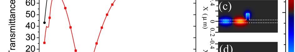
4 the plasmonic waveguide is excited by a dipole source. Two power monitors are respectively set at the points of P and Q to detect the incident and transmission fields for calculating the incident power of P in and the transmitted power of P out. The transmittance is defined to be T=P out /P in. The length of L is fixed to be 300nm, while the tooth width and depth are respectively w t =50nm and d=100nm. As shown in Fig. 3(a), the tooth-shaped waveguide is of a filtering function: A trough occurs at the free space wavelength nearly 784nm with the transmittance of ~0%. The maximum transmittance at the wavelengths longer than 1700nm is over 90%. The contour profiles of the field distributions around the tooth-shaped area at different wavelengths are shown in Figs. 3(b)- 3(d). The filtering structure is distinguished from the Bragg reflectors based on periodical heterostructure. The phenomenon above can be physically explained in the scattering matrix theory [3] as follows: E E out E = S E E E out in 1 1 in out in 3 3, (3) where r1 t1 s3 S t r s = s1 s1 r3, r i, t i and s i (i=1,,3) are respectively the reflection, transmission and splitting coefficients of a incident beam from Port i (i=1,,3), caused by the structure. E and E in i out i stand for the fields of incident and output beams at Port i, respectively. Using the fact that S = 1, one can obtain: rr+ tss rss tr=. (4)
5 in For the case of E = 0, one has E = te + se, (5) out in in in which in E 3 is given as follows: se E = s E exp( i φ ( λ ))(1 + r exp( i φ ( λ )) + r exp( i φ ( λ )) +...) = exp( i ( )) 1 exp( φλ ( )) φ λ, (6) in in in r3 i 4π where the phase delay φ( λ) = neff d +Δ ϕ( λ), and Δ ϕ( λ) is the phase-shift caused by the λ reflection on the air-silver surface. Combined Eq. (5) and Eq. (6), the output field at Port is derived as: sse E = t E + exp( iφ ( λ)), (7) 1 exp( φλ ( )) in out in r3 i Therefore, the transmittance T from Port 1 to Port is given by: out E ss 1 3 T t in 1 i E1 1 r3 exp( iφλ ( )) = = + exp( φλ ( )). (8) It can be seen from Eq. (8) that, if the phase satisfies φ( λ) = (m + 1) π (m=0,1, ), the two terms inside the absolute value sign on the right of the equation will cancel each other (as it can be seen in Fig. 3(c)), so that the transmittance T will become minimum. Therefore, the wavelength λ m of the trough of transmission is determined as follows: 4 neff d λm = Δϕ( λ) (m + 1) π. (9) 5
6 It can be seen that the wavelength λ m is linear to the tooth depth d, and depends on tooth width w t, through the somewhat inverse-proportion-like relationship between n eff and w t shown in Fig. 1. Figure 4(a) shows the transmission spectra of the waveguide filters with various tooth widths of w t. The maximum transmittance can reach 97%. Figure 4(b) shows the wavelength of the trough vs. the tooth width of w t. The primary trough of the transmission moves very significantly to short wavelength (blue-shift) with the increase of w t for w t <0nm. The shift rate rapidly becomes small after w t >0nm, and tends to be saturated when w t >00nm. As revealed in the Eq. (9), the above relationship between the trough position and w t mainly results from the contribution of the inverse-proportion-like dependence of n eff on w t. The change rate of Δn eff /Δw t within the tooth width of 0nm is much higher than that of Δn eff /Δw t after w t >0nm, as shown in Fig. 1 and Ref.13, and becomes finally saturated after w t >00nm. Obviously, tooth width w t should be chosen within the range of 0-00nm to avoid the critical behavior and the difficulty in fabrication process. Figure 5(a) shows the transmission spectra of the filters with different tooth depths of d. It is found that the wavelength of the trough shifts to long wavelength with the increasing of d. Figure 5(b) reveals that the wavelength of the trough has a linear relationship with the tooth depth, as our expectation in Eq. (9). Therefore, one can realize the filter function in various required wavelength with high performance, by changing the width or/and the depth of the tooth. For example, to obtain a filter with a trough at the wavelength of 1550nm, the structural parameters of w t =w=50nm and d=37.5nm can be chosen. In summary, a novel plasmonic waveguide filter constructed with a MIM structure engraved single rectangular tooth is investigated. The filter is of an ultra-compact size with a few hundreds of nanometers in length, and then low insertion loss. Moreover, it is promised to reduce 6
7 the difficulties in fabrication, comparing with previous grating-like heterostructures with a few micrometers in length. Our results suggest that the new structure could be utilized to develop plasmonic wavelength filters on flat metallic surfaces with extreme high integration for planar nanometeric photonic circuits. The authors acknowledge the financial support from the Natural Science Foundation of Guangdong Province, China (Grant No ). 7
8 References 1. H. Raether, Surface Plasmon on Smooth and Rough Surfaces and on Gratings (Springer- Verlag, Berlin, Germany, 1988).. W. L. Barnes, A. Dereux, and T. Ebbesen, "Surface plasmon subwavelength optics," Nature 44, (003). 3. T. Lee and S. Gray, "Subwavelength light bending by metal slit structures," Opt. Express 13, (005). 4. G. Veronis and S. Fan, "Bends and splitters in metal-dielectric-metal subwavelength plasmonic waveguides," Appl. Phys. Lett. 87, (005). 5. H. Gao, H. Shi, C. Wang, C. Du, X. Luo, Q. Deng, Y. Lv, X. Lin, and H. Yao, "Surface plasmon polariton propagation and combination in Y-shaped metallic channels," Opt. Express 13, (005). 6. Z. Han and S. He, "Multimode interference effect in plasmonic subwavelength waveguides and an ultra-compact power splitter," Opt. Commun. 78, (007). 7. T. Nikolajsen, K. Leosson and S. I. Bozhevolnyia, "Surface plasmon polariton based modulators and switches operating at telecom wavelengths," Appl. Phys. Lett. 85, 5833 (004). 8. H. Zhao, X. Huang and J. Huang, "Novel optical directional coupler based on surface plasmon polaritons," Phys. E 40, (008). 9. B. Wang and G. Wang, "Surface plasmon polariton propagation in nanoscale metal gap waveguides," Opt. Lett. 9, (004). 8
9 10. Z. Han, L. Liu, and E. Forsberg, "Ultra-compact directional couplers and Mach-Zehnder interferometers employing surface plasmon polaritons," Opt. Commun. 59, (006). 11. H. Ditlbacher, J. R. Krenn, G. Schider, A. Leitner, and F. R. Aussenegg, "Two-dimensional optics with surface plasmon polaritons," Appl. Phys. Lett. 81, 176 (00). 1. S. I. Bozhevolnyi, J. E. Erland, K. Leosson, P. M. W. Skovgaard, and J. M. Hvam, "Waveguiding in surface plasmon polariton band gap structures," Phys. Rev. Lett. 86, (001). 13. B. Wang and G. Wang, "Plasmon Bragg reflectors and nanocavities on flat metallic surface," Appl. Phys. Lett. 87, (005). 14. W. Lin and G. Wang, "Metal heterowaveguide superlattices for a plasmonic analog to electronic Bloch oscillations," Appl. Phys. Lett. 91, (007). 15. A. Boltasseva, S. I. Bozhevolnyi, T. Nikolajsen, and K. Leosson, "Compact Bragg gratings for Long-Range surface plasmon polaritons," J. Lightwave Technol. 4, (006). 16. A. Hossieni and Y. Massoud, "A low-loss metal-insulator-metal plasmonic bragg reflector," Opt. Express 14, (006). 17. A. Hosseini, H. Nejati, and Y. Massoud, "Modeling and design methodology for metalinsulator-metal plasmonic Bragg reflectors," Opt. Express. 16, (008). 18. J. Q. Liu, L. L. Wang, M. D. He, W. Q. Huang, D. Y Wang, B. S. Zou, and S.C Wen, "A wide bandgap plasmonic Bragg reflector," Opt. Express. 16, (008). 19. J. Park, H. Kim, and B. Lee, "High order plasmonic Bragg reflection in the metal-insulatormetal waveguide Bragg grating," Opt. Express 16, (008). 9
10 0. Z. Han, E. Forsberg, and S. He, "Surface plasmon Bragg gratings formed in metalinsulator-metal waveguides," IEEE Photon.Technol. Lett. 19, (007). 1. J. A. Dionne, L. A. Sweatlock, and H. A. Atwater, "Plasmon slot waveguides: Towards chip-scale propagation with subwavelength-scale localization," Phys. Rev. B 73, (006).. E. D. Palik, Handbook of optical constants of solids (Academic Press, New York, NY 1985). 3. H. A. Haus, Waves and Fields in Optoelectronics (Prentice-Hall, Englewood Cliffs, NJ, 1984). 10

11 Fig. 1 11


12 Fig. 1


13 Fig. 3 13
14 Fig. 4 14
15 Fig. 5 15
16 Figure Captions Fig. 1. (Color online) Real part of the effective index of refraction versus the width of a MIM slit waveguide structure. Fig.. (Color online) The structure schematics of a single tooth-shaped waveguide filter, with the slit width of w, the tooth width of w t, and the tooth depth of d. Fig. 3. (Color online) (a) Transmission of the single tooth-shaped MIM waveguide compared with a straight MIM slit waveguide. The width of the waveguide is w=50nm, and the tooth width and depth are respectively w t =50nm and d=100nm. The contour profiles of field H y of the toothshaped waveguide at different wavelengths of (b) λ=510nm, (c) λ=783nm, and (d) λ=1550nm. In the FDTD simulation, we used the tabulation of the optical constants of silver given in Ref.. Fig. 4. (Color online) (a) Transmission spectra of the waveguide filters with various tooth widths of w t, at a fixed tooth depth of d=100nm and the slit width of w=50nm. (b) The wavelength of the trough vs. the tooth width of w t. Fig. 5. (Color online) (a) Transmission spectra of the waveguide filters with different tooth depths of d, and with a given tooth width of w t =50nm and the slit width of w=50nm. (b) The wavelength of the trough vs. the tooth depth of d with w t =15nm, w t =30nm and w t =50nm. 16
Observation of coupled plasmon-polariton modes of plasmon waveguides for electromagnetic energy transport below the diffraction limit
 Mat. Res. Soc. Symp. Proc. Vol. 722 2002 Materials Research Society Observation of coupled plasmon-polariton modes of plasmon waveguides for electromagnetic energy transport below the diffraction limit
ABSTRACT 1. INTRODUCTION
 Optimization of Surface Plasmon Excitation Using Resonant Nanoparticle Arrays above a Silver Film Amitabh Ghoshal, Pieter G. Kik CREOL: College of Optics and Photonics, University of Central Florida, Central
A COMPACT POLARIZATION BEAM SPLITTER BASED ON A MULTIMODE PHOTONIC CRYSTAL WAVEGUIDE WITH AN INTERNAL PHOTONIC CRYSTAL SECTION
 Progress In Electromagnetics Research, PIER 103, 393 401, 2010 A COMPACT POLARIZATION BEAM SPLITTER BASED ON A MULTIMODE PHOTONIC CRYSTAL WAVEGUIDE WITH AN INTERNAL PHOTONIC CRYSTAL SECTION Y. C. Shi Centre
Self-collimating polarization beam splitter based on photonic crystal Mach Zehnder interferometer
 Xu et al. Vol. 27, No. 7/July 2010/J. Opt. Soc. Am. B 1359 Self-collimating polarization beam splitter based on photonic crystal Mach Zehnder interferometer Yi Xu, Shun Wang, Sheng Lan, Xu-Sheng Lin, Qi
Design of a Multi-Mode Interference Crossing Structure for Three Periodic Dielectric Waveguides
 Progress In Electromagnetics Research Letters, Vol. 75, 47 52, 2018 Design of a Multi-Mode Interference Crossing Structure for Three Periodic Dielectric Waveguides Haibin Chen 1, Zhongjiao He 2,andWeiWang
The observation of super-long range surface plasmon polaritons modes and its application as sensory devices
 The observation of super-long range surface plasmon polaritons modes and its application as sensory devices X. -L. Zhang, 1,2 J. -F. Song, 1,2,3,4 G. Q. Lo, 2 and D. -L. Kwong 2 1 State Key Laboratory
Plasmonic nanoguides and circuits
 Plasmonic nanoguides and circuits Introduction: need for plasmonics? Strip SPPs Cylindrical SPPs Gap SPP waveguides Channel plasmon polaritons Dielectric-loaded SPP waveguides PLASMOCOM 1. Intro: need
Surface plasmon polariton propagation around bends at a metal-dielectric interface
 Surface plasmon polariton propagation around bends at a metal-dielectric interface Keisuke Hasegawa, Jens U. Nöckel and Miriam Deutsch Oregon Center for Optics, 1274 University of Oregon, Eugene, OR 97403-1274
Lecture 10: Surface Plasmon Excitation. 5 nm
 Excitation Lecture 10: Surface Plasmon Excitation 5 nm Summary The dispersion relation for surface plasmons Useful for describing plasmon excitation & propagation This lecture: p sp Coupling light to surface
COVER SHEET. This is the author version of article published as:
 COVER SHEET This is the author version of article published as: Pile, David F.P. and Ogawa, T. and Gramotnev, Dmitri K. and Matsuzaki, Y. and Vernon, Kristy C. and Yamaguchi, K. and Okamoto, Takeshi and
Progress In Electromagnetics Research Letters, Vol. 42, 13 22, 2013
 Progress In Electromagnetics Research Letters, Vol. 42, 3 22, 23 OMNIDIRECTIONAL REFLECTION EXTENSION IN A ONE-DIMENSIONAL SUPERCONDUCTING-DIELECTRIC BINARY GRADED PHOTONIC CRYSTAL WITH GRADED GEOMETRIC
Sub-wavelength electromagnetic structures
 Sub-wavelength electromagnetic structures Shanhui Fan, Z. Ruan, L. Verselegers, P. Catrysse, Z. Yu, J. Shin, J. T. Shen, G. Veronis Ginzton Laboratory, Stanford University http://www.stanford.edu/group/fan
Wavelength switchable flat-top all-fiber comb filter based on a double-loop Mach-Zehnder interferometer
 Wavelength switchable flat-top all-fiber comb filter based on a double-loop Mach-Zehnder interferometer Ai-Ping Luo, Zhi-Chao Luo,, Wen-Cheng Xu,, * and Hu Cui Laboratory of Photonic Information Technology,
Modeling liquid-crystal devices with the three-dimensional full-vector beam propagation method
 214 J. Opt. Soc. Am. A/ Vol. 23, No. 8/ August 26 Wang et al. Modeling liquid-crystal devices with the three-dimensional full-vector beam propagation method Qian Wang, Gerald Farrell, and Yuliya Semenova
Optimum Access Waveguide Width for 1xN Multimode. Interference Couplers on Silicon Nanomembrane
 Optimum Access Waveguide Width for 1xN Multimode Interference Couplers on Silicon Nanomembrane Amir Hosseini 1,*, Harish Subbaraman 2, David Kwong 1, Yang Zhang 1, and Ray T. Chen 1,* 1 Microelectronic
Research on the Wide-angle and Broadband 2D Photonic Crystal Polarization Splitter
 Progress In Electromagnetics Research Symposium 2005, Hangzhou, China, August 22-26 551 Research on the Wide-angle and Broadband 2D Photonic Crystal Polarization Splitter Y. Y. Li, P. F. Gu, M. Y. Li,
May Elements of plasmonics
 www.physicst day.org May 2008 Elements of plasmonics Surface-plasmon circuitry Thomas W. Ebbesen, Cyriaque Genet, and Sergey I. Bozhevolnyi Electromagnetic waves at the surface of a metal have the enormous
Title. Author(s)Nagasaki, Akira; Saitoh, Kunimasa; Koshiba, Masanori. CitationOptics Express, 19(4): Issue Date Doc URL.
Nagasaki, Akira; Saitoh, Kunimasa; Koshiba, Masanori. CitationOptics Express, 19(4): Issue Date Doc URL.") Title Polarization characteristics of photonic crystal fib Author(s)Nagasaki, Akira; Saitoh, Kunimasa; Koshiba, Masanori CitationOptics Express, 19(4): 3799-3808 Issue Date 2011-02-14 Doc URL http://hdl.handle.net/2115/45257
Title Polarization characteristics of photonic crystal fib Author(s)Nagasaki, Akira; Saitoh, Kunimasa; Koshiba, Masanori CitationOptics Express, 19(4): 3799-3808 Issue Date 2011-02-14 Doc URL http://hdl.handle.net/2115/45257
Demonstration of Near-Infrared Negative-Index Materials
 Demonstration of Near-Infrared Negative-Index Materials Shuang Zhang 1, Wenjun Fan 1, N. C. Panoiu 2, K. J. Malloy 1, R. M. Osgood 2 and S. R. J. Brueck 2 1. Center for High Technology Materials and Department
Directional emitter and beam splitter based on self-collimation effect
 Directional emitter and beam splitter based on self-collimation effect W. Y. Liang, J. W. Dong, and H. Z. Wang* State Key Laboratory of Optoelectronic Materials and Technologies, Zhongshan (Sun Yat-Sen)
Surface Plasmon Polariton Assisted Metal-Dielectric Multilayers as Passband Filters for Ultraviolet Range
 Vol. 112 (2007) ACTA PHYSICA POLONICA A No. 5 Proceedings of the International School and Conference on Optics and Optical Materials, ISCOM07, Belgrade, Serbia, September 3 7, 2007 Surface Plasmon Polariton
Routing of Deep-Subwavelength Optical Beams and Images without Reflection and Diffraction Using Infinitely Anisotropic Metamaterials
 Peter B. Catrysse * and Shanhui Fan Routing of Deep-Subwavelength Optical Beams and Images without Reflection and Diffraction Using Infinitely Anisotropic Metamaterials Media that are described by extreme
Surface plasmon polariton excitation and manipulation by nanoparticle arrays
 Surface plasmon polariton excitation and manipulation by nanoparticle arrays V.Coello a,* and S. I. Bozhevolnyi b a Unidad Monterrey CICESE, Alianza Sur 23, Autopista al Aeropuerto Km 1, PIIT CP 666 Apodaca,
Plasmon-suppressed vertically-standing nanometal structures
 Plasmon-suppressed vertically-standing nanometal structures Jin-Kyu Yang 1,2*, In-Kag Hwang 3, Min-Kyo Seo 1, Se-Heon Kim 1, and Yong-Hee Lee 1 1 Department of Physics, Korea Advanced Institute of Science
Study of Propagating Modes and Reflectivity in Bragg Filters with AlxGa1-xN/GaN Material Composition
 Study of Propagating Modes and Reflectivity in Bragg Filters with AlxGa1-xN/GaN Material Composition Sourangsu Banerji Department of Electronics & Communication Engineering, RCC Institute of Information
Plasmonic Photovoltaics Harry A. Atwater California Institute of Technology
 Plasmonic Photovoltaics Harry A. Atwater California Institute of Technology Surface plasmon polaritons and localized surface plasmons Plasmon propagation and absorption at metal-semiconductor interfaces
Surface plasmon waveguides
 Surface plasmon waveguides Introduction Size Mismatch between Scaled CMOS Electronics and Planar Photonics Photonic integrated system with subwavelength scale components CMOS transistor: Medium-sized molecule
sgsp agsp W=20nm W=50nm Re(n eff (e) } Re{E z Im{E x Supplementary Figure 1: Gap surface plasmon modes in MIM waveguides.
 } Re{E z Im{E x Supplementary Figure 1: Gap surface plasmon modes in MIM waveguides.") (a) 2.4 (b) (c) W Au y Electric field (a.u) x SiO 2 (d) y Au sgsp x Energy (ev) 2. 1.6 agsp W=5nm W=5nm 1.2 1 2 3 4.1.1 1 1 Re(n eff ) -1-5 5 1 x (nm) W = 2nm E = 2eV Im{E x } Re{E z } sgsp Electric field
(a) 2.4 (b) (c) W Au y Electric field (a.u) x SiO 2 (d) y Au sgsp x Energy (ev) 2. 1.6 agsp W=5nm W=5nm 1.2 1 2 3 4.1.1 1 1 Re(n eff ) -1-5 5 1 x (nm) W = 2nm E = 2eV Im{E x } Re{E z } sgsp Electric field
Angular and polarization properties of a photonic crystal slab mirror
 Angular and polarization properties of a photonic crystal slab mirror Virginie Lousse 1,2, Wonjoo Suh 1, Onur Kilic 1, Sora Kim 1, Olav Solgaard 1, and Shanhui Fan 1 1 Department of Electrical Engineering,
arxiv: v1 [physics.optics] 1 May 2011
![arxiv: v1 [physics.optics] 1 May 2011](/thumbs/74/70729533.jpg "arxiv: v1 [physics.optics] 1 May 2011") Robust method to determine the resolution of a superlens by analyzing the near-field image of a two-slit object B. D. F. Casse, W. T. Lu, Y. J. Huang, and S. Sridhar Electronic Materials Research Institute
Robust method to determine the resolution of a superlens by analyzing the near-field image of a two-slit object B. D. F. Casse, W. T. Lu, Y. J. Huang, and S. Sridhar Electronic Materials Research Institute
Theoretical investigation of fabrication-related disorders on the properties of subwavelength metal-dielectric-metal plasmonic waveguides
 Theoretical investigation of fabrication-related disorders on the properties of subwavelength metal-dielectric-metal plasmonic waveguides Changjun Min 1 and Georgios Veronis 1.2* 1 Center for Computation
Improved transmission model for metal-dielectric-metal plasmonic waveguides with stub structure
 Improved transmission model for metal-dielectric-metal plasmonic waveguides with stub structure Asanka Pannipitiya,, Ivan D. Rukhlenko, Malin Premaratne, Haroldo T. Hattori, 2 and Govind P. Agrawal 3 Advanced
Surface plasmon coupling in periodic metallic nanoparticle structures: a semi-analytical model
 Surface plasmon coupling in periodic metallic nanoparticle structures: a semi-analytical model Tian Yang and Kenneth B. Crozier School of Engineering and Applied Sciences, Harvard University, 33 Oxford
Introduction to optical waveguide modes
 Chap. Introduction to optical waveguide modes PHILIPPE LALANNE (IOGS nd année) Chapter Introduction to optical waveguide modes The optical waveguide is the fundamental element that interconnects the various
Surface Plasmon Resonance in Metallic Nanocylinder Array
 Journal of the Korean Physical Society, Vol. 47, August 2005, pp. S194 S199 Surface Plasmon Resonance in Metallic Nanocylinder Array Tai Chi Chu and Din Ping Tsai Center for Nanostorage Research, National
Investigation of one-dimensional photonic bandgap structures containing lossy double-negative metamaterials through the Bloch impedance
 Shi et al. Vol. 3, No. 6 / June 23 / J. Opt. Soc. Am. B 473 Investigation of one-dimensional photonic bandgap structures containing lossy double-negative metamaterials through the Bloch impedance Fenghua
A Study on the Suitability of Indium Nitride for Terahertz Plasmonics
 A Study on the Suitability of Indium Nitride for Terahertz Plasmonics Arjun Shetty 1*, K. J. Vinoy 1, S. B. Krupanidhi 2 1 Electrical Communication Engineering, Indian Institute of Science, Bangalore,
Fundamentals of fiber waveguide modes
 SMR 189 - Winter College on Fibre Optics, Fibre Lasers and Sensors 1-3 February 007 Fundamentals of fiber waveguide modes (second part) K. Thyagarajan Physics Department IIT Delhi New Delhi, India Fundamentals
Ultracompact and silicon-on-insulator-compatible polarization splitter based on asymmetric plasmonic dielectric coupling
 Appl. Phys. B DOI 10.1007/s00340-013-5457-7 Ultracompact and silicon-on-insulator-compatible polarization splitter based on asymmetric plasmonic dielectric coupling Linfei Gao Feifei Hu Xingjun Wang Liangxiao
Simulations of nanophotonic waveguides and devices using COMSOL Multiphysics
 Presented at the COMSOL Conference 2010 China Simulations of nanophotonic waveguides and devices using COMSOL Multiphysics Zheng Zheng Beihang University 37 Xueyuan Road, Beijing 100191, China Acknowledgement
From optical graphene to topological insulator
 From optical graphene to topological insulator Xiangdong Zhang Beijing Institute of Technology (BIT), China zhangxd@bit.edu.cn Collaborator: Wei Zhong (PhD student, BNU) Outline Background: From solid
Electromagnetic Absorption by Metamaterial Grating System
 PIERS ONLINE, VOL. 4, NO. 1, 2008 91 Electromagnetic Absorption by Metamaterial Grating System Xiaobing Cai and Gengkai Hu School of Science, Beijing Institute of Technology, Beijing 100081, China Abstract
Optimizing the performance of metal-semiconductor-metal photodetectors by embedding nanoparticles in the absorption layer
 Journal of Electrical and Electronic Engineering 2015; 3(2-1): 78-82 Published online February 10, 2015 (http://www.sciencepublishinggroup.com/j/jeee) doi: 10.11648/j.jeee.s.2015030201.27 ISSN: 2329-1613
Introduction. Chapter Optics at the Nanoscale
 Chapter 1 Introduction 1.1 Optics at the Nanoscale The interaction of light with matter is one of the most significant processes on the planet, forming the basis of some of the most famous scientific discoveries
Plasmonic fractals: ultrabroadband light trapping in thin film solar cells by a Sierpinski nanocarpet
 Plasmonic fractals: ultrabroadband light trapping in thin film solar cells by a Sierpinski nanocarpet Hanif Kazerooni 1, Amin Khavasi, 2,* 1. Chemical Engineering Faculty, Amirkabir University of Technology
Efforts to modify the refractive index of optical materials
 Unity-Order Index Change in Transparent Conducting Oxides at Visible Frequencies Eyal Feigenbaum,*, Kenneth Diest,, and Harry A. Atwater pubs.acs.org/nanolett Thomas J. Watson Laboratory of Applied Physics,
ECE280: Nano-Plasmonics and Its Applications. Week8. Negative Refraction & Plasmonic Metamaterials
 ECE8: Nano-Plasonics and Its Applications Week8 Negative Refraction & Plasonic Metaaterials Anisotropic Media c k k y y ω μ μ + Dispersion relation for TM wave isotropic anisotropic k r k i, S i S r θ
Numerical study and optimization of a diffraction grating for surface plasmon excitation
 Numerical study and optimization of a diffraction grating for surface plasmon excitation Gaëtan Lévêque and Olivier J. F. Martin Swiss Federal Institute of Technology Lausanne, Nanophotonics and Metrology
Influence of spatial incident angles on polarizer with a slit in grooved metal slabs for terahertz communication
 Influence of spatial incident angles on polarizer with a slit in grooved metal slabs for terahertz communication MingHui Yuan, Di Zhao, YiBin Zhang, Bin Cai, Lin Chen, and YiMing Zhu* Shanghai Key Lab
Optical couplers for terahertz quantum well photodetectors
 Invited Paper Optical couplers for terahertz quantum well photodetectors R. Zhang, X. G. Guo, and J. C. Cao * Key Laboratory of Terahertz Solid-State Technology, Shanghai Institute of Microsystem and Information
SUPPLEMENTARY INFORMATION
 SUPPLEMENTARY INFORMATION Supplementary Information I. Schematic representation of the zero- n superlattices Schematic representation of a superlattice with 3 superperiods is shown in Fig. S1. The superlattice
Surface Plasmon-polaritons on thin metal films - IMI (insulator-metal-insulator) structure -
 structure -") Surface Plasmon-polaritons on thin metal films - IMI (insulator-metal-insulator) structure - Dielectric 3 Metal 2 Dielectric 1 References Surface plasmons in thin films, E.N. Economou, Phy. Rev. Vol.182,
Surface Plasmon-polaritons on thin metal films - IMI (insulator-metal-insulator) structure - Dielectric 3 Metal 2 Dielectric 1 References Surface plasmons in thin films, E.N. Economou, Phy. Rev. Vol.182,
Superconductivity Induced Transparency
 Superconductivity Induced Transparency Coskun Kocabas In this paper I will discuss the effect of the superconducting phase transition on the optical properties of the superconductors. Firstly I will give
Zero phase delay induced by wavefront modulation in photonic crystals
 Zero phase delay induced by wavefront modulation in photonic crystals 1 Dong Guoyan, 1 Zhou Ji* and 2 Cai Luzhong 1 State Key Lab of New Ceramics and Fine Processing, Department of Materials Science and
Chapter 5. Photonic Crystals, Plasmonics, and Metamaterials
 Chapter 5. Photonic Crystals, Plasmonics, and Metamaterials Reading: Saleh and Teich Chapter 7 Novotny and Hecht Chapter 11 and 12 1. Photonic Crystals Periodic photonic structures 1D 2D 3D Period a ~
Surface-Plasmon Sensors
 Surface-Plasmon Sensors Seok Ho Song Physics Department in Hanyang University Dongho Shin, Jaewoong Yun, Kihyong Choi Gwansu Lee, Samsung Electro-Mechanics Contents Dispersion relation of surface plasmons
1 The formation and analysis of optical waveguides
 1 The formation and analysis of optical waveguides 1.1 Introduction to optical waveguides Optical waveguides are made from material structures that have a core region which has a higher index of refraction
Arbitrary and reconfigurable optics - new opportunities for integrated photonics
 Arbitrary and reconfigurable optics - new opportunities for integrated photonics David Miller, Stanford University For a copy of these slides, please e-mail dabm@ee.stanford.edu How to design any linear
Surface plasmon modes of finite, planar, metal-insulator-metal plasmonic waveguides
 Surface plasmon modes of finite, planar, metal-insulator-metal plasmonic waveguides Jing Chen, Gennady A. Smolyakov, Steven R. J. Brueck and Kevin J. Malloy * Center for High Technology Materials and Department
Attenuation of Surface Plasmon Intensity by Transverse and Longitudinal. Slits
 Attenuation of Surface Plasmon Intensity by Transverse and Longitudinal Slits Michael I. Haftel, 1 Brian S. Dennis, 2 Vladimir Aksyuk, 3 Timothy Su, 2 and Girsh Blumberg 2 1 University of Colorado at Colorado
Long-Wavelength Optical Properties of a Plasmonic Crystal
 Long-Wavelength Optical Properties of a Plasmonic Crystal Cheng-ping Huang 1,2, Xiao-gang Yin 1, Qian-jin Wang 1, Huang Huang 1, and Yong-yuan Zhu 1 1 National Laboratory of Solid State Microstructures,
FINITE-DIFFERENCE FREQUENCY-DOMAIN ANALYSIS OF NOVEL PHOTONIC
 FINITE-DIFFERENCE FREQUENCY-DOMAIN ANALYSIS OF NOVEL PHOTONIC WAVEGUIDES Chin-ping Yu (1) and Hung-chun Chang (2) (1) Graduate Institute of Electro-Optical Engineering, National Taiwan University, Taipei,
Tunable plasmon resonance of a touching gold cylinder arrays
 J. At. Mol. Sci. doi: 10.4208/jams.091511.101811a Vol. 3, No. 3, pp. 252-261 August 2012 Tunable plasmon resonance of a touching gold cylinder arrays Geng-Hua Yan a, Yan-Ying Xiao a, Su-Xia Xie b, and
4. Integrated Photonics. (or optoelectronics on a flatland)
") 4. Integrated Photonics (or optoelectronics on a flatland) 1 x Benefits of integration in Electronics: Are we experiencing a similar transformation in Photonics? Mach-Zehnder modulator made from Indium
4. Integrated Photonics (or optoelectronics on a flatland) 1 x Benefits of integration in Electronics: Are we experiencing a similar transformation in Photonics? Mach-Zehnder modulator made from Indium
MODAL ANALYSIS OF EXTRAORDINARY TRANSMISSION THROUGH AN ARRAY OF SUBWAVELENGTH SLITS
 Progress In Electromagnetics Research, PIER 79, 59 74, 008 MODAL ANALYSIS OF EXTRAORDINARY TRANSMISSION THROUGH AN ARRAY OF SUBWAVELENGTH SLITS G. Ghazi and M. Shahabadi Center of Excellence for Applied
Nonlinear Metamaterial Composite Structure with Tunable Tunneling Frequency
 Progress In Electromagnetics Research Letters, Vol. 71, 91 96, 2017 Nonlinear Metamaterial Composite Structure with Tunable Tunneling Frequency Tuanhui Feng *,HongpeiHan,LiminWang,andFeiYang Abstract A
Dr. Tao Li
 Tao Li taoli@nju.edu.cn Nat. Lab. of Solid State Microstructures Department of Materials Science and Engineering Nanjing University Concepts Basic principles Surface Plasmon Metamaterial Summary Light
Transmission resonances on metallic gratings with very narrow slits
 Transmission resonances on metallic gratings with very narrow slits J.A. Porto 1, F.J. García-Vidal 2, and J.B. Pendry 1 1 Condensed Matter Theory Group, The Blackett Laboratory, Imperial College, London
Ultrafast All-optical Switches Based on Intersubband Transitions in GaN/AlN Multiple Quantum Wells for Tb/s Operation
 Ultrafast All-optical Switches Based on Intersubband Transitions in GaN/AlN Multiple Quantum Wells for Tb/s Operation Jahan M. Dawlaty, Farhan Rana and William J. Schaff Department of Electrical and Computer
CHAPTER 9 ELECTROMAGNETIC WAVES
 CHAPTER 9 ELECTROMAGNETIC WAVES Outlines 1. Waves in one dimension 2. Electromagnetic Waves in Vacuum 3. Electromagnetic waves in Matter 4. Absorption and Dispersion 5. Guided Waves 2 Skip 9.1.1 and 9.1.2
Progress In Electromagnetics Research M, Vol. 20, 81 94, 2011
 Progress In Electromagnetics Research M, Vol. 2, 8 94, 2 PHOTONIC BAND STRUCTURES AND ENHANCE- MENT OF OMNIDIRECTIONAL REFLECTION BANDS BY USING A TERNARY D PHOTONIC CRYSTAL IN- CLUDING LEFT-HANDED MATERIALS
ECE 484 Semiconductor Lasers
 ECE 484 Semiconductor Lasers Dr. Lukas Chrostowski Department of Electrical and Computer Engineering University of British Columbia January, 2013 Module Learning Objectives: Understand the importance of
Tuning of plasmon resonance through gold slit arrays with Y-shaped channels
 J. At. Mol. Sci. doi: 10.4208/jams.102711.112911a Vol. 3, No. 4, pp. 344-352 November 2012 Tuning of plasmon resonance through gold slit arrays with Y-shaped channels Jin- Jun Wu a, Hong-Jian Li a,b, Yong
Introduction to Photonic Crystals
 1 Introduction to Photonic Crystals Summary. Chapter 1 gives a brief introduction into the basics of photonic crystals which are a special class of optical media with periodic modulation of permittivity.
Substrate effect on aperture resonances in a thin metal film
 Substrate effect on aperture resonances in a thin metal film J. H. Kang 1, Jong-Ho Choe 1,D.S.Kim 2, Q-Han Park 1, 1 Department of Physics, Korea University, Seoul, 136-71, Korea 2 Department of Physics
Infrared carpet cloak designed with uniform silicon grating structure
 Infrared carpet cloak designed with uniform silicon grating structure Xiaofei Xu, Yijun Feng, Yu Hao, Juming Zhao, Tian Jiang Department of Electronic Science and Engineering, Nanjing Univerisity, Nanjing,
Polarization control of defect modes in threedimensional woodpile photonic crystals
 Polarization control of defect modes in threedimensional woodpile photonic crystals Michael James Ventura and Min Gu* Centre for Micro-Photonics and Centre for Ultrahigh-bandwidth Devices for Optical Systems,
Slow Propagation, Anomalous Absorption, and Total External Reflection of Surface Plasmon Polaritons in Nanolayer Systems
 Slow Propagation, Anomalous Absorption, and Total External Reflection of Surface Plasmon Polaritons in Nanolayer Systems NANO LETTERS 2006 Vol. 6, No. 11 2604-2608 Mark I. Stockman* Laboratoire de Photonique
Analysis of Modified Bowtie Nanoantennas in the Excitation and Emission Regimes
 232 Analysis of Modified Bowtie Nanoantennas in the Excitation and Emission Regimes Karlo Q. da Costa, Victor A. Dmitriev, Federal University of Para, Belém-PA, Brazil, e-mails: karlo@ufpa.br, victor@ufpa.br
Propagation of Surface Plasmon Polariton in the Single Interface of Gallium Lanthanum Sulfide and Silver
 PHOTONIC SENSORS / Vol., No., : 58 6 Propagation of Surface Plasmon Polariton in the Single Interface of Gallium Lanthanum Sulfide and Silver Rakibul Hasan SAGOR, Md. Ghulam SABER *, and Md. Ruhul AMIN
Optimization of enhanced absorption in 3D-woodpile metallic photonic crystals
 Optimization of enhanced absorption in 3D-woodpile metallic photonic crystals Md Muntasir Hossain 1, Gengyan Chen 2, Baohua Jia 1, Xue-Hua Wang 2 and Min Gu 1,* 1 Centre for Micro-Photonics and CUDOS,
Ultra-Slow Light Propagation in Room Temperature Solids. Robert W. Boyd
 Ultra-Slow Light Propagation in Room Temperature Solids Robert W. Boyd The Institute of Optics and Department of Physics and Astronomy University of Rochester, Rochester, NY USA http://www.optics.rochester.edu
Lecture 10 Light-Matter Interaction Part 4 Surface Polaritons 2. EECS Winter 2006 Nanophotonics and Nano-scale Fabrication P.C.
 Lecture 10 Light-Matter Interaction Part 4 Surface Polaritons 2 EECS 598-002 Winter 2006 Nanophotonics and Nano-scale Fabrication P.C.Ku Schedule for the rest of the semester Introduction to light-matter
Self-Phase Modulation in Optical Fiber Communications: Good or Bad?
 1/100 Self-Phase Modulation in Optical Fiber Communications: Good or Bad? Govind P. Agrawal Institute of Optics University of Rochester Rochester, NY 14627 c 2007 G. P. Agrawal Outline Historical Introduction
Understanding Nanoplasmonics. Greg Sun University of Massachusetts Boston
 Understanding Nanoplasmonics Greg Sun University of Massachusetts Boston Nanoplasmonics Space 100pm 1nm 10nm 100nm 1μm 10μm 100μm 1ns 100ps 10ps Photonics 1ps 100fs 10fs 1fs Time Surface Plasmons Surface
PlasmonicsÐA Route to Nanoscale Optical Devices**
 PlasmonicsÐA Route to Nanoscale Optical Devices** By Stefan A. Maier, Mark. Brongersma, Pieter G. Kik, Sheffer Meltzer, Ari A. G. Requicha, and Harry A. Atwater* he further integration of optical devices
Nanoscale optical circuits: controlling light using localized surface plasmon resonances
 Nanoscale optical circuits: controlling light using localized surface plasmon resonances T. J. Davis, D. E. Gómez and K. C. Vernon CSIRO Materials Science and Engineering Localized surface plasmon (LSP)
TRANSMISSION PROPERTIES OF SUB-WAVELENGTH HOLE ARRAYS IN METAL FILMS
 TRANSMISSION PROPERTIES OF SUB-WAVELENGTH HOLE ARRAYS IN METAL FILMS By KWANGJE WOO A DISSERTATION PRESENTED TO THE GRADUATE SCHOOL OF THE UNIVERSITY OF FLORIDA IN PARTIAL FULFILLMENT OF THE REQUIREMENTS
Surface Plasmon Polaritons on Metallic Surfaces
 Surface Plasmon Polaritons on Metallic Surfaces Masud Mansuripur, Armis R. Zakharian and Jerome V. Moloney Recent advances in nano-fabrication have enabled a host of nano-photonic experiments involving
Optical time-domain differentiation based on intensive differential group delay
 Optical time-domain differentiation based on intensive differential group delay Li Zheng-Yong( ), Yu Xiang-Zhi( ), and Wu Chong-Qing( ) Key Laboratory of Luminescence and Optical Information of the Ministry
A multi-channel omnidirectional tunable filter in one-dimensional tilted ternary plasma photonic crystal
 JOURNAL OF INTENSE PULSED LASERS AND APPLICATIONS IN ADVANCED PHYSICS Vol. 4, No. 3, 4, p. 45-54 A multi-channel omnidirectional tunable filter in one-dimensional tilted ternary plasma photonic crystal
Progress In Electromagnetics Research Letters, Vol. 33, 27 35, 2012
 Progress In Electromagnetics Research Letters, Vol. 33, 27 35, 2012 TUNABLE WAVELENGTH DEMULTIPLEXER FOR DWDM APPLICATION USING 1-D PHOTONIC CRYSTAL A. Kumar 1, B. Suthar 2, *, V. Kumar 3, Kh. S. Singh
Microcavity enhanced directional transmission through a subwavelength plasmonic slit
 Microcavity enhanced directional transmission through a subwavelength plasmonic slit Ali Haddadpour 1,2 and Georgios Veronis 1,2, 1 School of Electrical Engineering and Computer Science, Louisiana State
Multiple extraordinary optical transmission peaks from evanescent coupling in perforated metal plates surrounded by dielectrics
 Multiple extraordinary optical transmission peaks from evanescent coupling in perforated metal plates surrounded by dielectrics R. Ortuño,* C. García-Meca, F. J. Rodríguez-Fortuño, J. Martí, and A. Martínez
Light transmission through a single cylindrical hole in a metallic film
 Light transmission through a single cylindrical hole in a metallic film F. J. García de Abajo Centro Mixto CSIC-UPV/EHU and Donostia International Physics Center (DIPC), Aptdo. 1072, 20080 San Sebastián,
Supporting Information
 Supporting Information Light emission near a gradient metasurface Leonard C. Kogos and Roberto Paiella Department of Electrical and Computer Engineering and Photonics Center, Boston University, Boston,
Novel All-Optical Logic Gates Based on Photonic Crystal Structure
 Journal of Physics: Conference Series Novel All-Optical Logic Gates Based on Photonic Crystal Structure To cite this article: Mortaza Noshad et al 2012 J. Phys.: Conf. Ser. 350 012007 View the article
1 N star coupler as a distributed fiber-optic strain sensor in a white-light interferometer
 1 star coupler as a distributed fiber-optic strain sensor in a white-light interferometer Libo Yuan and Limin Zhou A novel technique of using a 1 star fiber optic coupler as a distributed strain sensor
Time Domain Modeling of All-Optical Switch based on PT-Symmetric Bragg Grating
 Time Domain Modeling of All-Optical Switch based on PT-Symmetric Bragg Grating Sendy Phang 1, Ana Vukovic 1, Hadi Susanto 2, Trevor M. Benson 1, and Phillip Sewell 1 1 School of Electrical and Electronic
Analysis of Photonic Band Structure in 1-D Photonic Crystal using PWE and FDTD Method
 P P IJISET - International Journal of Innovative Science, Engineering & Technology, Vol. Issue 8, August 05. Analysis of Photonic Band Structure in -D Photonic Crystal using PWE and FDTD Method Pooja ChhokerP