TIMOTHY MICHAEL SULLIVAN. A thesis submitted in partial fulfillment of the requirements for the degree of
|
|
|
- Julie Mosley
- 5 years ago
- Views:
Transcription
1 DEVELOPMENT OF A NOVEL METHOD FOR MEASURING THE TRANSVERSE PIEZOELECTRIC COEFFICIENTS OF THIN PIEZOELECTRIC FILMS By TIMOTHY MICHAEL SULLIVAN A thesis submitted in partial fulfillment of the requirements for the degree of MASTER OF SCIENCE IN MATERIALS SCIENCE AND ENGINEERING WASHINGTON STATE UNIVERSITY School of Mechanical and Materials Engineering AUGUST 2004
2 To the Faculty of Washington State University: The members of the committee appointed to examine the thesis of TIMOTHY MICHAEL SULLIVAN find it satisfactory and recommend that it be accepted. Chair ii
3 ACKNOWLEDGMENT I would like to thank my family and friends for their encouragement and support during the entirety of my education. I owe special appreciation to Amanda who endured with incredible patience as I worked to complete my degree. My advisor Dr. Bahr deserver s recognition as the mentor who was able to motivate and guide me to believe that no task was too large. Additional guidance and support were provided by my thesis committee Dr. Cill Richards and Dr. Bob Richards. I would also like to thank Owen Crabtree for his computer modeling and for building the WFT test setup. Julia Martinez provided SEM images and advice with materials related issues. The MEMS group as a whole deserves appreciation for their hard work, training, and all the knowledge gained from working with such a talented group of individuals. iii
4 DEVELOPMENT OF A NOVEL METHOD FOR MEASURING THE TRANSVERSE PIEZOELECTRIC COEFFICIENTS OF THIN PIEZOELECTRIC FILMS Abstract By Timothy Michael Sullivan, M.S. Washington State University August 2004 Chair: David F. Bahr The transverse piezoelectric properties of thin piezoelectric films were measured using the rectangular membrane method (RMM) developed at Washington State University. This method was compared with other methods from literature performed at WSU. The measured properties were used to evaluate piezoelectric chemistry, processing, poling and substrate conditions. In addition, a alternate generator structure was developed and tested. Using the RMM it was found that typical values for solution-deposited PZT thin films synthesized at WSU and annealed in a conventional furnace with a titanium to zirconium ratio of 40:60 are an e 31 of 6.56 C/m 2 and a d 31 of 76.0 pc/n. These values are for 1 µm thick films poled at 120 kv/cm and aged for 24 hours. The d 31 value is for a measured PZT Young s modulus of 80 GPa. This is compared with PZT films of 40:60 composition annealed in the RTA. The e 31 value measured for this film is 4.63 C/m 2. In addition films with he morphotropic phase boundary composition, 52:48, were tested and values of 9.4 C/m 2 and pc/n, using the measured 80 GPa Young s modulus, were typical. iv
5 TABLE OF CONTENTS Page ACKNOWLEDGMENTS..iii ABSTRACT...iv LIST OF TABLES vii LIST OF FIGURES..viii CHAPTER ONE MOTIVATION.1 CAHPTER TWO PIEZOELECTRICITY AND ITS USE IN A MICRO GENERATOR 2.1. FUNDAMENTALS OF PIEZOELECTRICITY DESIGN OF P 3 GENERATOR 7 CHAPTER THREE REVIEW OF TESTING METHODS FOR PIEZOELECTRIC PROPERTIES 3.1. BULK TESTING INTERFEROMETRIC METHOD FOR THIN FILMS WAFER FLEXURE TECHNIQUE AD ADOPTION AT WSU CANTILEVER METHOD AND ADOPTION AT WSU SPECIFIC VOLTAGE TESTING..25 CHAPTER FOUR RECTANGULAR MEMBRANE METHOD 4.1. INTRODUCTION TO THE RMM RMM PROCEDURES INTEGRATING CHARGE CIRCUIT OPERATION..38 v
6 4.4. COMPARISON OF SPECIFIC VOLTAGE BASED MEASURMENTS TO RMM MEASURMENTS..40 CHAPTER FIVE VALIDATION OF THE RECTANGULAR MEMBRANE METHOD 5.1. VALIDATION USING CANTILEVERS VALIDATION OF RECTANGULAR STRUCTURE VALIDATION OF IN-PLANE STRAIN VALIDATION OF TESING PRESSURE VALIDATION USING THE WAFER FLEXURE TECHNIQUE 56 CHAPTER SIX EFFECT OF CONVENTIONAL ANNEALING VS. RTA, POLING, COMPOSITION, AND SUBSTRATE CONDITION 6.1. CONVENTIONAL ANNEALING VERSUS RAPID THERMAL ANNEALING POLING COMPOSITION SUBSTRATE CONDITIONS SUMMARY OF VALUES.65 CHAPTER SEVEN COMPARISON OF e 31 VERSUS e 33 EFFECTS OF SPACING AND POLING CHAPTER EIGHT CONCLUSIONS AND FUTURE WORK.77 APPENDIX A. STANDARD FABRICATION.80 vi
7 LIST OF TABLES Table 6.1. Comparison of piezoelectric properties 66 Table A.1. ZrO 2 solution proportions 84 vii
8 LIST OF FIGURES Fig Completed P 3 micro generator..2 Fig Perovskite crystal structure...3 Fig Alignment of dipoles in a ferroelectric film as a result of poling. 4 Fig Geometry of the transverse piezoelectric coefficient...5 Fig Structure of the P 3 generator.8 Fig Strain distribution plot for a 3 X 3 mm membrane.10 Fig Strain field for a rectangular membrane.11 Fig Comparison if the direct and transverse piezoelectric properties 13 Fig Top electrode mask used for WFT..17 Fig Experimental setup used to perform WFT..18 Fig Cantilevers used by Dubois and Muralt..22 Fig Cantilever set-up for measuring piezoelectric properties 22 Fig Wafer cantilever method samples...23 Fig e 31 wafer oxide etch mask 28 Fig e 31 wafer top electrode mask...28 Fig e 31 wafer PZT etch mask.29 Fig Voltage output signal from the integrating charge circuit...31 Fig Interferogram of deflected rectangular membrane and membrane profile..32 Fig Bulge test setup used to perform the RMM.33 Fig Test die mounted to acrylic sample holder..34 Fig Focusing the long distance microscope used to take interferograms..35 Fig RMM experimental setup 36 Fig Interferogram rotated for counting fringes...38 Fig Integrating charge circuit...38 Fig Schematic of the ICC circuitry..39 Fig Integrating charge circuit test plot 40 Fig Relation between e 31 calculated from specific voltage and e 31 measured using the RMM 42 Fig Relation between e 31 calculated from specific voltage and specific voltage. 43 viii
9 Fig PVDF cantilever test setup..46 Fig Hanging mass method.47 Fig Flow chart relating the cantilever validation tests for testing PVDF film...48 Fig Comparison of etched and non etched die...50 Fig Pressure deflection curves for etched and non-etched die...51 Fig Etched electrode die.52 Fig e 31 values for etched and non-etched die. 53 Fig Residual plots to determine normality of the pressure dependency data 55 Fig Pressure deflection for RTA and conventionally annealed films 59 Fig Polarization hysteresis loop for a 1µm thick PZT film...61 Fig e 31 as a function of time after poling...62 Fig Boxplot comparing PZT films.63 Fig Pressure deflection curves for PZT films with different compositions...64 Fig Close-up of IDE structure for a 3 X 3 mm generator..69 Fig Electric field produced in the IDE structure 70 Fig SEM cross section of IDE structure 71 Fig Ferroelectric hysteresis plot measured on IDE 72 Fig Pressure deflection for to conventional and IDE structures 73 Fig Experimental charge produced compared to calculated values...74 Fig Optimization of parameters from model.75 Fig. A.1. Reflux setup 85 ix
10 CHAPTER ONE MOTIVATION Miniaturization is motivated by reducing weight, power consumption, bulk, and cost. These factors and many others have driven a technology termed microelectromechanical systems (MEMS). This term was coined around 1987 during a series of workshops on microdynamics and MEMS held in Salt Lake City, Utah [1]. This submicron to millimeter [2] scaled technology combines mechanical and electrical components to achieve sensing, actuation, imaging, and even power generation. The United States Military has interest in micro-scale power generation; particularly fuel flexible devices that have higher power densities and longer lifetimes than currently available batteries. Work being done at Washington State University is using piezoelectric materials to accomplish these goals. In order to achieve high power densities the piezoelectric properties must be maximized. Piezoelectricity is a phenomenon that occurs in some crystal structures where a surface charge is generated in response to applied stress [3], and conversely the generation of stress in the material in response to an applied surface charge. This phenomenon was first observed by Pierre and Jacques Curie in 1880, and has since been used for transducers, actuators, igniters, micro power generation, and many other devices. A MEMS scale power generation device is under development at Washington State University, called the P 3 micro engine [4], for Palouse Piezoelectric Power. This device uses an external heat source to expand a two-phase fluid trapped between two thin membranes. One of the membranes is the generator, shown in figure 1.1, which converts 1

11 membrane strain into electricity. When the fluid in the cavity is heated, the liquid vaporizes and the membranes bulge due to the expansion of the fluid, converting from the liquid to the vapor phase. The membrane will then come into contact with another membrane in a stack, through the use of a thermal switch [5], and transfer the heat to the next engine in the stack, causing the vapor to condense back to a liquid and the pressure in the cavity to decrease. This event will take place in a cycle at the resonant frequency of the device [6]. Figure 1.1. Photograph of a completed P 3 micro generator. The piezoelectric properties of the thin films used in the P 3 generator are of great interest to be able to measure changes and advancements in material performance. Existing methods and a new novel approach to testing the piezoelectric properties will be investigated. The new approach, the Rectangular Membrane Method (RMM), will be evaluated and validated through the use of the other established methods. Further, the effects of time after poling and alternative generator geometries will be evaluated. 2
12 CHAPTER TWO PIEZOELECTRICITY AND ITS USE IN A MICRO GENERATOR The generator membrane consists of a piezoelectric layer between two electrodes, which produces a surface charge as a result of the applied membrane stress, and conversely strains the membrane in response to a surface charge. The ability to quantify the piezoelectric s ability to convert stress and strain into charge is very important for understanding and improving the generator performance. This conversion is measured using the piezoelectric coefficients d ij, and e ij. The transverse piezoelectric properties, d 31 and e 31, are of interest to this work since the two-dimensional modular architecture [4] of the generator utilizes these geometric parameters to produce charge. Fig The Perovskite crystal structure Fundamentals of Piezoelectricity Lead zirconate titanate PbZr 1-x Ti x O 3 (PZT) is the piezoelectric material used in this study because of its excellent piezoelectric properties. PZT has the desired perovskite structure ABO 3 [7], shown in figure 2.1, in cubic, tetragonal, and 3
13 rhombohedral forms, depending on the temperature and composition [8]. However only the non-cubic forms exhibit piezoelectric behavior and are of interest to this study. PZT also exhibits ferroelectric properties; it has a direction of spontaneous polarization which can be oriented by the application of an electric field, and will remain oriented to some degree when that field is removed, demonstrated in figure 2.2. Ferroelectric film Electrodes Figure 2.2. Poling of a ferroelectric film by applying an electric field. Piezoelectric materials can be described using a combination of Gauss law and Hooke s law to govern the conversion of mechanical energy to electrical energy. These constitutive equations are: S = s T + d E (1) i E ij j ki k D T 1 d lmtm + ε ln = E (2) n where i,j,m = 1,,6 and k,l,n =1,2,3. S, D, E, and T are the strain, dielectric displacement, electric field, and stress, respectively; E s ij, d kl, and T ε ln are the elastic compliances, the piezoelectric constants, and the dielectric permitivities [8,9]. The 4
14 piezoelectric constants, d kl and e kl are the stress based piezoelectric coefficient with units C C of and the strain based coefficient with units of N 2. m The transverse piezoelectric coefficient, d 31, defined by IEEE [10] relates the charge produced in the 3 direction to the stress in the 1 direction, as shown in figure 2.3. e 31 is the strain based transverse piezoelectric coefficient; it relates the charge produced in the 3 direction to the strain in the 1 direction. This is useful because strain can be measured independently of the stress, which requires a knowledge of Young s modulus, which varies significantly among PZT processing methods, and can significantly affect the values of d Figure 2.3. Stress in the 1 direction induces a dielectric displacement in the 3 direction. Piezoelectric coefficients can be measured in a number of ways using either the direct piezoelectric effect, where an induced dielectric displacement is measured as a result of being stressed, or the converse piezoelectric effect, where strain is developed in response to an electric field. Some of the methods used include the normal load method 5
15 [11,12,13], the wafer flexure technique (WFT) [14,15], the cantilever method [27,11,16,17], the conversion of electrical field based measurements on square membranes [18], and the rectangular membrane method (RMM), described in chapter four. The RMM was developed at Washington State University as a novel approach for testing piezoelectric properties of the piezoelectric thin films used in the P 3 generator. Piezoelectrics take many forms including single crystals, polymers, ceramics, and metal oxides of which the most common are quartz, polyvinylidene fluoride (PVDF), barium titanate (BaTiO 3 ) and lead zirconate titanate (PZT), and zinc oxide, respectively. These piezoelectrics vary significantly in their mechanical and piezoelectric properties. Quartz was the first piezoelectric to be used in a practical application. Cady built the first piezoelectric resonators out of quartz in 1921 [19]. Quartz is still used today in many oscillators and resonators, such as quarts clocks. It has very low piezoelectric properties, typically the transverse piezoelectric coefficient is -1 pc/n [22]. PVDF is a unique piezoelectric in that it is a carbon-based polymer. It is typically spun onto a substrate using a dilute solution in which PVDF powder has been dissolved [22]. Applications of PVDF include high strain bimorphs because of its ability to resist cracking. Another nice feature of PVDF is that it can be purchased in prefabricated sheets complete with electrodes. These sheets can be cut to the desired shape and glued to the substrate. Typical transverse piezoelectric coefficients exhibited by PVDF are -25 pc/n, as will be seen in section 5.1. Commonly used ceramic piezoelectrics include BaTiO 3 and PZT. These piezoelectrics are best known for their high piezoelectric coefficients, with a transverse piezoelectric coefficient of -80 pc/n for BaTiO 3 and -110 pc/n for PZT [22]. Because 6
16 of these high piezoelectric coefficients, these are typically used in sensing and power generation applications. These films can be sputtered or solution deposited using solvents such as 2Methoxyethanol or Acetic acid. ZnO can also be sputtered onto the substrate which makes it a commonly used piezoelectric as well. This is typically done by sputtering pure Zn in a O 2 /Ar plasma which forms ZnO. The result is a polycrystalline film with its c-axis perpendicular to the surface of the substrate [22]. ZnO has a d 33 value of 246 pc/n [20] which is lower than 370 pc/n reported for bulk PZT with a high relative permittivity [21] Design of P 3 Generator The generator is the focus of this research. It consists of a two-micron membrane anisotropically etched in the (100) silicon substrate, using a boron doped p-type layer as an etch stop. The pattern is defined by a 100 nm thick low temperature oxide layer grown (wet) then patterned using contact photolithography. Buffered oxide etch (BOE) [22] is used to etch the exposed oxide. This acts as a pattern for the anisotropic ethylene diamine pyrocatechol (EDP) etch [22, p 219], which etches the silicon down to the borondoped region. A bottom electrode consisting of a 12.5 nm Ti layer and 175 nm Pt is sputtered on the oxide. Lead zirconate titanate (PZT) is deposited on top of the Pt layer using a solution deposition technique [23]. A top electrode made up of a 5 nm TiW adhesion layer and 300 nm of Au is deposited on top. This gold layer is patterned, using contact photolithography, and etched using gold etchant type TFA [22, p 97], leaving only the desired electrode. The PZT is patterned with contact photolithography and the exposed PZT is etched away, using a dilute HF and HCl acid solution, exposing the 7
17 bottom electrode and removing excess PZT in the high stress regions of the membrane [24]. The completed structure is shown in figure 2.4. Au TiW PZT Pt Ti SiO 2 Si Figure 2.4. Structure of the P 3 generator A method to quantify how well these generators convert strain energy to electric energy was previously developed at Washington State University [18]. This measure of performance is called specific voltage (SV). It is carried out by mechanically bulging the generator membrane using a bulge tester [25]. This device uses a piezoelectric actuator attached to a diaphragm to pressurize a chamber of water. The generator is mounted over an orifice to the chamber, causing the membrane to bulge when the chamber is pressurized. The generator is bulged sinusiodaly and the pressure and output voltage from the generator are measured using an oscilloscope. Interferograms are captured when the membrane is at its peak deflection. With the center deflection known the percent strain at the center of the membrane can be calculated by 8
18 2.57h ε = 100 (3) a % 2 where h is the center deflection, and a is half the side length [26]. Specific voltage can then be represented as SV V = ε % t pk pk PZT (4) where V pk-pk is the peak-to-peak output voltage, and t is the piezoelectric thickness Specific voltage has served as a good method to evaluate and compare generator performance from wafer to wafer. However, it does not work well for reporting values in publications and for comparing PZT synthesized at WSU with others piezoelectric thin films. That is why a method must be developed which utilizes identical processing to measure the piezoelectric properties. The main focus is on the transverse piezoelectric coefficients, d 31 and e 31. The current version of the P 3 generator is a 3 X 3 mm membrane, which does not lend itself well to making piezoelectric property measurements. For a given deflection the strain in a square membrane varies large amounts depending on the location on the membrane. The effect of the corners produce a non-uniform stress field, shown in figure 2.5, which is difficult to find the average value. Using a finite difference method computer model the average stress was calculated and compared to the value calculated for the center of the membrane [30]. For a 3 X 3 mm membrane deflected 30 microns, the biaxial center strain was 5% higher than the biaxial strain averaged for the PZT underneath the electrode. This variation will change depending on the magnitude of the deflection so it is not practical to use a computer model to solve for the average strain for the membrane in every condition and with the parameters adjusted every time a 9
19 processing change is made. An ideal structure is one that has one dimensional uniform stress, such as a cantilever [27]. Micro cantilevers are difficult to manufacture and are not compatible with the WSU standard generator fabrication techniques. Figure 2.5. Strain distribution plot for a 3x3 mm membrane. The dotted line represents the electrode 30 Rectangular membranes, on the other hand, can be made using the same processing procedures as standard generators. Rectangular membranes with a side length aspect ratio of four or greater produce in-plane strain deformation at the center of the membrane, with negligible dependence on strain along the longitudinal direction [28]. Since the strain in the longitudinal direction is negligible the strain in the center of the membrane is uniaxial, as shown by Vlassak [28,29]. This can be seen in the strain distribution plot in figure 2.6 [30]. Since rectangular membranes can be produced using the same processing used to produce generators, every generator wafer can have rectangular membrane test structures to evaluate piezoelectric performance. This is 10
20 convenient when making changes to the piezoelectric material, whether it is processing or composition changes. Figure 2.6. Strain field for a 2 X 8 mm rectangular membrane. 11
21 CHAPTER THREE REVIEW OF TESTING METHODS FOR PIEZOELECTRC PROPERTIES Methods available in the literature for testing the transverse piezoelectric coefficients vary largely depending on which group is testing. Methods range from testing bulk properties [31] to using micro cantilevers [36]. The testing method is often customized to the application of the piezoelectric material. Many of the tests are performed on materials that utilize a solid substrate. This chapter will take an in-depth look at the methods currently used for testing piezoelectric coefficients available in the literature Bulk Testing Piezoelectric properties on bulk piezoelectrics have been measured in a number of ways. The most common way is to use a Berlincourt d 33 -meter. This device uses metallic jaws to apply a force on a sample of piezoelectric material and collect the charge produced [31,32]. Another form of this method is to take a cube of piezoelectric material and apply a force on two opposing sides and collect the charge on the sides parallel to the force for the transverse properties or on the surfaces perpendicular to the force for the longitudinal piezoelectric properties, demonstrated in figure 3.1. Thus the piezoelectric coefficients can be calculated by Q j d ij = (5) F i where Q, and F are the charge produced, and the force applied, The area cancels out, since the electrode has the same cross-sectional area as the side with the force applied. 12
22 Figure 3.1. Testing of the direct (left) and the transverse (right) piezoelectric coefficients using a Berlincourt meter. Another method common to bulk piezoelectrics is the laser interferometry method [33, 34], which utilizes the converse piezoelectric effect. Using this method the piezoelectric is subjected to an applied field and the displacement of the piezoelectric is measured using an interferometer. The interferometer uses constructive and destructive interference patterns produced on a sample resulting from out of plane deflection, to measure the magnitude of this deflection. From this method the piezoelectric coefficients can be calculated as d ij = d 0, j U i t x (6) where d 0, t, U, and x are the displacement amplitude, the sample thickness in the direction of the applied field, the driving voltage amplitude, and the corresponding length in the direction of sample deformation, respectively [33]. These methods were intended for testing the properties of bulk piezoelectrics. They have been adapted to thin films, but not very well. The simple force method does 13
23 not work for measuring the transverse properties on thin films because the electrodes cannot be mounted on the sides of a thin film. In addition, many thin piezoelectric films are used over membranes, which would break if subjected to metal clamps. The interferometric methods have been adapted to thin films, however the method becomes much more difficult because the deflections decrease from roughly 10-4 m for bulk to less than 10-9 m for thin films. This decrease in deflection makes it necessary to have much more sensitive equipment. Double-beam interferometers are used rather than single-beam systems so that unwanted sample movement can be erased from the measurements [11,40] 3.2. Inteferometric Method for Thin Films As mentioned above, the interferometric method was used for testing bulk properties and was adapted for the use on thin films. This method utilizes the converse piezoelectric effect [35,36], by using a Mach-Zehnder interferometer combined with a phase sensitive amplifier to measure very small vertical displacements as a field is applied to a piezoelectric bimorph. In one study [36], these bimorphs were made up of a 0.44 µm PZT layer sandwiched between two platinum electrodes on a silicon nitride/silicon substrate (0.7/14.3 µm thick), with a 0.9 µm SiO 2 passivation layer. The beam dimensions were 800 and 1000 µm long and 200 µm wide. A range of bias voltages (up to 6 V) were applied to the bimorph and the relation of tip deflection as a function of bias voltage was obtained and expressed as ( t t ) Si p 2 3 d 31s11s11t Si Si + p L δ ( L) = V (7) K 14
24 where Si s 11 and p s 11 are the compliance under the mechanical stress of the substrate and the PZT film, respectively, t Si being the thickness of the substrate, t p that of the PZT film, and 3 p Si 3 p 2 4 Si 2 4 p Si ( t ) + 4s s ( t ) t + ( s ) ( t ) + ( s ) ( t ) s s ( t ) 2 ( t ) 2 K = + (8) p Si 4s11s11t Si p Si p 11 Si 11 p Si p Using the deflection equation above, the authors related the bias voltage to the deflection and used the slope from the linear fit to calculate d 31. The following elastic constants were used: Si substrate 11 2 s Si 11 = m N 1, PZT film, 12 2 s p 11 = m N 1 (value for bulk ceramic PZT of morphotropic boundary composition, modulus of ~72.5 GPa). This method is complex because of the sample fabrication, the highly sensitive measurement equipment, and the initial deflected condition of the cantilevers. The methods used to create the cantilevers were not discussed, but most micro cantilevers require complex sacrificial release structures and dry etching procedures to fabricate [22]. To accurately measure the cantilever deflection a Mach-Zehnder interferometer with a resolution on the order of magnitude of m [36] was used in the experiments. For reference the Michaelson interferometer used at WSU has a resolution on the order of magnitude of 10-7 m. Due to the poling induced during plasma etching and residual stress of the PZT the cantilevers were initially deflected. This initial deflection was accounted for in the calculations. This method is not well suited for testing the piezoelectric films used in the P 3 generator because of the sample fabrication and the small strains are not representative of the generators operating conditions. Properties at large strains are of most interest. 15
25 Because of the complex fabrication and experimental setup this method will not be carried out in the current study Wafer Flexure Technique and Adoption at WSU The wafer flexure technique (WFT) [14] was specifically developed to test the properties of thin films. This method uses the direct effect by bulging an entire wafer to stress the piezoelectric film. This method is not compatible with membranes since the entire wafer must flex. Due to the similar processing this method will be investigated. The samples are fabricated using a platinized silicon wafer with 0.5 molar 52:48 PZT solution deposited using the solution deposition technique. These films were annealed using rapid thermal annealing at C for 60 s, resulting in a 0.4 µm thick film. A top electrode of unknown composition was deposited on top and patterned to form electrodes. To adapt this method at WSU this method uses a specifically designed test sample consisting of a 3, (100) silicon wafer as the substrate. A 12.5 nm thick Ti adhesion layer and then a 175 nm thick Pt layer are sputtered on to make up the bottom electrode. The piezoelectric film was spun on using a solution deposition technique. A 300 nm thick Au top electrode was sputtered on using a 5 nm TiW layer to promote adhesion. The Au layer was patterned with contact photolithography using the mask shown in figure 3.2 and etched, using gold etchant type TFA [22], to form electrodes. 16
26 Figure 3.2. Top electrode mask used to pattern wafer flexure technique sample. The finished wafer is clamped in the test fixture [15], shown in figure 3.3, and pressure is applied to one side of the wafer using nitrogen gas and a pressure regulator. The pressure supply is cut off and the pressure is released rapidly. This change in pressure causes the wafer to go from the bulged state to the initially undeflected state, which relieves the stress in the piezoelectric film. This change in stress produces a charge in the piezoelectric, which is measured using an integrating charge circuit connected to an oscilloscope. The bending stresses, in terms of the radial and tangential components, resulting from the uniform pressure applied to the wafer are [37]: 2 2 [( 1 ν ) ρ ( 3 ν ) r ] 3p0 z σ r = + (9) 3 4t 17
27 2 2 [( 1+ ν ) ρ ( 1 3ν ) r ] 3p0 z σ t = + (10) 3 4t where p o, z, t, ν, ρ, and r, are the pressure applied to the wafer, the distance from the neutral axis, the film thickness, Poisson s ratio, the support radius, and the distance from the center of the plate, respectively. Probes Bolts Retention Ring Test Wafer Housing Pressure Transducer Inlet/Outlet Figure 3.3. Experimental setup used to perform the wafer flexure technique. 14 Because the silicon and the PZT have different mechanical properties, the plate stresses must be corrected to determine the film stress. Through the use of Hooke s law and by treating σ t and σ r as σ 1 and σ 2, the principal strains can be calculated as 18
28 ε Si 1 Si Si σ 1 σ 2 = ν Si (11) E E Si si ε Si 2 Si Si σ 2 σ 1 = ν Si (12) E E Si si where E si, and ν si are Young s modulus and Poisson s ratio for silicon. Because the strain is transferred directly from the substrate to the film the film strain can be calculated as ε PZT 1 PZT PZT σ 1 σ 2 = ν PZT (13) E E PZT PZT ε PZT 2 PZT PZT σ 2 σ 1 = ν PZT (14) E E PZT PZT PZT PZT where σ 1 and σ 2 are σ = + (15) PZT Si PZT 1 ε 1 EPZT ν PZTσ 2 σ = + (16) ( ) ( Si Si ε ) 2 ν 2 PZTε 1 1 ν PZT E PZT 2 PZT and expanding equation 16 the fundamental form of the equation can be seen in terms of the elastic properties of the silicon and the PZT film Si PZT E PZT σ1 σ PZT Si 1 2 ( 1 ν PZT ) ESi ESi Si σ 2 ( ν ν ) + ( ν ν ) = PZT Si 2 (17) PZT and substituting this equation in to equation 15, σ 1 becomes Si Si PZT Si E PZT σ 1 σ 2 σ 1 = ε 1 EPZT + ν PZT ( ν PZT ν Si ) + ( 1 ν PZTν Si ) ( ) (18) 2 1 ν PZT ESi ESi These equations hold true for small deflections only, on the order of 20% of the wafer thickness [14]. Larger deflections result in membrane stretching which will lead to 19
29 error in the calculations. These principal stresses can be related to the induced dielectric displacement, D 3 (C/m 2 ) and the piezoelectric coefficient can be calculated as D 3 d 31 = (19) ( σ 1 + σ 2 ) This method works well for testing films on solid substrates [14,15,48]. However its major shortfalls are that the test sample is separate from the basic device developed at WSU and that it can only be performed on solid substrates. Having the test sample separate from the device requires the fabrication of a specific test wafer, which is not practical when making frequent changes to processes and the piezoelectric chemistry. Another complication is that piezoelectric coefficients have to be resolved from convoluted two dimensional stress contributions. The fact that this method only works for solid substrates means that the values measured may be inconsistent with the values measured using the RMM. The heating rates and the way that the PZT solution deposits upon the wafer may be different on a solid substrate than on membranes, these slight variations could lead to differences in the piezoelectric properties. In addition, the equations used in this study to calculate the piezoelectric coefficients rely on Young s modulus of the film. The value chosen greatly affects the amount of stress and strain calculated which changes the piezoelectric coefficients. A value of 101 GPa, which is considered high, was chosen by the authors [14] because it will produce lower bound calculated values. The modulus will change as a result of processing and chemistry changes, so to simply input a constant modulus value into the calculations is not a good representation of the true material properties. The modulus of the PZT film can be measured based on pressure deflection measurements of generator membranes [38] or through the use of nanoindentation [39], however for the sake of 20
30 comparison to the values in the literature a value of 101 GPa [14] will be used in this current study. This value is high compared to the measured value around 80 GPa [38]. Using a large value provides a lower bound for d 31 values. This can be seen by evaluating equation 17, outlined above. The stress is calculated by multiplying by the modulus of the PZT, so a higher modulus increases the stress calculated for a given charge output. This decreases the ratio of charge to stress which reduces d 31. Properties at large strains are of interest for this study. The P 3 generator will operate at deflections of about 30 µm, which results in a membrane strain of 6x10⁻⁴ at the center of the membrane. It is important to understand the properties at this range. It has been reported that at large strains the force might partially depole the sample (or even damage it), which would decrease the piezoelectric properties [40]. Properties in the large strain region are of interest and need be tested. 3.4 Cantilever Method and Adoption at WSU Due to the simple nature of bulk cantilevers with thin piezoelectric films, cantilevers are commonly used to measure piezoelectric properties [27,11,16,17]. Dubois and Muralt fabricated cantilevers by dicing wafers with piezoelectric thin films, sandwiched between patterned electrodes, into mm beams, shown in figure 3.4. These beams were dynamically excited by a piezoelectric actuator in contact with the free end, shown in figure 3.5. The output from the piezoelectric was fed through a charge amplifier and the signal was measured using an oscilloscope. 21

![constitutive equations [41] to calculate the piezoelectric coefficients.](/docs-images/85/91710212/images/31-1.jpg "The equation linking the transverse piezoelectric coefficient, the electric charge and the displacement of the end of the cantilever is")

31 Electrode Figure 3.4. Cantilever used by Dubois and Muralt. 27 In these experiments the strain in the cantilevers was calculated using equations developed by Timoshenko [26], and related to the constitutive equations [41] to calculate the piezoelectric coefficients. The equation linking the transverse piezoelectric coefficient, the electric charge and the displacement of the end of the cantilever is thus: e 31, f = 3wtz l 3 2l Q 2 2 ( 1 ν )( l( x x ) ( x x )/ 2) c (20) where l, Q, w, t, z, x 1 and x 2 are the length, the charge developed, the width, the thickness, the displacement, the electrode width, and the electrode length, respectively. oscilloscope cantilever Piezoelectric actuator ac driving source charge amplifier position adjustment Figure 3.5. Cantilever set-up for measuring piezoelectric properties 27 22
32 This cantilever method could be done using the same fabrication as the wafer flexure technique. It can also be performed using the center portion of the wafer used to produce the P 3 generator. For this reason a variation of the technique will be conducted and the results will be used to compare with the other methods. The center portion of the e 31 testing wafer has gold patterned with 2 X 2 mm electrodes, as shown in figure 3.6, which are used to characterize the yield of the wafers. This portion can be diced from the wafer, but since dicing was performed by hand the sections are much larger, 2 3cm, and the edges are not perfectly straight. 2 X 2 mm top electrode strain gage bottom electrode clamped area Figure 3.6. Cantilever sample from the center portion of wafer. Since the cantilevers dimensions varied due to the dicing, strain gauges were used to measure the strain rather than simply using beam theory. EA BT-120 Micro Measurements strain gages were used and mounted according to the manufactures specifications [42]. The strain gages were mounted parallel and even with the center of 23
33 the electrode. A clamp was used to hold one end of the cantilever and the other end was deflected using a micrometer. An integrating charge circuit (ICC), described in chapter four, was used to measure the charge produced in the piezoelectric. The initial and final strain gage resistance was measured using a four bridge setup on a six digit bench top multimeter. Strain was calculated using R ε = (21) R G 0 where R, R 0, and G are the change in resistance, initial resistance, and the gage factor, respectively. The strain based piezoelectric coefficient was calculated by Q e31 = (22) εa where Q is the charge, ε is the strain, and A is the electrode area. The strain based value can be multiplied by Young s modulus of the PZT as seen in equation 23 to get d 31. d 31 = e 31 E PZT (23) This method will be used to compare values with those measured using the rectangular membrane method. This serves multiple purposes; one, to validate that the RMM is measuring the correct values and two, to compare the effect of substrate conditions on the piezoelectric properties. This is because the test pads used in the cantilever method are on a solid silicon substrate where the RMM uses a silicon membrane. Processing conditions may lead to differences in properties between the films on solid substrates and the films on membranes. This is of interest because it is another reason why the piezoelectric properties should be measured using a structure that represents the device. 24
34 3.5 Specific Voltage Testing A method for characterizing the performance of the P 3 generator was developed by Bennet Olson [23]. This method uses a field based measurement called specific voltage (SV). The field produced from the generator when dynamically driven is compared with the strain produced at the center of the 3 X 3 mm generator structure as SV V = ε % t pk pk PZT (24) where, V pk pk, ε %, and t PZT are the peak-to-peak output voltage, the percent strain at the center of the membrane and the PZT thickness in microns, respectively. The peak-topeak voltage is read from an oscilloscope and the percent strain is calculated by 2.57 h ε % = (25) 2 a where, h 0 is the center deflection in microns and a is half the side length in microns [26]. SV provides a nondimensionalized way to compare P 3 generators but it is not accepted universally as a way to measure piezoelectric properties. Methods for converting the SV into accepted forms of piezoelectric properties have been developed. Field based piezoelectric coefficients g 31 and h 31 [18] can be used to evaluate piezoelectric performance. Specifically, g ij is the piezoelectric constant relating the electric field produced by a mechanical stress. This can be expressed as open circuit electric field g = (26) applied mechanicalstress with the units volts/meter per Newtons/square meter. Likewise, h ij can be expressed as open circuit electric field h = (27) strain 25
35 with the units volts/meter per meter/meter [43]. SV is roughly equivalent to two times h 31. This is true because in a square membrane the stress at the center is produced from strain along both of the membrane axis. So the SV can be related to h 31 by SV h31 (28) 2 These values provide a lower bound value for the coefficients because the strain at the center of the membrane is used in the calculation. This strain is higher than the mean strain under the electrode, so by dividing the output by the high strain a lower bound is obtained. These field-based values are used when the specific voltage is known to get the charge-based piezoelectric coefficients. Conversion is performed using the dielectric constant of the piezoelectric film, k T. This is a function of the capacitance, electrode area, and thickness of the film, represented by Ct k T = (29) A where C, t, and A are the capacitance, thickness, and electrode area, respectively. The capacitance is measured using an HP 4192A impedance analyzer at a frequency of 200 Hz to match the frequency at which SV is measured. This dielectric constant and h 31 are related to e 31 as T e = 31 h31k (30) Through the use of the SV measurement from a square membrane the strain based piezoelectric coefficient can be calculated. Values obtained using this method will be evaluated and compared to other methods in section
36 CHAPTER FOUR RECTANGULAR MEMBRANE METHOD Methods for measuring piezoelectric properties of bulk piezoelectric materials have been established since piezoelectrics were discovered [44]. However, many of these methods do not work for thin films. The Rectangular membrane method (RMM) was developed to accomplish this task. It is important that the films being tested are representative of the films used in the desired application. For the case of the P 3 generator, a method that matched the fabrication and operating conditions did not exist Introduction to the RMM The RMM is performed on rectangular membranes that are processed in parallel with generator membranes. These rectangular membranes are fabricated using the same steps described in appendix A. The only difference is the mask set used for the contact lithography. This mask set contains an oxide etch mask shown in figure 4.1, a top electrode etch mask shown in figure 4.2, and a bottom electrode etch mask shown in figure 4.3. From this mask set the wafer contains eight square 3 X 3 mm generator membranes and eight rectangular 2 X 8 mm membranes. This pattern was chosen so that the piezoelectric properties measured using the rectangular membranes could be compared with the specific voltage (SV) measured from the square membranes, and a way to convert from SV to e 31 could be established as discussed in Section
37 Figure 4.1. Oxide etch mask used to pattern the anisotropic etch. Figure 4.2. Top electrode mask used to pattern the gold etch 28
38 Figure 4.3. Bottom electrode mask used to pattern the PZT etch exposing the bottom electrode. Rectangular structures were used to measure the piezoelectric constant because the stress at the center of the membrane can easily be calculated based on the center deflection [28,29,45,46]. Since the rectangles have an aspect ratio, b:a, of four or greater the stress at the center of the membrane is considered to be one-dimensional [29]. This makes calculating the piezoelectric properties simple and accurate, since there are no complex stress distributions to account for. The method is performed by measuring the charge produced, using an integrating charge circuit, as the membrane is released from a strained state and returns to its initial state. The ICC outputs a voltage signal, shown in figure 4.4, to an oscilloscope. The magnitude of the voltage output is multiplied by the capacitance of the reference capacitor selected on the ICC, to get the charge. This is represented as 29
39 Q = C V (31) REF where C REF is the capacitance of the reference capacitor selected and V is the output voltage read from the oscilloscope. From this charge the induced dielectric displacement, D, with units of C/m 2 can be represented as Q D = (32) A where A is the electrode area. Before the membrane is released an interferogram, similar to the one shown in figure 4.5, is captured which is used to calculate the center deflection of the membrane. This is performed using a Michaelson interferometer. Deflection is calculated by multiplying the number of fringes by half the wavelength of the Nd:YAG laser (.266 µm). From the deflection, the strain at the center of the membrane can be calculated as 2 2h0 ε 1 = (33) 2 3a where h 0, and a are the center deflection and half the short side length. Through the use of the strain equation and Hooke s law σ = εe [46] the stress at the center of the membrane is given by 2 2E PZT h σ = 1 31 (34) 0 ( ν 2 ) a 2 where E PZT, and ν are the Young s modulus and the Poisson s ratio of the PZT. Using the definition of the induced dielectric displacement D 31 = d 31σ 1, d 31 can be calculated as d 31 REF E PZT 2 2 [( 1-ν ) a ] 3 C V = 2 2 (35) 2 h A 30
40 where V and h are the circuit output voltage and the center deflection and C, ν, a, E PZT, and A are the reference capacitance, Poisson s ratio, half the short side length, an estimated Young s modulus of the PZT (101 MPa), and electrode area, respectively. Likewise, e 31 can be calculated from the dielectric displacement in terms of the strain, D =, as 31 e31ε 1 e CREFVa 2 h A 0 2 = (36) Voltage (mv) Time (ms) Figure 4.4. Output signal from the integrated charge circuit for a RMM test. 31

41 25 20 Deflection (µm) Distance (µm) Figure 4.5. The interferogram used to calculate the center deflection. The plot shows the membrane profile corresponding to the interferogram. The strain based transverse piezoelectric coefficient, e 31, is a better measure of piezoelectric performance because it is independent of the Young s modulus of the PZT. 101 MPa was used to calculate d 31 even though much lower values have been measured [38]. This value was used because it is commonly used in literature [47]. Other values are often used when reporting d 31, which affects the magnitude of d 31 substantially. Since e 31 is measured independent of the modulus, values can be compared with other reported values without taking into consideration which modulus was used. 32
42 4.2. RMM Procedures Exhaust Pressure Release Valve Gas Bottle Pressure Transducer Retention Screws Bottom Electrode Lead Charge Integrator Top Electrode Lead Supply cutoff Valve Acrylic Die Holder P 3 Membrane Generator Figure 4.6. Bulge test setup used to perform the RMM. Produce RMM samples using mask set that includes 2 X 8 mm test die. Dice the wafer along the dicing lines indicated by the lines etched in the piezoelectric on the top of the wafer. Epoxy the rectangular die to an acrylic sample holder. This is a 3/8 inch thick acrylic piece cut to 1.5 X 1.5 inches and has a 1/8 inch hole drilled in the center. Be sure to only epoxy around the edge of the die, to ensure that no epoxy gets inside the membrane cavity, as shown in figure 4.7. (NOTE: run a sharp razor blade over the acrylic surface before applying the epoxy to ensure that the sample holder does not have any obstructions on it. The samples need to be mounted flat). With the epoxy set, the sample is loaded into the static bulge (tail pointed down), as shown in figure 4.6, and should be mounted in front of the interferometer as shown in figure

.")
43 Epoxy Figure 4.7. Die mounted on acrylic test fixture. The epoxy is only around the edge of the die. Connect the probes so that they are contacting the electrodes. Use the offset probes to ensure that the cameras view of the membrane is not obstructed. Connect the leads to the integrating charge circuit (ICC), top electrode to the red terminal and bottom electrode to the black terminal. Also connect the ICC to the oscilloscope using a BNC cable. Turn on the ICC and make sure that the correct reference capacitor is selected (Typically 129 nf for standard testing, use 5.15 nf if higher resolution is required). Adjust the ZERO knob until the output signal is at zero when the REFRESH button is pressed. This should be done with the REFRESH button pressed. Make sure that the regulator on the nitrogen tank is backed out far enough so that no nitrogen will flow. Turn on the nitrogen gas at the main valve. Open the supply valve on the static bulge tester and close the release valve, shown in figure 4.6. Tare the pressure transducer, and turn the regulator valve clockwise until set to the desired pressure (less than 3 psi for rectangular membranes). 34

44 To operate the interferometer, turn key on laser power supply to ON position, allow laser to warm up for at least 30 minutes. Make sure that the laser settings are as follows: Eof, F10,180, P01, 0.93, Sof. Open Xcap for windows software on the control computer. Go to PIXCI and select OPEN/CLOSE, the PIXCI OPEN/CLOSE window will pop up. Make sure that Multiple Devices is selected and click the Open button. Select the Capt. tab and click on the LIVE button. Arrange light pointing at the beam splitter so that the membrane electrode appears in view as shown in figure 4.7. If the electrode is not in view manually adjust the sample position until the electrode can be seen. Fine adjustment can be done by adjusting the microscope positioning micrometers. Focus Lines Electrode Figure 4.8. Long distance microscope focused on the electrode. The parallel lines indicate that the mirror is also in focus. Focus the microscope on the electrode using the focusing adjustment on the lens. Focus the mirror by adjusting the positioning wheels until two parallel lines appear in view. Adjust the depth adjustment wheel on the mirror support until these lines are in 35
.")


45 focus, as shown in figure 4.7. Move the mirror slightly until these lines are out of view, and remove the positioning light. Push the START button and then the SHUTTER button on the laser power supply (the laser should begin pulsing). Open the manual shutter on the laser. The computer should show the membrane with interference patterns all over, at this stage these will probably be very random. Adjust the mirror plain adjustment screws until the fringes disappear. This occurs when the mirror is orthogonal to the sample. Click on the UNLIVE button to enable manual triggering to capture interferograms. Camera Focus Adjustment Beam Splitter Sample Mirror Position Adjustment Mirror Focus Wheel Mirror Plainer Adjustments Figure 4.9. Experimental setup showing the sample and the reference mirror. 36
46 Apply pressure to the membrane by closing the RELEASE valve and opening the SUPPLY valve. Press the SNAP button to capture the image of the deflected membrane. Repeat as necessary to obtain a clear picture. SAVE the interferogram naming it according to the pressure applied. Hold down the REFRESH button and make sure that the signal is properly zeroed. Release the REFRESH button, close the SUPPLY valve, and open the RELEASE valve, rapidly in that order. Read the output voltage from the signal mean on the oscilloscope and record. Enter the output voltage, the pressure, and the number of fringes into the spreadsheet titled Piezo Properties.xls stored on the shared drive. To count the fringes use the FCOUNT program in MatLab as described: Open interferogram using Windows Photo Editor, rotate the image 45 0 so that it appears as shown in figure 4.10, save image and close. Open MatLab 5.3, and type FCOUNT, this will prompt a window to open your file. Select your file, the picture will be displayed in the window. Click on the picture at the center of the electrode, and then click at the edge of the membrane as shown in figure This will tell the program where to analyze. The interferogram will now appear with colored lines at the fringes. This indicates that the program counted that fringe. If there are fringes that do not have a colored line add them to the number of fringes output by the program. This number should be input to the spreadsheet. Close the release valve and open the supply valve. Repeat the steps as desired. When done, turn off the main nitrogen supply valve and all other equipment. 37


47 First point to click Second point to click Figure Interferogram ready for fringe counter program Integrating Charge Circuit Operation Figure Integrating Charge integrating circuit. 38
48 Figure Schematic of the circuitry used in the integrating charge circuit. 14 Attach BNC cable from the output to the input of the oscilloscope. Attach leads from the electrodes to the positive and negative terminals, top electrode to the red terminal and bottom electrode to the black terminal. Turn power switch to the ON position (verify that the LED is glowing green, if it is not check the batteries, located inside the box). Adjust the oscilloscope to DC coupling and to read the signal mean and the appropriate scale to see signal (5-50 mv/div). Press the refresh button and adjust the ZERO knob until the signal is around zero. Press REFRESH button before testing. The integrating charge circuit used to monitor the films dielectric displacement as a function of mechanical stress is shown in figure 4.12 [14]. Charge produced in the piezoelectric film is fed into an integrating operational amplifier. The charge is collected on a capacitor and then the output voltage is inverted using a second operational amplifier. The output voltage is proportional to the charge stored on the reference capacitor. 39
49 To verify that the charge integrating circuit was functioning properly, capacitors were charged using a power supply set to 1 volt and the charge circuit was used to measure the charge stored in the capacitor. As shown in figure 4.13, the measured charge corresponded well to the charge that was input into the circuit, and a slope of was found when the measured charge value was plotted versus the input charge. This small amount of error could be attributed to variations in the values of the capacitors from the reported values and variations in the voltage output from the power supply. Figure Charge stored on capacitors was measured using the integrating charge circuit. Comparing the stored values with the measured values shows the charge circuit is functioning properly Comparison of Specific Voltage Based Measurements to RMM Measurements Before the RMM was developed evaluation of the P 3 generator was performed using the specific voltage method as discussed in section 3.5. The specific voltage measurements corresponding to past processing and chemistry changes would be more 40
50 useful for evaluating future developments if the data was in terms of the piezoelectric coefficients commonly used in the literature. Conversion from specific voltage to e 31 can be performed using the dielectric constant of the films as demonstrated in section 3.5. This conversion is useful but only possible when the dielectric constant for the film is known. This was not a known when specific voltage was used to evaluate the PZT, so dielectric constant values corresponding to the specific voltage data does not exist in most cases. The relation between e 31 calculated from specific voltage and e 31 measured using the RMM was investigated by comparing measurements from the same wafer. This was done by utilizing the e 31 wafer design described in section 4.1,which contains both square and rectangular membranes. From these measurements the linear trend relating e 31 calculated from specific voltage to e 31 measured using the RMM, shown in figure 4.14, was found. This shows that for films of the 40:60 titanium to zirconium composition the dielectric constant does not vary much from sample to sample and the relation stated in equation 38 can be used to calculate e 31 for 40:60 films with a known specific voltage when the dielectric constant is unknown. 41
51 5 e 31 from Specific Voltage m1 Chisq y = m1*m0 Value Error NA R NA e measured using RMM 31 Figure Comparison of e 31 calculated from specific voltage to e 31 measured using the RMM for 40:60 PZT films. The slope is half the dielectric constant multiplied by 1 X 10 8 to get the proper units. From the comparison of e 31 calculated from specific voltage to e 31 measured using the RMM it is shown that the calculated value is 81% of the measured value. The relation can be expressed as 31 = (37) e, SV e31, meas so calculating e 31 from specific voltage provides a low-end estimate of e 31. Using a finite difference computer model the difference from the measured to the converted e 31 value was investigated. The model showed that the average strain under the electrode for a 3 X 3 mm membrane is 5% less than the strain at the center of the membrane. Since the strain at the center of the membrane is used to calculate e 31 this difference would account for 5% of the difference between the converted value and the measured value. Some of the additional difference could be attributed to the experimental error between the two methods. Both methods are performed using different measurement equipment, which 42
52 could lead to a bias error when the values are converted. The important factor to note is that when converting specific voltage to e31 the differences between the average strain for a square membrane and the center strain used in the calculation combined with equipment and measurement errors the converted value is a low end value. Further the relation between specific voltage and e 31 calculated from specific voltage and dielectric permittivity can be determined by fitting a trend line to the data shown in figure It can be seen that the equation e31, SV =. 37SV (38) best fits the data for 40:60 PZT. e 31 Calculated from Specific Voltage (C/m 2 ) y = m1*m0 Value Error m Chisq NA R NA Specific Voltage (V/µm) Figure Relation between specific voltage and e 31 calculated from specific voltage. They are related through the dielectric constant of the PZT. 43
53 Because the dielectric constant for films with different composition changes these relations only hold true for 40:60 PZT. If other films are used the dielectric constant can be measured and used to relate specific voltage to the lower bound estimate e 31. However with the introduction of the RMM this should not be necessary for future testing. 44
54 CHAPTER FIVE VALIDATION OF THE RECTANGULAR MEMBRANE METHOD 5.1 Validation Using Cantilevers For comparison, a cantilever method was used to further validate the RMM. Cantilevers were constructed using the center portion of the e 31 wafers. Thus the same sample preparation was used to create them as the rectangular membranes used in the RMM. The center portion of the wafer was diced to achieve a rectangular geometry, as described in section X 2 mm electrodes were patterned to harvest the charge. The strain was measured using a Micro-Measurements strain gauge glued directly to the SiO 2 parallel and next to the electrode. This ensured that the strain measured by the strain gauge was the same as the strain under the electrode. The charge was harvested using the integrating charge circuit described in section 4.1. A micrometer was used to deflect the end of the cantilever in a controlled manner. Values obtained using the RMM are comparable to values measured by other groups using similar PZT [27,14,12,16,48,49,50,51,52,53]. However, the method had not been verified using a piezoelectric with known properties. In order to link the RMM with a piezoelectric of known properties, the cantilever method was employed using PVDF film prepared by Measurement Specialties. PVDF film, 8 X 12.6 mm, was attached to an aluminum cantilever parallel to a Micro-Measurements EA BT-120 strain gage. The PVDF was attached using Micro-Measurements strain gage adhesive and application technique. The cantilever was clamped in a holder as shown in figure 5.1, and the end deflected. The strain was measured from the strain gage and the charge was collected 45
55 from the PVDF film using an integrating charge circuit connected to an oscilloscope. d 31 was calculated as follows: D 3 d 31 = (39) Eε1 Where D is the charge per unit electrode area, E is Young s Modulus of the film and ε is the strain in the film. PVDF Figure 5.1. PVDF cantilever test setup. The PVDF was mounted parallel to the strain gage. Using this technique, and the Young s modulus supplied by the manufacturer (3 GPa), the d 31 of the PVDF film was measured to be 22.5 pc/n. This compares very well with the manufacture s reported value of 23 pc/n. The correlation between these values proves that the cantilever method is a valid method for measuring piezoelectric coefficients. 46
56 Electrode leads Retention bolts PVDF film Figure 5.2. Hanging mass method. The mass stresses the film resulting in a charge accumulation on the electrodes. Mass In addition to comparing the measured d 31 value for the PVDF film with the manufacturer s reported values, the reported values were tested using the manufacturer s method, the hanging mass method. This method involves supporting the film at one end and hanging a mass from the other, as shown in figure 5.2. The mass is supported and the integrating charge circuit is refreshed then the mass support is removed so that the film supports the mass, stressing the film. The charge produced is measured using the integrating charge circuit. The stress in the film can be calculated using the simple expression Mg σ = (40) A where M, g, and A are the hanging mass, the acceleration of gravity (9.81 m/s 2 ), and film cross-sectional area, respectively. d 31 is calculated by comparing the induced dielectric displacement to the membrane stress as 47
57 D 3 d 31 = (41) σ 1 Using this method a d 31 of 25 pc/n was obtained, which is comparable to the manufacture s value and the value measured using the cantilever method. The agreement in the values measured using the manufactures hanging mass method and the cantilever method can be used to support the cantilever method as a valid method for testing piezoelectric properties, as shown in the flow chart in figure 5.3. The cantilever method will then be compared to the RMM as a way to validate it. WSU (Cantilever Strain Gage Method) -22 pc/n WSU (Hanging Mass Method) -25 pc/n Measurement Specialties (Hanging Mass Method) -23 pc/n Figure 5.3. Flow chart relating the cantilever validation tests for testing PVDF film. 5.2 Validation of Rectangular Structure The aluminum cantilevers with PVDF adhered to them and strain gages to measure the film strain was verified using the hanging mass method. Similarly the aluminum cantilevers with PVDF can be used to validate using the center portion of the wafer as a cantilever and using a strain gage to measure the strain. This test was performed as described in section 3.4. The center portion of the wafers were diced into rectangles and mounted with a strain gage, and then one end was clamped. Probes were 48
58 used to contact the electrodes. An integrating charge circuit described in section 4.1 was used to collect the charge produced when the cantilever was deflected. The free end of the cantilever was deflected quasistatically using a micrometer. The end was deflected and the resultant strain measured, then the beam was returned to its undeflected state by reversing the micrometer. The charge was collected when the beam was returned to its initial position. Using this method e 31 values of 4.38 C/m 2 were measured for 1 µm thick 40:60 PZT poled at 120 kv/cm for 10 minutes and aged 24 hours. This value is very comparable to the value of 4.63 C/m 2 averaged from three membranes tested using the RMM on rectangular membranes from the same wafer with the same poling conditions. This testing path shows that the PVDF testing can be related to the cantilever method performed on the center portions of the wafer which can then be compared to the values obtained using the RMM. 5.3 Validation of In-Plane Strain Rectangular membranes with an aspect ratio of four were used in this study because the end effect can be ignored [29]. This implies that the PZT is stressed in only the one direction along the axis of the short side. The ends deflect similar to that of a square membrane so the non-uniform strain is at the ends and not the center of the membrane. 49


59 1 mm PZT etched regions Figure 5.4. Top: Un-etched RMM Sample. Bottom: Etched RMM sample. The dashed rectangles indicate the extent of the membrane. Tests were performed to determine the effects of the ends of the rectangles and the electrode tail. The PZT at the ends of the rectangles was etched off in the patterns shown in figure 5.4. This was to reduce the stress contribution in the PZT from the longitudinal direction. Pressure deflection data was taken from the die before and after the etching. In figure 5.5 you can see that the etching did not affect the center deflection of the membrane. Since the deflection did not increase it would imply that the ends of the membrane do not contribute significantly to the overall pressure-deflection relationship and the strain in the membrane is controlled by the shortest side. d 31 was compared to another, unpoled, rectangular membrane from the same wafer. These values are very similar, etched (-13.8 pc/n) and unetched (-13.3 pc/n). Unpoled samples were used to ensure that slight variations (ie. aging time and poling voltage) did not affect the evaluation of the pressure deflection or the piezoelectric properties. The strong 50
60 correlation between the un-etched and the etched samples indicates that an aspect ratio of four is large enough to completely neglect the stress contributions from the end of the membrane Pressure (psi) A non etched 849 C etched 849 D non etched Deflection (microns) Figure 5.5. Pressure deflection curves comparing the etched membrane to the nonetched membranes. The similarity further indicates that the longitudinal stress is negligible. The aspect ratio of four was used in this study because the membranes were more robust than ones with larger aspect ratios. 2 X 12 mm membranes were also produced. These membranes broke more frequently in fabrication and testing. This is a serious drawback when wafer space is important and only one or two testing membranes are on each wafer. The 2 X 12 mm membranes took away from the structural rigidity of the die so they were also more prone to buckling when loaded into the testing equipment. To contact the electrode a tail is used so that the electrodes do not interfere with the membrane, shown in figure 5.6. The rectangular main part of the rectangle is 3120 X 580 µm which is equal to an area of 1.82x10⁻⁶ m 2. The portion of the tail that is on the 51

61 membrane is 720 X 275 µm, an area of 1.98x10⁻⁷ m 2. Comparing these two areas reveals that the tail makes up 11% of the total electrode area subjected to stress. To first order, the electrode tail should contribute 11% of the total magnitude of the piezoelectric coefficients. However, the stress over the tail portion varies due to the bending effect and boundary conditions at the edge of the membrane. It is important to verify that using the total strained portion (rectangle + tail over the membrane) of the electrode to calculate the piezoelectric coefficients is correct. Electrode Tail Stressed Portion Portion etched off 1 mm Figure 5.6. Sample with etched electrode used to measure the affect of the electrode tail. To verify this experimentally, the rectangular portion of the electrode was etched off, as shown in figure 5.6, and the RMM was performed using only the tail portion of the electrode to collect charge. Equation 31 was used to calculate e 31 resulting in a mean value of C/m 2, compared to the mean value of C/m 2 for the entire electrode. A comparison of the values measured is shown in figure 5.7. Comparing the values in figure 5.7, it was found that the value measured using only the tail portion was 8% of the total value measured using the entire electrode. This is very close to the tail s portion of the total electrode area. From this experiment it can be concluded that the stress in the PZT under the electrode tail contributing to charge collected by the tail is similar to that 52
62 calculated at the center of the membrane and the contribution to the total charge is proportional to the tail s contribution to electrode area. This implies that the tail does not affect the piezoelectric coefficients measured using the RMM e 31 (C/m 2 ) 4 3 e31 Entire Electrode e31 Tail Sample 1 e31 Tail Sample Strain at Center of Membrane Figure 5.7. Comparison of e 31 values measured using the electrode tail and the entire electrode for a 1 µm thick 40:60 PZT film. Another important factor regarding the electrode tail is does it act as a parasitic capacitance that reduces the amount of charge measured? In order to answer this question the measurement system must be analyzed. It is constructed of three parts the area of the electrode that is stressed and produces charge (active electrode), the area of the electrode that is not stressed but still on PZT (inactive electrode), and the integrating charge circuit. Since the active electrode and the inactive electrode are connected they act as parallel capacitors. Therefore the charge produced as a result of the dielectric displacement is distributed over the entire electrode area and the charge is Q = CV, where C is proportional to the electrode area. Due to the fact that the amount of charge produced is a function of the piezoelectric coefficient of the PZT and the active electrode 53
63 area, as long as the active electrode area does not change the amount of charge produced will not change. If the inactive portion of the electrode increases this charge will be distributed over a larger capacitor but the charge will still remain the same. The integrating charge circuit uses an operational amplifier that has infinite impedance, which serves to isolate the PZT sample capacitance from the reference capacitor in the charge circuit. So no matter what size the inactive electrode area is the charge will simply be distributed over the entire electrode area and measured by the integrating charge circuit. The voltage signal that the charge circuit is input may change but its change is proportional to the change in the electrodes capacitance by Q=CV so the integrating charge circuit will still measure the same amount of charge. The size of the tail portion of the electrode will not affect the measurement of charge produced in the PZT for a given dielectric displacement. 5.4 Validation of Testing Pressure Since the RMM is not conventional in that it uses large strains to measure the piezoelectric properties it is important to investigate the effects of the large strains. For the purpose of standardizing the RMM, the affect of the applied pressure on the piezoelectric property measurements was investigated. The RMM was performed on a single membrane thirty times. The pressure applied during the test was randomly assigned between.5 and 3 psi. This pressure range was divided into four pressure groups for analysis. These groups being Low, Medium-Low, Medium-High, and High which were psi, psi, psi, and greater than 2 psi, respectively. Since the order of the test pressures used was randomly chosen from these pressure groups, the number of samples in each group was not equal. To determine if a single-factor ANOVA 54
![[54] test was appropriate, where H d 31Low = d 31Med Low = d 31Med High = d 31High vs.](/docs-images/85/91710212/images/64-0.jpg "H a : at 0 : least two of the means are different; the residual plots were analyzed to see if the data was normal. Figure 5.")
64 [54] test was appropriate, where H d 31Low = d 31Med Low = d 31Med High = d 31High vs. H a : at 0 : least two of the means are different; the residual plots were analyzed to see if the data was normal. Figure 5.8 shows these residual plots, it can be seen that the normal probability plot fits a straight line and does not show any other distinct trends, and that the residuals versus fitted values plots shows that the data all fall within a reasonable range. From this it can be concluded that the data is normal and a single factor ANOVA test is appropriate. Figure 5.8. Residual plots used to determine normality of the data. As indicated by the hypothesis to be tested, the mean piezoelectric coefficient for each range is compared to determine if they are equivalent at the 0.05 significance level. From the ANOVA table, calculated using MINITAB [55], a P-value of is obtained. This P-value is less than the significance level of 0.05, which indicates that H 0 is rejected in favor of H a : at least two of the means are different. Since there are differences between at least two of the means it is important to determine which samples are different. Tukey s method was used to compare the sample means [54]. From this analysis it was determined that from all the other means. d 31 Low is significantly different 55
65 When testing in the Low pressure range the charge produced in the piezoelectric is small and therefore the signal to noise ratio is also small. This makes it difficult to get accurate measurements and that is why the mean value for the piezoelectric coefficient is significantly different than the values obtained when testing at higher pressures. From this statistical analysis it can be determined that the RMM should be performed at a pressure differential of two pounds per square inch. The charge produced at this pressure is large enough to get an accurate measurement with the equipment used in this study. The other factor that plays a role in the testing pressure is that ability to resolve the interferograms used to measure the deflection. At a pressure differential of two pounds per square inch the deflection at the center of the 2 x 8 mm membrane is usually on the order of 20 µm, which can be resolved from the interferogram. At higher pressures the interferograms become more difficult to resolve leading to error in calculating the center deflection of the membrane. 5.5 Validation Using the Wafer Flexure Technique The Wafer Flexure Technique (WFT) [14] was used in this study to further validate the RMM. It was chosen because the same fabrication processes are used to make the WFT samples and the e 31 testing wafer, except for the pits. An entire 3 inch wafer was used to make the samples and the tests were performed as described in section 3.3. WFT tests were performed on two test pads on the same wafer and their values were averaged to get a mean e 31 of 3.57 C/m 2. This value is lower than the 6.56 C/m 2 average for similar 1 µm thick 40:60 PZT films tested using the RMM, but it is still 56
66 comparable and would fall within the lower limits of the data. Since membranes cannot exist on the WFT samples a direct comparison could not be performed. The piezoelectric coefficients are consistent for films with the same processing and composition. The low values could be a result of testing on a solid substrate versus over a membrane. The heating conditions and the spinning conditions can vary from solid substrate to membranes. The membranes do not come in direct contact with the hotplate during the pyrolization step so the heating rate and the flow of heat may be different. When spinning the membranes deflect downward due to the air passing underneath them. This may also affect the piezoelectric properties. So the values measured using these two techniques are comparable to each other and within the same range. 57
67 CHAPTER SIX EFFECT OF CONVENTIONAL ANNEALING VS. RTA, POLING, COMPSITION, AND SUBSTRATE CONDITION 6.1 Conventional Annealing Versus Rapid Thermal Annealing Solution deposited PZT thin films must go through certain steps in order to achieve tetragonal structure and columnar growth. The PZT solution is spun on the wafer at 3000 rpm for 30 seconds, and then pyrolized at C for 2 min. This process is repeated three times and then the wafer is crystallized. Crystallization is performed two different ways. The first is using a conventional tube furnace set to C. The wafer is lowered into the furnace over the course of one minute to allow the wafer to heat evenly. Annealing is done for ten minutes and then the wafer is removed from the furnace in a one minute pull. This ten minute process has been reported to increase grain size, resulting in higher domain wall mobility and lower residual stress [56]. Rapid thermal annealing (RTA) can also be used for this process. This process is performed by loading the wafer into a SiC susceptor, and loading the susceptor into the furnace. The furnace ramps up to C in seconds, 45 0 C/s, then holds the temperature at steady state for 30 seconds, and then is allowed to cool. The rapid ramp up to temperature makes it possible to anneal films in less than a minute rather than the standard 10 minutes in the conventional furnace. This reduction in annealing time reduces the time that out-diffusion has to occur resulting in films with more controlled composition. In addition RTA annealed films demonstrate better surface morphology. However it has been reported that the rapid heating and cooling rates can lead to higher stresses in the film [57]. 58
68 The mean value from RMM tests performed on six conventionally annealed wafers was compared to the value measured from two wafers annealed using the RTA. This comparison resulted in a mean e 31 value of 6.56 C/m 2 with a standard deviation of 0.74 C/m 2 for the conventionally annealed films and 5.90 C/m 2 for the films annealed using the RTA. Comparison of the piezoelectric coefficients between solution deposited PZT crystallized in the conventional furnace vs. PZT crystallized in the RTA reveal that the piezoelectric properties on the RTA films were a little lower than the conventionally annealed films. In addition the films processed using the RTA were less compliant, which can be seen from the pressure deflection plots in figure :60 Conv. PZT :60 Conv. PZT 849 A 40:60 RTA PZT 868 A 40:60 RTA PZT Pressure (Pa) Deflection (µm) Figure 6.1. Pressure deflection curves for PZT with different processing and chemistry. Looking at the piezoelectric properties and the decrease in compliance the film annealed using the RTA with a fast ramp and short anneal time would not be well suited for use in the P 3 generator. The compliance plays a significant role in making the generator run efficiently so it is necessary to have a compliant film. 59
69 As a caveat to the prior statement the RTA process was not optimized. A short anneal time was used which may not have been long enough for the PZT to fully anneal, resulting in a high stress film. The annealing time should be adjusted to optimize the piezoelectric and mechanical properties, but was not carried out in this study. 6.2 Poling Lead zirconate titanate is one of the piezoelectric materials that also exhibits ferroelectric behavior[44]. This is an advantage for use in the generator, it allows for the PZT to be polarized using an electric field, which aligns the dipoles. Most bulk piezoelectrics are poled at a temperature around or above their Curie temperature (Tc) [7]. This is the temperature where the crystal is no longer tetragonal in structure but becomes cubic, which is not piezoelectric. Since the focus is on thin films this is not necessary because thin films will orient with just the application of an electric field on the order of two-to-three times the coercive field [15]. When the field is removed some of the dipoles stay oriented making it possible to produce more charge when the PZT is stressed due to the aligned nature of the film. The amount of remnant polarization is a function of time after poling. The effects of poling decrease logarithmically with time [15]. This can be accelerated depending on stress [58] and exposure to UV radiation [59]. Only the effect of time will be investigated in this study. 60
70 100 Polarization (µc/cm 2 ) E c Field (kv/cm) Figure 6.2. Polarization hysteresis loop for a 1 µm thick PZT film. Samples were poled at roughly three times their coercive field (120 kv/cm) for ten minutes. The hysteresis curve, shown in figure 6.2, was measured using a Radiant Technologies RT 66A ferroelectric tester and the coercive field was obtained. It is important to measure the effect of time after poling when establishing a standardized test. The piezoelectric coefficients decay logarithmically with time, so if the material s properties are measured too quickly after poling the values will seem artificially high. Figure 6.3 shows the measured e 31 value as a function of time after poling. It can be seen that the values decay logarithmically and level off around 24 hours after poling. From figure 6.3, it was determined that the tests should be performed at least 24 hours after the sample has been poled. This is within the range of logarithmic decrement that the values do not significantly change. 61
71 10 8 e 31 (-C/m 2 ) Time After Poling (hr) Figure 6.3. e 31 as a function of time after poling for a 1 µm 40:60 conventionally annealed film poled at 120 kv/cm for 10 minutes. After 24 hours the value does not change significantly. 6.3 Composition Two film compositions were investigated in this study, the morphotropic phase boundary composition of 52:48, and the tetragonal 40:60 composition. These films were prepared using the same solution deposition techniques as outlined in appendix A. Both films were 1 µm thick and poled under the same poling conditions, 120 kv/cm for 10 minutes and aged 24 hours before testing. 62
72 9 8 e31 (C/m2) :48 40:60 40:60 RTA Figure 6.4. Boxplot comparing the e 31 measurements for PZT films of varying composition and annealing conditions. Using the RMM, an e 31 value of 6.56 C/m 2 was measured for the 40:60 averaged from six films and a value of 9.4 C/m 2 was measured for 52:48 averaged from two films with two membranes tested from each film. The mean values including the standard deviation and the extents of the measurements can be seen in the boxplot in figure 6.4. From this plot it can be seen that the range of the 52:48 values is above the range of the 40:60 values with no overlap. These values are compared in figure 6.4, and it can be seen that there is a difference of 2.84 C/m 2, which indicates that the 52:48 films have significantly higher piezoelectric properties. However, from a device perspective it is important to also consider residual stress. From the pressure deflection data in figure 6.5 it can be seen that the 52:48 film is less compliant than the 40:60 film. For applications where residual stress is not a factor then the high piezoelectric properties of the 52:48 films are very attractive, but in the case of the P 3 generator the piezoelectric properties are only one of the many factors that affect device performance. 63
73 Pressure (Pa) :48 52:48 40: Deflection (µm) Figure 6.5. Pressure deflection curves for PZT films of varying composition. 6.4 Substrate Conditions An important factor for the development of the RMM was to test the piezoelectric properties of the films used in the P 3 generator under the same processing and substrate conditions. Since the basis for the P 3 generator is the membrane structure the substrate condition effect on the properties is of interest. Methods such as the WFT and the cantilever method test the properties on solid substrates where the RMM tests film that are on membranes. Differences between films on membranes and films on solid substrates could be attributed to differing thermal effects on membranes when pyrolyzing and annealing, the shape of the membrane when spinning on the PZT solution, or the compliance of the membrane when poling. It is common to observe color and clarity variations from the membranes to the rest of the wafer which could indicate variations in the film. 64
74 Using the cantilever method and the WFT, which use solid substrates, to compare values on membranes measured using the RMM the substrate condition can be evaluated. The piezoelectric properties of a 1 µm 40:60 PZT film annealed in the RTA measured using the cantilever method and the RMM were compared. A value of 4.38 C/m 2 ( ± C/m 2 ) was measure using the cantilever method and a value of 5.06 C/m 2 ( ± C/m 2 ) was measured using the RMM. Similarly, values measured using the WFT were compared with values measured using the RMM. For this comparison the same film could not be used, so two 1µm 40:60 PZT films conventionally annealed were compared. Using the WFT a value of 3.57 C/m 2 ( ± C/m 2 ) was measured compared to 6.56 C/m 2 ( ± C/m 2 ) for the RMM. Both situations show lower values for the films on solid substrates than on membranes. This indicates that the RMM is the ideal method for testing the films used in the P 3 generator because the values reflect the film conditions. 6.5 Summary of values Piezoelectric properties of piezoelectric films have been measured using the wafer flexure technique, the cantilever method, conversion from field based measurements, and the rectangular membrane method. Results from these tests and other values found in the literature are compared in Table
75 Material Processing Type of Test PZT 45/55 PZT Composite Bulk PZT PZT 53/47 2-butoxyethole Solution Deposition Direct-cantilevers Acetic Acid Solution Deposition Direct-normal load APC856 APC International Converse-Frequency Analysis Measurement device Poling Film Thickness [nm] d31 [pc/n] e31 [C/m 2 ] Standard Dev. [C/m 2 ] Number of Samples Ref. # Converse (input V meas. deflection HP 4263A Cap. Analyzer 220 kv/cm calc. from g31 d31=ε 0 εg31 51 HP 4192A impedance methoxyethanol Solution Deposition Direct-cantilevers Charge Amplifier 150 C, 250 kv/cm PZT 52/48 Solution Deposition PZT 52/48 Solution Deposition PZT 52/48 PZT 52/48 APC841 APC International Machined Bulk PZ26 Ferroperm Ltd. Direct-Wafer flexure technique Charge integrating circuit 150 kv/cm Converse-Clamped and Cantilevers interferometric Direct-Strainmonitoring pneumatic Direct-conventional d 33 meter PZT 54/46 Sputtered Direct-cantilevers PZT 40/60 PZT 52/48 PZT 40/60 PZT 40/60 PZT 52/48 PZT 40/60 PZT 40/60 PZT 52/48 PZT 40/60 PZT 40/60 RTA 2-methoxyethanol Solution Deposition 2-methoxyethanol Solution Deposition 2-methoxyethanol Solution Deposition 2-methoxyethanol Solution Deposition 2-methoxyethanol Solution Deposition 2-methoxyethanol Solution Deposition 2-methoxyethanol Solution Deposition 2-methoxyethanol Solution Deposition 2-methoxyethanol Solution Deposition Theoretical calculations Direct-cantilevers (WSU) Direct-cantilevers (WSU) Direct-cantilevers (WSU) Direct-Wafer flexure technique (WSU) Direct-Wafer flexure technique (WSU) Direct-Wafer flexure technique (WSU) Direct-Rectangular Membrane Direct-Rectangular Membrane Direct-Rectangular Membrane Strain gage TML FLA kv/cm kv/cm for 5 min at C Vmax using Oscilloscope 150 kv/cm Theoretical calculations Charge integrating circuit Charge integrating circuit Charge integrating circuit Charge integrating circuit Charge integrating circuit Charge integrating circuit Charge integrating circuit Charge integrating circuit Charge integrating circuit 120 kv/cm for 1 min WSU 120 kv/cm for 1 min WSU 121 kv/cm for 10 min. aged 24 hr WSU 120 kv/cm for 10 min. aged 5 min WSU 120 kv/cm for 1 min. aged 5 min WSU 120 kv/cm for 10 min. aged 24 hr WSU 120 kv/cm for 10 min. aged 24 hr WSU 120 kv/cm for 10 min. aged 24 hr WSU 121 kv/cm for 10 min. aged 24 hr WSU Table 6.1. Piezoelectric properties found in literature and measured at WSU. 66
76 From this table it can be seen that the piezoelectric properties of the PZT films at WSU are very comparable to the values reported in the literature. It also shows that the values measured using the RMM correspond very well to values measured using other established methods. 67
77 CHAPTER SEVEN COMPARISON OF e 31 VERSUS e 33 EFFECTS OF SPACING AND POLING Through the use of the Rectangular membrane method, it was determined that the PZT synthesized at Washington State University and used in the P 3 generator is very comparable to PZT used by other researchers. It is necessary to understand the piezoelectric performance when looking at the device performance as a whole. If the PZT performance were below par it would reveal an area for improvement in device performance. Since the PZT performance is in fact good, other areas should be explored to improve device performance. Some of the major factors that affect this device performance are stress, environment, and structure. Structure is of particular interest and an alternative will be investigated, in this chapter. One alternative electrode structure for use in the generator would incorporate interdigitated electrodes[60], which harvest charge in the 3-3 orientation. Typical e33 values are on the order of three times that of e 31 [12,49]. The electrodes are patterned on the surface of the PZT as shown in figure 7.1. The fingers are alternately connected to the positive and negative electrode. When the material is poled the electric field penetrates the piezoelectric and orients the dipoles as shown in figure , 10, and 15 micron spacing with 10 micron lines were used in this study. Holding to conventional poling practices, the samples were poled at a field of 120 kv/cm which corresponds to 120 V for 10 µm spacing compared to the 12 V for the 1 µm thick film on a conventional generator. At voltages as large as the ones used dielectric breakdown becomes an important consideration. If the samples are poled in air, dielectric breakdown will occur 68


![and grain size of these metals results in columnar, tetragonal PZT [61].](/docs-images/85/91710212/images/78-7.jpg "However, with this structure it is important that the piezoelectric is")
78 and the electrode structure will be damaged. To prevent this the samples were poled in mineral oil. Figure 7.1. Interdigitated electrode structure for a 3 X 3 mm generator. The electrodes are 10 µm with 10 µm spacing. Interdigitated electrodes are electrodes oriented on the surface of the piezoelectric so that the field is oriented in the 33 direction. This can best be shown by figure 6.2. With thin piezoelectric films the field will penetrate down into the film and the dipoles orient along the 3 axis. Therefore, when the piezoelectric is stressed the dipoles will alternate and a surface charge will be produced on the electrodes. Typically Pt or Ir is used as the substrate for PZT, because the orientation and grain size of these metals results in columnar, tetragonal PZT [61]. However, with this structure it is important that the piezoelectric is mounted on an insulating layer, to prevent the dipoles from aligning along the 1 axis. While this may complicate achieving optimal piezoelectric properties from PZT it is required due to the possibility of charge leakage. 69
79 1 Load Si Gold Electrodes Load PZT ZrO 2 SiO Electric field generated in the PZT Figure 7.2. When a transverse stress is applied to the membrane a field is generated in the 3 direction. For this study ZrO 2 was used as the insulation and barrier layer. It was deposited using a solution deposition process [60] similar to that used for the PZT, based on acetic acid (C 2 OOH 4 ) as the solvent. A 0.35 molar solution was used, and 5 layers were deposited to achieve a film thickness of 140 nm. The PZT was solution-deposited as described in appendix A. An electrode was sputtered on top of the PZT consisting of a 5 nm TiW adhesion layer and then a 300 nm Au layer. The top electrode was patterned using contact photolithography with a chrome on glass mask to achieve the desired feature size. A cross section of the device can be seen in figure 7.3. The electrode spacing used in this study was limited by the contact lithography and the subsequent wet etching. Spacing will be discussed further in the following sections. 70
 Samples prepared using this method did not perform better than samples having the conventional 3-1")


80 Au-360 nm PZT-1000 nm ZrO nm SiO 2-60 nm Si Figure 7.3. SEM cross section of IDE generator (courtesy of J. Martinez) Samples prepared using this method did not perform better than samples having the conventional 3-1 orientation. The output was very low and residual stress was high due to the additional solution-deposited ZrO 2. The samples were tested on a RT66A ferroelectric tester. The hysteresis curves were not very distinct and did not show much ferroelectric behavior, this can be seen in figure 7.4. Depositing the PZT on ZrO 2 leads to differences in the film from those deposited on platinum. The standard 3-1 oriented structure with a platinum bottom electrode has been researched and optimized for several years. Depositing the PZT on ZrO 2 was not optimized for this substrate but the same deposition technique as used for a 3-1 structure was used which did not result in the best possible films. 71
81 20 15 Measured Polarization (µc/cm 2 ) Field (kv/cm) Figure 7.4. Ferroelectric hysteresis plot for IDE rectangular structure with 10 µm lines and 10 µm spacing. IDE samples were tested using the RMM, as described in section 5.1, to get the charge given off for a given strain. The charge produced on a IDE rectangular electrode structure, with µm lines spaced 10 µm apart, was one order of magnitude lower than that for a conventional RMM sample with a.5 X 3 mm electrode. This experimental data was fit to the pressure deflection relation P E t h 1 h σ th ν a 12α ( 1+ ν ) t a 3 2 = 0 + C + C (41) 4 where α, C, and C* are geometric parameters with values of 2.6x10⁻³, 9.82, and 6.47 for 2 X 8 mm membranes [45]. By fitting this pressure deflection relation the residual stress 72
82 and composite modulus values were found, which were determined to be 100 MPa and 125 GPa, respectively. 3.00E-05 Deflection (microns) 2.50E E E E E E+00 Experimental Model IDE Model IDE Experimental Pressure (Pa) Figure 7.5. Pressure deflection for the conventional and for IDE samples. Since the experimental and calculated pressure deflection matched up well, the next step was to match the charge produced for a given strain to find the d 33 value of the PZT used for the IDE structure. The charge was measured experimentally for a given pressure which was used to calculate the PZT stress as σ PZT = 2 3 h a E PZT 2 ( 1 ν ) (42) where a PZT modulus of 115 GPa and a Poissons ratio of 0.27 were used. Calculating the stress in the PZT from the deflection calculations it was determined that the IDE d 33 value was equal to 30 pc/n. The calculated charge is compared to the charge measured experimentally in figure 7.6. It can be seen that the calculated values are very similar to the experimental values, suggesting our value of d 33 = 30 pc/n is appropriate. 73
83 Charge (C) 6.00E E E E E E E+00 calculated Experimental Poly. (calculated) Pressure (Pa) Figure 7.6. The calculated charge is compared to the experimentally measured charge to find d 33. Model parameters were further adjusted to see if the interdigitated electrodes could compare with the conventional electrode structure. The electrode area and the d 33 values are used to calculate the amount of charge that will be collected for a given stress, which is calculated using equation 42. From figure 7.7 it can be seen that the interdigitated electrodes could potentially produce almost twice the charge of a conventional structure. However, the properties necessary to achieve this output are not feasible. The model is based off 2 micron interdigitated electrodes with 0.25 micron spacing between them and 2.75 micron thick PZT with a d 33 value of 200 pc/n. In figure 7.7 it can be seen that these parameters were the optimal conditions for the IDE structure. Longitudinal piezoelectric coefficients are typically two or three times the transverse piezoelectric coefficients. A d 33 value of 200 pc/n is a high estimate but is similar to values reported in literature for thin PZT films of similar composition [11,32,52,62,63]. Bulk d 33 values for similar PZT are typically about 215 pc/n, which is a upper bound for thin films since thin film values are normally lower than bulk [64]. 74
84 Values as high as 180 pc/n were reported for thin films measured using a pneumatic pressure rig [52]. More typical values measured using a pneumatic pressure rig are around 100 pc/n [62]. The use of 200 pc/n for the model is high but acceptable in representing the highly idealized parameters. Charge Produced 4.00E E E E E E E E E+00 IDE conventional Pressure (Pa) Charge Produced (C) 2.00E E E E E E E E E E E-05 PZT thickness (µm) Charge (C) 6.00E E E E E E E E E E E E E-06 Spacing (µm) Figure 7.7. Top: Charge output from model comparing optimized rectangular IDE structure to conventional RMM structure. Bottom: The PZT thickness and the electrode spacing were varied using the model to determine the optimal parameters. The initial problem is the electrode adhesion would have to be very good in order to get 2 micron lines to stay on the PZT. Spacing below 5 microns is difficult to achieve. 75
85 Using contact lithography and the chrome on glass mask, it was difficult to etch the photoresist the correct time to eliminate all bridging but not to undercut and change the line widths. In addition, the electrodes would often bridge the electrodes, creating shorts between the electrodes. From this study it can be determined that interdigitated electrodes are not the path that should be further explored in attempting to reach the goal of improving generator performance. In order to compare with a non-optimized conventional structure the fabrication would involve fabrication that is only done at the most state-of-the-art development facilities. Some of the same problems still exist with the IDE structures, for instance the large residual stresses that result from solution deposited PZT films. 76
86 CHAPTER EIGHT CONCLUSIONS AND FUTURE WORK Piezoelectric properties in the form of the universally accepted d 31 and e 31 have been measured using the Rectangular Membrane Method. This method was validated using other methods commonly used in literature. The cantilever method was used, which uses the center portion of the wafers used to perform the RMM. This ensures that the film composition and deposition method are the same. The wafer flexure technique was used to determine the piezoelectric coefficients of the films fabricated at WSU. However this method uses individual test structures so films of the same composition and processing on different wafers were compared. In addition a method for converting from strain-based measurements, previously developed at WSU, to e 31 was established and verified. The RMM was used in studies to determine the affect of conventional versus rapid thermal annealing, the affect of the PZT film composition, and the substrate condition on the piezoelectric properties. The standard poling procedure was also investigated to ensure that the values measured were truly representative of the device properties. An alternate generator structure was developed and tested to determine if it could increase performance. The RMM was developed as a method of measuring the transverse piezoelectric properties of the PZT film used in the P 3 generator. Test devices were designed so that the RMM test die could be fabricated in parallel on the same wafer as the P 3 generator. This enabled a true measurement of the piezoelectric properties as they exist in the P 3 generator. In addition it provided a way to convert from the specific voltage measurements previously used to evaluate the piezoelectric films. This is useful because 77
87 it provides a way to compare films used in the past with the films used today. The values obtained by converting from the specific voltage provide a low-end estimate that is 80% of the measured value. It was found that typical values for solution-deposited PZT thin films synthesized at WSU and annealed in a conventional furnace with a titanium to zirconium ratio of 40:60 are an e 31 of 6.56 C/m 2 and a d 31 of 76.0 pc/n. These values are for 1 µm thick films poled at 120 kv/cm and aged for 24 hours. The d 31 value is for a measured PZT Young s modulus of 80 GPa [38]. This is compared with PZT films of 40:60 composition annealed in the RTA. The e 31 value measured for this film is 4.63 C/m 2. In addition films with he morphotropic phase boundary composition, 52:48, were tested and values of 9.4 C/m 2 and pc/n, using the measured 80 GPa Young s modulus, were typical. From the values measured using the RMM it can be concluded that PZT films with 52:48 composition have the highest piezoelectric properties followed by the conventionally annealed 40:60 films and then the 40:60 RTA annealed films. For use in the P 3 generator evaluating the piezoelectric properties alone is not sufficient. The 52:48 film is much less compliant than the 40:60 film and similarly the RTA film is less compliant than the conventionally annealed films. The optimization of the piezoelectric parameters with the films mechanical properties should be investigated. Comparing films on solid substrates using the cantilever method to films on membranes using the RMM it is evident that the films on the solid substrate have lower piezoelectric properties. The heating rates and the stress conditions can very from solid 78
88 substrates to membranes. These variations can lead to the differences in the piezoelectric properties. Time after poling was also investigated to see if it had a significant affect on properties. It was observed that the piezoelectric properties decay logarithmically with time after poling. The rate of decay is very small after 24 hours. Therefore it was determined that the RMM should be performed at least 24 hours after poling. This guideline makes it possible to compare values from films tested 24 hours after poling with films that were poled days earlier, and only experience minimal decline in values. Through the use of the RMM it was determined that the PZT synthesized at WSU exhibits good piezoelectric properties. The values measured are very comparable to values reported by other researchers. So in order to increase device performance other structures were investigated that utilize the longitudinal piezoelectric properties which are normally three time larger than the transverse properties. The interdigitated electrode structure investigated did not improve device performance. The properties that were desired could not be realized using the fabrication techniques and tools at WSU. In addition the fabrication steps required to from the interdigitated structure significantly lowered compliance, which reduces the generator performance. Other, more promising, structures to enhance generator performance are being investigated and future development should continue to explore ways to best take advantage of the high piezoelectric properties of PZT and reduce the high stress. 79
89 APPENDIX A
90 FABRICATION PROCEEDURES e 31 Wafer Fabrication 1. Begin with 3 (100) silicon wafer with boron diffused on one side and with a low temperature oxide grow on both sides. 2. Pattern the backside of the wafer using the e 31 wafer mask and etch the oxide using BOE. Remove the photoresist and place the wafer in EDP etchant for 6 hours to etch the pits. Bottom Electrode 3. Clean the wafer using the five step process (Acetone, IPA, DI rinse, Acetone IPA) and blow dry using canned air. 4. Load the wafer boron side up on the rotary sample holder. Securely fasten using the screws. Vent the sputtering chamber and wait until it displays SEALED. 5. Open the chamber and load the targets, Ti on the back gun and Pt on the front gun. 6. Load the rotary sample holder and shut the door. 7. Press the CYCLE button and pump down for at least 12 hours or a pressure of 8X10⁻⁷ torr. 8. Sputter the Ti and then the Pt and remove wafer from the chamber. 9. Anneal the Pt in the conventional furnace at C for 10 minutes before spinning PZT. 10. Spin PZT following the standard procedures. 11. Load Au and TiW targets into the sputtering chamber. TiW on the back gun and Au on the front. 12. Load the wafer on the rotary work holder. 13. Load the rotary work holder and shut the chamber door. 14. Press the CYCLE button and let pump down to a pressure of 8X Sputter the TiW and Au. 16. Remove the wafer and pattern using the e 31 top electrode mask and the standard photolithography procedure. 17. Etch the exposed gold using gold etchant type TFA. 18. clean using five step process (Acetone, IPA, DI rinse, Acetone IPA) 19. Pattern the wafer using the PZT etch mask. 20. Etch the exposed PZT using the PZT etchant. 21. clean using five step process (Acetone, IPA, DI rinse, Acetone IPA) 22. Wafer is ready for testing. 81
91 Rapid Thermal Annealing (RTA) Procedures 1. DO NOT operate this equipment if you have not been cleared by the Lab Manager. 2. Check main cooling water. Turn Cold water valve at fume hood two turns on. 3. Check Pyrometer cooler a. Power ON b. Press UP or DOWN buttons to set temperature to 17.0C c. Press ENTER on cooler d. Press START on cooler, There should be a "-" symbol on the left hand side of the LCD display. DO NOT run RTA until temperature stabilizes at 17.0C. 4. Verify that RTA mains power is ON 5. Make sure that the RTA "TEMP MON" switch is set to T.C. 6. Make sure that the RTA "LAMP CONTROL" switch is set to AUTO. 7. Make sure that the RTA "EMISSIVITY" thumbwheel is set to Verify that the compressed air regulator is set to 20 PSI 9. Verify that the N 2 supply valve is ON 10. Turn on the RTA front panel power switch. 11. Verify that the green power indicator light is ON. 12. Start the "HEATPULSE 610" software, click on the "RTP Control Pages" button. Then click on the "Run Process" button. 13. Verify that the "Over Temp Setpoint" is set to Set the "Purge MFC set point, SLM" to DO NOT turn on the "Adaptive Learn" button. 16. Perform a test run for your recipe with the Dummy wafer to verify proper operation. 17. A wafer MUST be in the chamber, on the holder or in a suseptor, during any run. Failure to do so will damage the RTA. 18. Verify that there is a Dummy wafer in the furnace. Get the Dummy wafer from the wafer box if the furnace is empty. 19. Make sure the Dummy wafer is loaded polished side down and centered on the holder. If using a suseptor, the dummy wafer is still polished side down, and the lid is placed over it. 20. Slowly and gently, close and lock the furnace door. Quick moves will drop the wafer in the furnace. 21. Select the appropriate Pyrometer Calibration file. They will be named "Si_wafer_calxx" or "SiC_suseptorxx". 22. Select the 700_30sec_pyr.txt recipe. 23. Press and hold the "Start" button for 2-3 seconds. Verify that the program continues to run after the button is released. 24. Watch the program run, Wait for it to end. Do not step away while the system is heating. If the system runs much hotter than intended or does not stop at the appropriate time, press the stop button. If there is still a problem, turn off the RTA front panel power switch and notify the lab manager. 25. When the run ends, wait for the "Control Temperature" to drop below 30C to allow the quartzware and wafer to cool to handling temperature. 82
92 26. Open the furnace drawer slowly and gently. If the quartzware, wafer, or suseptor is still radiating heat, close drawer and wait for it to cool further. 27. Remove the dummy wafer and place it in the wafer box after verifying that it is cool. DO NOT place the wafer on any surface. It will pick up contamination that will be transferred to the RTA. Do not place the suseptor on any surface other than in its container. 28. If the recipe runs as expected, repeat the steps with your own wafers. Place your wafer PZT side UP. If your wafer has membranes, take care to not pierce them with the support points if not using suseptor. If you are running a different recipe, repeat the first run with a dummy wafer. 29. When cool, remove suseptor and place it on a clean wiper. Place another wiper on top and turn over the whole stack. Remove the top towel and suseptor base and remove your wafer from the lid with wafer tweezers. 30. When finished with the run, replace the dummy wafer in the chamber, polished side down. 31. Wait at least 10 minutes after the last run before you Shut down the RTA. To shut down: 32. Exit the Heatpulse 610 software. 33. Turn off the N 2 supply 34. Turn off the front Heatpulse 610 front panel power switch. 35. Turn off the Pyrometer Cooler power. 36. Leave on the Main Power Fusebox. 37. Leave on the cooling water at fumehood. 38. Leave the compressed air supply at 20 PSI 83
93 ZrO 2 Solution Synthesis 1. Warm up the hotplate with the mineral oil bath on it, set it to 4.4 (105 0 C), at least 1 hour before preparing solution. 2. Remove 250 ml two-neck flask, reflux tower, hose fittings, and flask stoppers from the oven. Allow to cool for 30 minutes. 3. Put a stir bar in the flask. Place two-neck flask into the load lock. 4. Pull a 12 psi vacuum in the load lock and then purge with nitrogen. Repeat three times. 5. Load the flask into the glove box. Measure out the proper amount of acetic acid solution from table A.1, and add to the flask. 6. Measure out the proper amount of Zirconium n-propoxide and add to the acetic acid in the flask. 7. Put the stoppers in the flask and remove from the glove box. 8. Place the flask in the stand and set up the equipment as shown in figure A Reflux at C for 1 hour. Add distilled water and ethylene glycol during reflux to the solution if precipitate forms. 10. Lower oil bath and allow to cool for 20 minutes. 11. Place the flask and a glass storage container in the load lock and purge three times. 12. Pour solution and stir bar into the storage container. 13. Remove flask and clean in the fume hood using acetone. Pour into waste container. Place rinsed glassware into a large nalgene container filled with DI water. 14. Rinse at the sink with DI water and place in the oven to dry. Molarity Mass Zr for 1 ml solution (g) Vol of Zr for 1 ml of Solution (ml) Vol of C2H4O2 for 1 ml of Solution (ml) Mass of C2H4O2 for 1 ml of Solution (g) Molarity Mass Zr (g) Mass C2H4O2 (g) Molarity Mass Zr (g) Mass C2H4O2 (g) Table A.1. Quantities for making ZrO 2 solution. 20 ml Batch 40 ml Batch 84


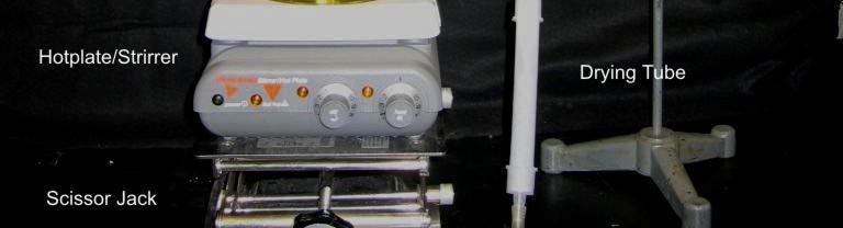


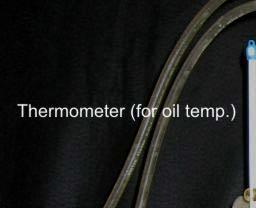
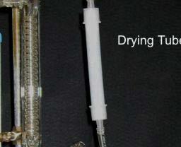


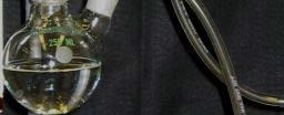
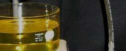
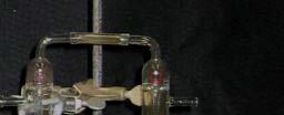
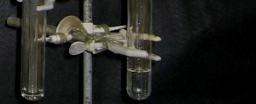


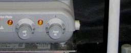
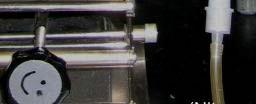

94 Figure A.1. Reflux set up
PIEZOELECTRIC TECHNOLOGY PRIMER
 PIEZOELECTRIC TECHNOLOGY PRIMER James R. Phillips Sr. Member of Technical Staff CTS Wireless Components 4800 Alameda Blvd. N.E. Albuquerque, New Mexico 87113 Piezoelectricity The piezoelectric effect is
Finite Element Analysis of Piezoelectric Cantilever
 Finite Element Analysis of Piezoelectric Cantilever Nitin N More Department of Mechanical Engineering K.L.E S College of Engineering and Technology, Belgaum, Karnataka, India. Abstract- Energy (or power)
Foundations of MEMS. Chang Liu. McCormick School of Engineering and Applied Science Northwestern University. International Edition Contributions by
 Foundations of MEMS Second Edition Chang Liu McCormick School of Engineering and Applied Science Northwestern University International Edition Contributions by Vaishali B. Mungurwadi B. V. Bhoomaraddi
Transduction Based on Changes in the Energy Stored in an Electrical Field
 Lecture 7-1 Transduction Based on Changes in the Energy Stored in an Electrical Field - Electrostriction The electrostrictive effect is a quadratic dependence of strain or stress on the polarization P
Mechanical characterization of single crystal BaTiO 3 film and insitu. XRD observation of microstructure change due to
 76 Chapter 4 Mechanical characterization of single crystal BaTiO 3 film and insitu XRD observation of microstructure change due to mechanical loading 4.1 Introduction Ferroelectric materials have many
Fabrication and performance of d 33 -mode lead-zirconate-titanate (PZT) MEMS accelerometers
 MEMS accelerometers") Fabrication and performance of d 33 -mode lead-zirconate-titanate (PZT) MEMS accelerometers H. G. Yu, R. Wolf*,K. Deng +,L.Zou +, S. Tadigadapa and S. Trolier-McKinstry* Department of Electrical Engineering,
Fabrication and performance of d 33 -mode lead-zirconate-titanate (PZT) MEMS accelerometers H. G. Yu, R. Wolf*,K. Deng +,L.Zou +, S. Tadigadapa and S. Trolier-McKinstry* Department of Electrical Engineering,
Outline. 4 Mechanical Sensors Introduction General Mechanical properties Piezoresistivity Piezoresistive Sensors Capacitive sensors Applications
 Sensor devices Outline 4 Mechanical Sensors Introduction General Mechanical properties Piezoresistivity Piezoresistive Sensors Capacitive sensors Applications Introduction Two Major classes of mechanical
Technical Report PZT-Silicon Cantilever Benders
 Radiant Technologies, Inc. 2021 Girard SE Albuquerque, NM 876 Tel: 505-842-8007 Fax: 505-842-0366 Technical Report PZT-Silicon Cantilever Benders Subject: Displacement Measurements of Silicon Cantilevers
SENSOR DEVICES MECHANICAL SENSORS
 SENSOR DEVICES MECHANICAL SENSORS OUTLINE 4 Mechanical Sensors Introduction General mechanical properties Piezoresistivity Piezoresistive sensors Capacitive sensors Applications INTRODUCTION MECHANICAL
Piezo materials. Actuators Sensors Generators Transducers. Piezoelectric materials may be used to produce e.g.: Piezo materials Ver1404
 Noliac Group develops and manufactures piezoelectric materials based on modified lead zirconate titanate (PZT) of high quality and tailored for custom specifications. Piezoelectric materials may be used
Thin Film Bi-based Perovskites for High Energy Density Capacitor Applications
 ..SKELETON.. Thin Film Bi-based Perovskites for High Energy Density Capacitor Applications Colin Shear Advisor: Dr. Brady Gibbons 2010 Table of Contents Chapter 1 Introduction... 1 1.1 Motivation and Objective...
COURSE OUTLINE. Introduction Signals and Noise Filtering Sensors: Piezoelectric Force Sensors. Sensors, Signals and Noise 1
 Sensors, Signals and Noise 1 COURSE OUTLINE Introduction Signals and Noise Filtering Sensors: Piezoelectric Force Sensors Piezoelectric Force Sensors 2 Piezoelectric Effect and Materials Piezoelectric
INTRODUCTION TO PIEZO TRANSDUCERS
 PIEZO SYSTEMS, INC. 65 Tower Office Park Woburn, MA 01801 USA Tel: 781 933 4850 Fax: 781 933 4743 email: sales@piezo.com Find Search for a product or category HOME PRODUCTS CUSTOM OEM CATALOG TECHNICAL
Piezoelectric Resonators ME 2082
 Piezoelectric Resonators ME 2082 Introduction K T : relative dielectric constant of the material ε o : relative permittivity of free space (8.854*10-12 F/m) h: distance between electrodes (m - material
Bending Load & Calibration Module
 Bending Load & Calibration Module Objectives After completing this module, students shall be able to: 1) Conduct laboratory work to validate beam bending stress equations. 2) Develop an understanding of
7.Piezoelectric, Accelerometer and Laser Sensors
 7.Piezoelectric, Accelerometer and Laser Sensors 7.1 Piezoelectric sensors: (Silva p.253) Piezoelectric materials such as lead-zirconate-titanate (PZT) can generate electrical charge and potential difference
Institute for Electron Microscopy and Nanoanalysis Graz Centre for Electron Microscopy
 Institute for Electron Microscopy and Nanoanalysis Graz Centre for Electron Microscopy Micromechanics Ass.Prof. Priv.-Doz. DI Dr. Harald Plank a,b a Institute of Electron Microscopy and Nanoanalysis, Graz
Piezo Theory: Chapter 1 - Physics & Design
 Piezoelectric effect inverse piezoelectric effect The result of external forces to a piezoelectric material is positive and negative electrical charges at the surface of the material. If electrodes are
ME 515 Mechatronics. Overview of Computer based Control System
 ME 515 Mechatronics Introduction to Sensors I Asanga Ratnaweera Department of Faculty of Engineering University of Peradeniya Tel: 081239 (3627) Email: asangar@pdn.ac.lk Overview of Computer based Control
Piezoactuators. Jiří Tůma
 Piezoactuators Jiří Tůma 1 Domain Piezoelectric effect Direct piezoelectric effect discovered the brothers Pierre and Jacques Curie. They found that certain crystalline materials (ceramics) having the
Addition 1. Shear Stack Piezoelectric Elements and Shear Effect Basics
 120 Addition 1 Shear Stack Piezoelectric Elements and Shear Effect Basics Introduction The STM scanner built up in this work is a Besocke type scanner (see room temperature STM instrumental chapter). The
SUPPLEMENTARY NOTES Supplementary Note 1: Fabrication of Scanning Thermal Microscopy Probes
 SUPPLEMENTARY NOTES Supplementary Note 1: Fabrication of Scanning Thermal Microscopy Probes Fabrication of the scanning thermal microscopy (SThM) probes is summarized in Supplementary Fig. 1 and proceeds
Modelling of Different MEMS Pressure Sensors using COMSOL Multiphysics
 International Journal of Current Engineering and Technology E-ISSN 2277 4106, P-ISSN 2347 5161 2017 INPRESSCO, All Rights Reserved Available at http://inpressco.com/category/ijcet Research Article Modelling
Principles of Active Vibration Control: Piezoelectric materials
 Principles of Active Vibration Control: Piezoelectric materials Introduction: Piezoelectric materials are materials that produce a voltage when stress is applied. Since, this effect also applies in the
ENSC387: Introduction to Electromechanical Sensors and Actuators LAB 3: USING STRAIN GAUGES TO FIND POISSON S RATIO AND YOUNG S MODULUS
 ENSC387: Introduction to Electromechanical Sensors and Actuators LAB 3: USING STRAIN GAUGES TO FIND POISSON S RATIO AND YOUNG S MODULUS 1 Introduction... 3 2 Objective... 3 3 Supplies... 3 4 Theory...
PERFORMANCE OF HYDROTHERMAL PZT FILM ON HIGH INTENSITY OPERATION
 PERFORMANCE OF HYDROTHERMAL PZT FILM ON HIGH INTENSITY OPERATION Minoru Kuribayashi Kurosawa*, Hidehiko Yasui**, Takefumi Kanda** and Toshiro Higuchi** *Tokyo Institute of Technology, Dept. of Advanced
440. Simulation and implementation of a piezoelectric sensor for harmonic in-situ strain monitoring
 440. Simulation and implementation of a piezoelectric sensor for harmonic in-situ strain monitoring 0. Incandela a, L. Goujon b, C. Barthod c University of Savoie, BP 80439 Annecy-le-Vieux CEDEX, France
Characterization of MEMS Devices
 MEMS: Characterization Characterization of MEMS Devices Prasanna S. Gandhi Assistant Professor, Department of Mechanical Engineering, Indian Institute of Technology, Bombay, Recap Fabrication of MEMS Conventional
SENSORS and TRANSDUCERS
 SENSORS and TRANSDUCERS Tadeusz Stepinski, Signaler och system The Mechanical Energy Domain Physics Surface acoustic waves Silicon microresonators Variable resistance sensors Piezoelectric sensors Capacitive
Instrumentation and Operation
 Instrumentation and Operation 1 STM Instrumentation COMPONENTS sharp metal tip scanning system and control electronics feedback electronics (keeps tunneling current constant) image processing system data
Sensors and Transducers. mywbut.com
 Sensors and Transducers 1 Objectives At the end of this chapter, the students should be able to: describe the principle of operation of various sensors and transducers; namely.. Resistive Position Transducers.
7. CONCLUSIONS & SCOPE
 7. CONCLUSIONS & SCOPE ENERGY harvesting is a critical technology for the expansion of self-governing, self-powered electronic devices. As the energy requirements of low-power electronics reduction, the
Laser Interferometric Displacement Measurements of Multi-Layer Actuators and PZT Ceramics
 Ferroelectrics, 320:161 169, 2005 Copyright Taylor & Francis Inc. ISSN: 0015-0193 print / 1563-5112 online DOI: 10.1080/00150190590967026 Laser Interferometric Displacement Measurements of Multi-Layer
User s Manual. STUDY OF DIELECTRIC CONSTANT Model: DEC-01
 User s Manual STUDY OF DIELECTRIC CONSTANT Model: DEC-01 Manufactured by.. Scientific Equipment & Services 358/1, New Adarsh Nagar, Roorkee - 247 667, UA, INDIA Ph.: +91-1332-272852, 277118 Fax: +91-1332-274831
Piezoelectric Fabrics for Energy Harvesting F06-GT05
 Piezoelectric Fabrics for Energy Harvesting F06-GT05 Project Leader: Principal Investigators: François M. Guillot, Georgia Institute of Technology, ME (francois.guillot@me.gatech.edu) Haskell W. Beckham,
MEMS Tuning-Fork Gyroscope Mid-Term Report Amanda Bristow Travis Barton Stephen Nary
 MEMS Tuning-Fork Gyroscope Mid-Term Report Amanda Bristow Travis Barton Stephen Nary Abstract MEMS based gyroscopes have gained in popularity for use as rotation rate sensors in commercial products like
The electric field induced strain behavior of single. PZT piezoelectric ceramic fiber
 The electric field induced strain behavior of single PZT piezoelectric ceramic fiber Xiong Yang a, Jing Zhou a,*, Sen Zhang a, Jie Shen b, Jing Tian a, Wen Chen a, Qi Zhang ac a State Key Laboratory of
CHAPTER 4 DESIGN AND ANALYSIS OF CANTILEVER BEAM ELECTROSTATIC ACTUATORS
 61 CHAPTER 4 DESIGN AND ANALYSIS OF CANTILEVER BEAM ELECTROSTATIC ACTUATORS 4.1 INTRODUCTION The analysis of cantilever beams of small dimensions taking into the effect of fringing fields is studied and
An Accurate Model for Pull-in Voltage of Circular Diaphragm Capacitive Micromachined Ultrasonic Transducers (CMUT)
") An Accurate Model for Pull-in Voltage of Circular Diaphragm Capacitive Micromachined Ultrasonic Transducers (CMUT) Mosaddequr Rahman, Sazzadur Chowdhury Department of Electrical and Computer Engineering
An Accurate Model for Pull-in Voltage of Circular Diaphragm Capacitive Micromachined Ultrasonic Transducers (CMUT) Mosaddequr Rahman, Sazzadur Chowdhury Department of Electrical and Computer Engineering
Technology Brief 9: Capacitive Sensors
 218 TEHNOLOGY BRIEF 9: APAITIVE SENSORS Technology Brief 9: apacitive Sensors To sense is to respond to a stimulus. (See Tech Brief 7 on resistive sensors.) A capacitor can function as a sensor if the
Integrating MEMS Electro-Static Driven Micro-Probe and Laser Doppler Vibrometer for Non-Contact Vibration Mode SPM System Design
 Tamkang Journal of Science and Engineering, Vol. 12, No. 4, pp. 399 407 (2009) 399 Integrating MEMS Electro-Static Driven Micro-Probe and Laser Doppler Vibrometer for Non-Contact Vibration Mode SPM System
DEPOSITION OF THIN TiO 2 FILMS BY DC MAGNETRON SPUTTERING METHOD
 Chapter 4 DEPOSITION OF THIN TiO 2 FILMS BY DC MAGNETRON SPUTTERING METHOD 4.1 INTRODUCTION Sputter deposition process is another old technique being used in modern semiconductor industries. Sputtering
Single-phase driven ultrasonic motor using two orthogonal bending modes of sandwiching. piezo-ceramic plates
 Single-phase driven ultrasonic motor using two orthogonal bending modes of sandwiching piezo-ceramic plates Yuting Ma 1,2, Minkyu Choi 2 and Kenji Uchino 2 1 CAS Key Lab of Bio-Medical Diagnostics, Suzhou
EE C247B / ME C218 INTRODUCTION TO MEMS DESIGN SPRING 2016 C. NGUYEN PROBLEM SET #4
 Issued: Wednesday, March 4, 2016 PROBLEM SET #4 Due: Monday, March 14, 2016, 8:00 a.m. in the EE C247B homework box near 125 Cory. 1. This problem considers bending of a simple cantilever and several methods
I. INTRODUCTION II. SAMPLE PREPARATION JOURNAL OF APPLIED PHYSICS VOLUME 92, NUMBER 5 1 SEPTEMBER
 JOURNAL OF APPLIED PHYSICS VOLUME 92, NUMBER 5 1 SEPTEMBER 2002 Longitudinal and transverse piezoelectric coefficients of lead zirconate titanateõvinylidene fluoride-trifluoroethylene composites with different
5. Building Blocks I: Ferroelectric inorganic micro- and nano(shell) tubes
 tubes") 5. Building Blocks I: Ferroelectric inorganic micro- and nano(shell) tubes 5.1 New candidates for nanoelectronics: ferroelectric nanotubes In this chapter, one of the core elements for a complex building
5. Building Blocks I: Ferroelectric inorganic micro- and nano(shell) tubes 5.1 New candidates for nanoelectronics: ferroelectric nanotubes In this chapter, one of the core elements for a complex building
2.76/2.760 Multiscale Systems Design & Manufacturing
 2.76/2.760 Multiscale Systems Design & Manufacturing Fall 2004 MOEMS Devices for Optical communications system Switches and micromirror for Add/drops Diagrams removed for copyright reasons. MOEMS MEMS
STRAIN GAUGES YEDITEPE UNIVERSITY DEPARTMENT OF MECHANICAL ENGINEERING
 STRAIN GAUGES YEDITEPE UNIVERSITY DEPARTMENT OF MECHANICAL ENGINEERING 1 YEDITEPE UNIVERSITY ENGINEERING FACULTY MECHANICAL ENGINEERING LABORATORY 1. Objective: Strain Gauges Know how the change in resistance
Piezoelectric Vibration Energy Harvesting. Characteristics of Barium Titanate Laminates
 Advances in Theoretical and Applied Mechanics, Vol. 9, 2016, no. 1, 43-54 HIKARI Ltd, www.m-hikari.com http://dx.doi.org/10.12988/atam.2016.634 Piezoelectric Vibration Energy Harvesting Characteristics
EE C247B / ME C218 INTRODUCTION TO MEMS DESIGN SPRING 2014 C. Nguyen PROBLEM SET #4
 Issued: Wednesday, Mar. 5, 2014 PROBLEM SET #4 Due (at 9 a.m.): Tuesday Mar. 18, 2014, in the EE C247B HW box near 125 Cory. 1. Suppose you would like to fabricate the suspended cross beam structure below
MECHANICS LAB AM 317 EXP 3 BENDING STRESS IN A BEAM
 MECHANICS LAB AM 37 EXP 3 BENDING STRESS IN A BEAM I. OBJECTIVES I. To compare the experimentally determined stresses in a beam with those predicted from the simple beam theory (a.k.a. Euler-Bernoull beam
INSTRUCTIONAL MANUAL. CURIE TEMPERATURE MEASUREMENT (For Ferroelectric Materials) Applied Science Department NITTTR, Sector-26, Chandigarh
 Applied Science Department NITTTR, Sector-26, Chandigarh") INSTRUTIONAL MANUAL URIE TEMPERATURE MEASUREMENT (For Ferroelectric Materials) Applied Science Department NITTTR, Sector-26, handigarh urie Temperature Measurement OBJETIE: Measurement of urie Temperature
INSTRUTIONAL MANUAL URIE TEMPERATURE MEASUREMENT (For Ferroelectric Materials) Applied Science Department NITTTR, Sector-26, handigarh urie Temperature Measurement OBJETIE: Measurement of urie Temperature
December 1999 FINAL TECHNICAL REPORT 1 Mar Mar 98
 REPORT DOCUMENTATION PAGE AFRL-SR- BL_TR " Public reporting burden for this collection of information is estimated to average 1 hour per response, including the time for reviewing instruct the collection
Y. C. Lee. Micro-Scale Engineering I Microelectromechanical Systems (MEMS)
") Micro-Scale Engineering I Microelectromechanical Systems (MEMS) Y. C. Lee Department of Mechanical Engineering University of Colorado Boulder, CO 80309-0427 leeyc@colorado.edu January 15, 2014 1 Contents
Micro-Scale Engineering I Microelectromechanical Systems (MEMS) Y. C. Lee Department of Mechanical Engineering University of Colorado Boulder, CO 80309-0427 leeyc@colorado.edu January 15, 2014 1 Contents
Magneto-Mechanical Modeling and Simulation of MEMS Sensors Based on Electroactive Polymers
 Magneto-Mechanical Modeling and Simulation of MEMS Sensors Based on Electroactive Polymers F.J.O. RODRIGUES, L.M. GONÇALVES, J.H. CORREIA, P.M. MENDES University of Minho, Dept. Industrial Electronics,
MODELING OF T-SHAPED MICROCANTILEVER RESONATORS. Margarita Narducci, Eduard Figueras, Isabel Gràcia, Luis Fonseca, Joaquin Santander, Carles Cané
 Stresa, Italy, 5-7 April 007 MODELING OF T-SHAPED MICROCANTILEVER RESONATORS Margarita Narducci, Eduard Figueras, Isabel Gràcia, Luis Fonseca, Joaquin Santander, Carles Centro Nacional de Microelectrónica
Highly piezoelectric, thermal stable ferroelectrets from cyclic olefin copolymer. Yan Li, Hui Wang, Changchun Zeng ANTEC 2015, Orlando
 Highly piezoelectric, thermal stable ferroelectrets from cyclic olefin copolymer Yan Li, Hui Wang, Changchun Zeng ANTEC 2015, Orlando Content 1. Introduction 2. COC ferroelectret 3. Hybrid COC-PDMS ferroelectret
Elasticity: Term Paper. Danielle Harper. University of Central Florida
 Elasticity: Term Paper Danielle Harper University of Central Florida I. Abstract This research was conducted in order to experimentally test certain components of the theory of elasticity. The theory was
Thermo-Mechanical Analysis of a Multi-Layer MEMS Membrane
 Thermo-Mechanical Analysis of a Multi-Layer MEMS Membrane Heiko Fettig, PhD James Wylde, PhD Nortel Networks - Optical Components Ottawa ON K2H 8E9 Canada Abstract This paper examines the modelling of
b. The displacement of the mass due to a constant acceleration a is x=
 EE147/247A Final, Fall 2013 Page 1 /35 2 /55 NO CALCULATORS, CELL PHONES, or other electronics allowed. Show your work, and put final answers in the boxes provided. Use proper units in all answers. 1.
Contactless Excitation of MEMS Resonant Sensors by Electromagnetic Driving
 Presented at the COMSOL Conference 2009 Milan University of Brescia Department of Electronics for Automation Contactless Excitation of MEMS Resonant Sensors by Electromagnetic Driving Marco Baù, VF V.
CHAPTER 5 FIXED GUIDED BEAM ANALYSIS
 77 CHAPTER 5 FIXED GUIDED BEAM ANALYSIS 5.1 INTRODUCTION Fixed guided clamped and cantilever beams have been designed and analyzed using ANSYS and their performance were calculated. Maximum deflection
Experiment Five (5) Principal of Stress and Strain
 Principal of Stress and Strain") Experiment Five (5) Principal of Stress and Strain Introduction Objective: To determine principal stresses and strains in a beam made of aluminum and loaded as a cantilever, and compare them with theoretical
Experiment Five (5) Principal of Stress and Strain Introduction Objective: To determine principal stresses and strains in a beam made of aluminum and loaded as a cantilever, and compare them with theoretical
Piezoelectric Actuator for Micro Robot Used in Nanosatellite
 Piezoelectric Actuator for Micro Robot Used in Nanosatellite R Bansevicius, S Navickaite, V Jurenas and A Bubulis PIEZOELECTRIC ACTUATOR FOR MICRO ROBOT USED IN NANOSATELLITE. R Bansevicius 1, S Navickaite,
Strain Sensor Design and Fabrication in Instrumented Suspensions
 Strain Sensor Design and Fabrication in Instrumented Suspensions Stanley Kon, Roberto Horowitz Department of Mechanical Engineering University of California at Berkeley December 31, 2004 Abstract Sub-millimeter
3rd International Symposium on Instrumentation Science and Technology
 Measurement of Longitudinal Piezoelectric Coefficients (d 33 of Pb(Zr 0.50,Ti 0.50 O 3 Thin Films with Atomic Force Microscopy LIU Meng-wei a, DONG Wei-jie b, TONG Jian-hua a, WANG Jing b, CUI Yan a, CUI
Creation of DIPOLE (two poles) (distortion of crystal structure by the small displacement of the ion in direction of electric field)
 (distortion of crystal structure by the small displacement of the ion in direction of electric field)") Dielectricity Dielectric materials: Materials which is generally insulators. Under applied electric field, there is a tiny movement of charge inside the material. Electric field Creation of DIPOLE (two
Dielectricity Dielectric materials: Materials which is generally insulators. Under applied electric field, there is a tiny movement of charge inside the material. Electric field Creation of DIPOLE (two
MEMS tunable gratings with analog actuation
 Information Sciences 149 (2003) 31 40 www.elsevier.com/locate/ins MEMS tunable gratings with analog actuation Wei-Chuan Shih *, Chee Wei Wong, Yong Bae Jeon, Sang-Gook Kim, George Barbastathis Department
Epitaxial piezoelectric heterostructures for ultrasound micro-transducers
 15 th Korea-U.S. Forum on Nanotechnology Epitaxial piezoelectric heterostructures for ultrasound micro-transducers Seung-Hyub Baek Center for Electronic Materials Korea Institute of Science and Technology
Wireless Sensor Networks. Picocube
 Wireless Sensor Networks Low Power Radio Power Storage Sensor Renewable Power Picocube Supply Vibrational Energy Scavenging Nathan Emley DRETD TAC Meeting February 19, 2008 Vibrational Scavenger Team:
Depolarization of a piezoelectric film under an alternating current field
 JOURNAL OF APPLIED PHYSICS 101, 054108 2007 Depolarization of a piezoelectric film under an alternating current field K. W. Kwok, a M. K. Cheung, H. L. W. Chan, and C. L. Choy Department of Applied Physics
MEMS Report for Lab #3. Use of Strain Gages to Determine the Strain in Cantilever Beams
 MEMS 1041 Report for Lab #3 Use of Strain Gages to Determine the Strain in Cantilever Beams Date: February 9, 2016 Lab Instructor: Robert Carey Submitted by: Derek Nichols Objective: The objective of this
Introduction to Microeletromechanical Systems (MEMS) Lecture 9 Topics. MEMS Overview
 Lecture 9 Topics. MEMS Overview") Introduction to Microeletromechanical Systems (MEMS) Lecture 9 Topics MicroOptoElectroMechanical Systems (MOEMS) Grating Light Valves Corner Cube Reflector (CCR) MEMS Light Modulator Optical Switch Micromirrors
Introduction to Microeletromechanical Systems (MEMS) Lecture 9 Topics MicroOptoElectroMechanical Systems (MOEMS) Grating Light Valves Corner Cube Reflector (CCR) MEMS Light Modulator Optical Switch Micromirrors
Sensor Principles and Microsensors Part 1
 Introduction to BioMEMS & Medical Microdevices Sensor Principles and Microsensors Part 1 Companion lecture to the textbook: Fundamentals of BioMEMS and Medical Microdevices, by Prof., http://saliterman.umn.edu/
Lecture 20. Measuring Pressure and Temperature (Chapter 9) Measuring Pressure Measuring Temperature MECH 373. Instrumentation and Measurements
 Measuring Pressure Measuring Temperature MECH 373. Instrumentation and Measurements") MECH 373 Instrumentation and Measurements Lecture 20 Measuring Pressure and Temperature (Chapter 9) Measuring Pressure Measuring Temperature 1 Measuring Acceleration and Vibration Accelerometers using
MECH 373 Instrumentation and Measurements Lecture 20 Measuring Pressure and Temperature (Chapter 9) Measuring Pressure Measuring Temperature 1 Measuring Acceleration and Vibration Accelerometers using
Piezoelectric Materials and Devices
 Piezoelectric Materials and Devices Applications in Engineering and Medical Sciences M. S. VIJAYA CRC Press Taylor & Francis Croup Boca Raton London NewYork CRC Press is an imprint of the Taylor & Francis
CAPACITIVE MICRO PRESSURE SENSORS WITH UNDERNEATH READOUT CIRCUIT USING A STANDARD CMOS PROCESS
 Journal of the Chinese Institute of Engineers, Vol. 26, No. 2, pp. 237-241 (2003) 237 Short Paper CAPACITIVE MICRO PRESSURE SENSORS WITH UNDERNEATH READOUT CIRCUIT USING A STANDARD CMOS PROCESS Ching-Liang
Basic Laboratory. Materials Science and Engineering. Atomic Force Microscopy (AFM)
") Basic Laboratory Materials Science and Engineering Atomic Force Microscopy (AFM) M108 Stand: 20.10.2015 Aim: Presentation of an application of the AFM for studying surface morphology. Inhalt 1.Introduction...
Basic Laboratory Materials Science and Engineering Atomic Force Microscopy (AFM) M108 Stand: 20.10.2015 Aim: Presentation of an application of the AFM for studying surface morphology. Inhalt 1.Introduction...
Supporting Information for: Flexible Energy Conversion
 Supporting Inormation or: Piezoelectric Nanoribbons Printed onto Rubber or Flexible Energy Conversion Yi Qi, Noah T. Jaeris, Kenneth Lyons, Jr., Christine M. Lee, Habib Ahmad, Michael C. McAlpine *, Department
Validation of High Displacement Piezoelectric Actuator Finite Element Models
 Validation of High Displacement Piezoelectric Actuator Finite Element Models Barmac Taleghani * Army Research Laboratory Vehicle Technology Directorate NASA Langley Research Center Hampton, VA ABSTRACT
Lecture 150 Basic IC Processes (10/10/01) Page ECE Analog Integrated Circuits and Systems P.E. Allen
 Page ECE Analog Integrated Circuits and Systems P.E. Allen") Lecture 150 Basic IC Processes (10/10/01) Page 1501 LECTURE 150 BASIC IC PROCESSES (READING: TextSec. 2.2) INTRODUCTION Objective The objective of this presentation is: 1.) Introduce the fabrication of
Lecture 150 Basic IC Processes (10/10/01) Page 1501 LECTURE 150 BASIC IC PROCESSES (READING: TextSec. 2.2) INTRODUCTION Objective The objective of this presentation is: 1.) Introduce the fabrication of
Introduction. Procedure. In this experiment, you'll use the interferometer to EQUIPMENT NEEDED: Lens 18mm FL. Component holder.
 12-7137A Precision Interferometer Experiment 1: Introduction to Interferometry EQUIPMENT NEEDED: Basic Interferometer (OS-9255A) Laser (OS-9171) Laser Alignment Bench (OS-9172) Interferometer Accessories
Strain, Force, and Pressure
 10-1 10-1 Strain, Force, and Pressure Force is that which results in acceleration (when forces don t cancel). Strain is the change in shape of an object...... usually due to some force. (Force is usually
Effects of niobium doping on the piezoelectric properties of sol gel-derived lead zirconate titanate films
 JOURNAL OF APPLIED PHYSICS VOLUME 95, NUMBER 3 1 FEBRUARY 2004 Effects of niobium doping on the piezoelectric properties of sol gel-derived lead zirconate titanate films K. W. Kwok, a) R. C. W. Tsang,
Biosensors and Instrumentation: Tutorial 2
 Biosensors and Instrumentation: Tutorial 2. One of the most straightforward methods of monitoring temperature is to use the thermal variation of a resistor... Suggest a possible problem with the use of
Simulation based Analysis of Capacitive Pressure Sensor with COMSOL Multiphysics
 Simulation based Analysis of Capacitive Pressure Sensor with COMSOL Multiphysics Nisheka Anadkat MTech- VLSI Design, Hindustan University, Chennai, India Dr. M J S Rangachar Dean Electrical Sciences, Hindustan
Etching: Basic Terminology
 Lecture 7 Etching Etching: Basic Terminology Introduction : Etching of thin films and sometimes the silicon substrate are very common process steps. Usually selectivity, and directionality are the first
Strain Measurement. Prof. Yu Qiao. Department of Structural Engineering, UCSD. Strain Measurement
 Strain Measurement Prof. Yu Qiao Department of Structural Engineering, UCSD Strain Measurement The design of load-carrying components for machines and structures requires information about the distribution
ENERGY LOSS CHARACTERIZATION OF THE P3 MEMS HEAT ENGINE. KIRSTEN ELIZABETH McNEIL
 ENERGY LOSS CHARACTERIZATION OF THE P3 MEMS HEAT ENGINE By KIRSTEN ELIZABETH McNEIL A thesis submitted in partial fulfillment of the requirements for the degree of MASTER OF SCIENCE IN MECHANICAL ENGINEERING
Laboratory 7 Measurement on Strain & Force. Department of Mechanical and Aerospace Engineering University of California, San Diego MAE170
 Laboratory 7 Measurement on Strain & Force Department of Mechanical and Aerospace Engineering University of California, San Diego MAE170 Megan Ong Diana Wu Wong B01 Tuesday 11am May 17 th, 2015 Abstract:
MAS.836 PROBLEM SET THREE
 MAS.836 PROBLEM SET THREE FSR, Strain Gauge, and Piezo Circuits: The purpose of this problem set is to familiarize yourself with the most common forms of pressure and force measurement. The circuits you
Mechatronics II Laboratory EXPERIMENT #1 MOTOR CHARACTERISTICS FORCE/TORQUE SENSORS AND DYNAMOMETER PART 1
 Mechatronics II Laboratory EXPEIMENT #1 MOTO CHAACTEISTICS FOCE/TOQUE SENSOS AND DYNAMOMETE PAT 1 Force Sensors Force and torque are not measured directly. Typically, the deformation or strain of some
Part 2. Sensor and Transducer Instrument Selection Criteria (3 Hour)
") Part 2 Sensor and Transducer Instrument Selection Criteria (3 Hour) At the end of this chapter, you should be able to: Describe the definition of sensor and transducer Determine the specification of control
Part 2 Sensor and Transducer Instrument Selection Criteria (3 Hour) At the end of this chapter, you should be able to: Describe the definition of sensor and transducer Determine the specification of control
Piezoelectric Multilayer Beam Bending Actuators
 R.G. Bailas Piezoelectric Multilayer Beam Bending Actuators Static and Dynamic Behavior and Aspects of Sensor Integration With 143 Figures and 17 Tables Sprin ger List of Symbols XV Part I Focus of the
Finite Element Modeling of Ultrasonic Transducers for Polymer Characterization
 Excerpt from the Proceedings of the COMSOL Conference 2009 Milan Finite Element Modeling of Ultrasonic Transducers for Polymer Characterization Serena De Paolis *, Francesca Lionetto and Alfonso Maffezzoli
Active elastomer components based on dielectric elastomers
 Gummi Fasern Kunststoffe, 68, No. 6, 2015, pp. 412 415 Active elastomer components based on dielectric elastomers W. Kaal and S. Herold Fraunhofer Institute for Structural Durability and System Reliability
1. Narrative Overview Questions
 Homework 4 Due Nov. 16, 010 Required Reading: Text and Lecture Slides on Downloadable from Course WEB site: http://courses.washington.edu/overney/nme498.html 1. Narrative Overview Questions Question 1
RTAC104 AFM References in Package
 Radiant Technologies, Inc. 2835D Pan American Freeway NE Albuquerque, NM 87107 Tel: 505-842-8007 Fax: 505-842-0366 e-mail: radiant@ferrodevices.com www.ferrodevices.com RTAC104 AFM References in Package
MENG 302L Lab 6: Stress Concentration
 Introduction 1 : The purpose of this experiment is to demonstrate the existence of stress and strain concentration in the vicinity of a geometric discontinuity in a cantilever beam, and to obtain an approximate
Modeling, Simulation and Optimization of the Mechanical Response of Micromechanical Silicon Cantilever: Application to Piezoresistive Force Sensor
 Available online at www.sciencedirect.com ScienceDirect Physics Procedia 55 (2014 ) 348 355 Eight International Conference on Material Sciences (CSM8-ISM5) Modeling, Simulation and Optimization of the