Interface ABSTRACT. Atomically engineered oxide multilayers and superlattices display unique properties
|
|
|
- Sabina Booker
- 5 years ago
- Views:
Transcription
1 Oxygen-Induced Surface Reconstruction of SrRuO 3 and Its Effect on the BaTiO 3 Interface Junsoo Shin,,,* Albina Y. Borisevich, Vincent Meunier, Jing Zhou, E. Ward Plummer, Sergei V. Kalinin, and Arthur P. Baddorf,,* Department of Physics and Astronomy, The University of Tennessee, Knoxville, TN 37996, Materials Sciences and Technology Division, Oak Ridge National Laboratory, Oak Ridge, TN 37831, Computer Science and Mathematics Division, Oak Ridge National Laboratory, Oak Ridge, TN 37831, Department of Chemistry, University of Wyoming, Laramie, WY 82071, Department of Physics and Astronomy, Louisiana State University, Baton Rouge, LA, 70803, Center for Nanophase Materials Sciences, Oak Ridge National Laboratory, Oak Ridge, TN ABSTRACT Atomically engineered oxide multilayers and superlattices display unique properties responsive to the electronic and atomic structures of the interfaces. We have followed the growth of ferroelectric BaTiO 3 on SrRuO 3 electrode with in situ atomic scale analysis of the surface structure at each stage. An oxygen-induced surface reconstruction of SrRuO 3 leads to formation of SrO rows spaced at twice the bulk periodicity. This reconstruction modifies the structure of the first BaTiO 3 layers grown subsequently, including intermixing observed with cross-section spectroscopy. These observations reveal that this common oxide interface is much more interesting than previously reported, and provide a paradigm for oxygen engineering of oxide structure at an interface. * Address correspondence to jshin@ornl.gov, baddorfap@ornl.gov. 1
2 Advances in atomically-controlled oxide growth have generated new classes of materials with unique physical properties highly sensitive to abrupt interfaces. 1 4 The extreme sensitivity of oxides to electron concentration is coupled to charge transfer, structure, and spin to produce spectacular behavior including interface mediated conduction, 3,5,6 superconductivity, 7 magnetism, 8 and phase transitions 9,10 in parent materials lacking these attributes. The response of oxides to structural instabilities or disorder is greater in twodimensional systems, seen in examples of Anderson localization, Peierls instability or charge density wave transitions. The central role of oxygen stoichiometry has been repeatedly shown in defining both structure and properties of oxide interfaces, and can be tuned as a means to control static and dynamic distributions of electrons and atoms for a new generation of functional materials with applications ranging from oxide sensors and electronics to energy capture and storage. Nevertheless, few atomic scale studies of interface structures exist for complex oxides, due to a need for multiple tools to probe subsurface features, the need for a highly controlled environment, 14,15 and the insulating nature of many oxides. We have studied the structural evolution of surfaces and interfaces during the layerby-layer growth of BaTiO 3 films on SrRuO 3. This pair combines the classic ferroelectric, BaTiO 3, and the most common conducting oxide, SrRuO 3, and has been the subject of a number of investigations. 11,16 By combining in situ measurements of in-plane surface structure, ex situ cross sectional microscopy and spectroscopy, and first principles simulations, we observed the atomic structure of SrRuO 3 surfaces and its impact on the interface and structure of several layers of BaTiO 3. Surprisingly, the SrRuO 3 surface, which has conventionally been considered flat based on observation of well-separated, single layer steps in ex situ atomic force microscopy (AFM), is reconstructed at atomic length scales. This 2
3 reconstruction increases the oxygen concentration and leads to both intermixing and structural change in BaTiO 3 at the interface. Clearly, AFM lacking atomic resolution cannot be relied upon to identify structural or stoichiometric deviations. In situ characterization of films must become the norm to identify the fundamental origins of behavior. SrRuO 3 and BaTiO 3 films were grown on (001) oriented SrTiO 3 substrates using pulsed laser deposition with protocols described in the Methods section. To study the interface structure between BaTiO 3 and SrRuO 3 films, 1, 2, 4 and 10 unit cell BaTiO 3 films were grown on SrRuO 3 /SrTiO 3. The detailed deposition conditions and the in situ electron diffraction experiments of BaTiO 3 /SrRuO 3 films on SrTiO 3 are reported elsewhere. 17 The growth quality and quantity of deposited material were confirmed using Reflection High Energy Electron Diffraction (RHEED). As shown in Figure 1A and Figure 1B, diffraction intensities oscillated as materials were deposited with each oscillation indicating one layer of film growth. For SrRuO 3, RHEED intensities oscillated several times but quickly reached a steady state, which has been shown to reflect a transition from layer-bylayer growth to step-flow growth with a SrO surface termination. 18 BaTiO 3 growth produced extended oscillations indicating good layer-by-layer growth and revealing the number of layers (one per oscillation) as they were grown. The flatness of these films was assured by removing several samples from vacuum for Atomic Force Microscopy (AFM). While exposure to atmosphere results in adsorption which could affect the surface structure, 14 ambient AFM images were useful as a comparison to many previous studies. Results shown in Figures 1C, D, and E, show these films were smooth with only single unit-cell steps and step densities similar to that of the TiO 2 -terminated SrTiO 3 substrates. 3
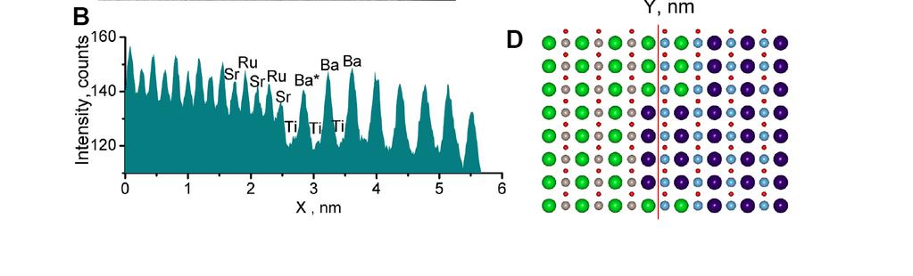
4 The expectation, then, was that the interface between SrRuO 3 and BaTiO 3 would be atomically flat. Buried interfaces are notoriously difficult to characterize on an atomic scale; scanning probes, or other surface methods, cannot access the region of interest. Here, we examined this interface with cross-sectional Scanning Transmission Electron Microscopy (STEM). In Z-contrast STEM imaging, the intensity of an atomic column in the image is roughly proportional to the square of its atomic number, providing contrast between the two materials. The interface between SrRuO 3 and BaTiO 3 is clearly seen in Figure 2A where TiO 2 planes take over from more intense RuO 2 planes. Image profiles help quantify the transition. The profile in Figure 2B corresponds to the box on the image in Figure 2A, i.e. it represents an average over 6 atomic rows parallel to the interface. A general intensity decrease from left to right in the image originates from the decreasing specimen thickness. The individual column intensities follow the composition, for example, the SrO termination of the SrRuO 3 is clearly observed. Interestingly, the first BaO column marked Ba* has a considerably reduced intensity relative to others. This suggests the depletion of Ba or presence of Sr in this column. If, however, we construct a profile from individual rows across the image and track the intensities of the SrO and BaO columns closest to the interface, it becomes clear that this compositional change is not uniform. In Figure 2C we plot the corresponding peak heights (obtained from Gaussian fits of the profiles) in the image in Figure 2A as a function of vertical coordinate (along the interface). The last SrO layer and the first BaO layer have variable profiles, implying changing compositions. It is important to discern that these layers are correlated in composition, i.e. the two layers nearest the interface can be both BaO, both SrO, or both mixed at about the same degree. The composition of these layers varies on a nanometer scale forming domains along the interface. The presence of mixed BaO/SrO 4
5 columns does not necessarily imply mixing on an atomic scale; because the observed compositional domains could have dimensions as small as 2 nm (see Figure 2C), there could be overlap in the beam direction (normal to the image plane) resulting in apparent mixing. The cumulative BaO/SrO ratio in these rows calculated over the entire image is very close to 1:1, suggesting that stoichiometry is preserved overall. The observed contrast pattern indicates that the interface has a complex structure, possibly similar to the schematic in Figure 2D, but not atomically smooth. These observations led us to examine the SrRuO 3 surface in more detail. Higher resolution, obtained with in situ scanning tunneling microscopy (STM) revealed a more complex picture of the SrRuO 3 surface. The images in Figure 3 were acquired at 1.4V and 40 pa. STM images, such as those shown in Figures 3A and B, resolve features the size of an individual unit cell (0.4 nm). These images show rows of atoms in the surface plane oriented along (110) and (1-10) crystallographic directions. These rows are interspersed with a number of missing atoms, creating a large fraction of defects in the ordering. Line analysis (Figure 3C) of the STM images show that the spacing along the rows is 0.6±0.05 nm and corrugation about 0.004±0.002 nm while the spacing between the rows (Figure 3D) is 1.2±0.05 nm with much larger corrugation of 0.10±0.01 nm. Along the rows, therefore, the spacing corresponds to a single unit cell ( 2 times the lattice constant of SrTiO 3, nm), while the spacing between rows is twice that value, i.e. every second substrate unit cell. It is clear that these rows and holes, unobserved with ex situ AFM, will provide a profound effect on the surface and interface properties and on subsequent growth mechanisms of materials such as BaTiO 3. 5
6 Low Energy Electron Diffraction (LEED) revealed the evolution of long-range ordered structures at several stages of the film growth. As this technique involves scattering of electrons with energies typically between 50 and 200 ev, a conducting substrate is needed to avoid charging which would mask the diffraction pattern. Patterns were obtained from SrRuO 3 and from thin films of BaTiO 3 on SrRuO 3. As shown in Figure 5B, the diffraction pattern from SrRuO 3 thin film surfaces had not only the square pattern expected from a bulkterminated film, but also an addition spot halfway between each bulk spot. This pattern showed the surface unit cell periodicity was doubled in both surface crystallographic directions, a periodicity known as p(2x2). This diffraction pattern is consistent with the rows observed in STM that were separated by twice the bulk lattice constant. However, the STM images revealed that the local periodicity is established by rows along either (100) or (010) directions, i.e. local domains of (2x1) and (1x2) symmetry that sum together to appear as a p(2x2) pattern. Analysis of the growth of SrRuO 3 on STO has shown that the surface is terminated by a SrO layer, with RuO 2 below. 18 Since Sr has a greater density of conducting electronic states than oxygen, Sr atoms most likely are imaged by STM. The images suggested therefore that Sr or a Sr oxide is responsible for the rows. The holes between rows (i.e. where rows are incomplete) are similar to those seen with STM on surfaces of layered Sr-Ru oxides, including Sr 2 RuO 4 and Sr 3 Ru 2 O 7, although these materials exhibit a c(2x2) symmetry, without extended rows. 19 This corrugated, imperfect surface can also help explain the unexpected surface reactivity of the surface when exposed to atmosphere. 14,20 To identify the rowed structure observed experimentally, we examined several structural candidates using first principles density functional theory (DFT). We initially 6
7 verified the effect of removing single SrO dimers from the SrRuO 3 surface; a dimer being charge neutral is more likely than a single atom to produce a stable structure. The observed vertical corrugation between rows in STM was 0.1 nm, not too different than the ~ 0.15 nm dip corresponding to the rigid removal of a pair from bulk SrRuO 3. However, the computed energy to remove a SrO dimer is prohibitively large, costing ~ 7 ev/pair. This large extraction energy can be understood since the process involves breaking covalent bonds with an accompanying energy penalty that is not counterbalanced by the creation of other bonds. We next investigated the energetics related to the removal and elevation of a SrO dimer onto the surface (i.e. the SrO pair is promoted from the surface layer over the surface), in such a way that part of the energy associated with the creation of the SrO vacancy is compensated by bond formation with top atoms. This could be expected to be an unstable configuration, and indeed, during the calculation most of the initial configurations relax back in to the cleaned, defect-free surface (Figure 4A). However, appropriate surface structures, for example the Sr and O geometry of Figure 4B, did support bonding creating a local energy minimum, i.e. a metastable configuration. In the observed (2x1)+(1x2) rows, isolated defects appear less stable than a row of defects. Computationally, we found that a row of SrO is more stable, by 0.32 ev/pair, and that the preferential ordering was along the (110), or equivalently (1-10), direction. The structure corresponding to complete rows of defects is shown in Figure 4B, and corresponds to a formation energy of ev/pair when compared to a defect-free surface. As expected the defect formation energy was significantly lowered when the SrO remains bound to the surface, rather than simply ejected from it. Nevertheless, the reduced number of Ru-O and Sr- O bonds still leaves the energy cost too high to explain the observations. 7
8 In the oxygen rich atmosphere required to approach stoichiometric growth of oxides such as SrRuO 3, molecular oxygen should be very reactive with displaced Sr as described above. We focused next our attention on O interactions with the rowed SrO structure, where SrO is promoted onto the surface. In Figure 4C, we present the minimum energy structures resulting from the interaction of O 2 with the system of Figure 4B. When a single O is added per displaced SrO, its stable position is directly above the underbonded Ru (small white sphere), close to the position of the displaced O in the pristine surface. More importantly, the system energy is considerably reduced by 4.76 ev/o, which is much larger that the corresponding 1.2 ev/o adsorption energy on a defect-free surface. In other words, the defect energy was reduced to 1.78 ev/sro. This formation energy, calculated at 0 K, is sufficiently low to suggest that SrO rows, displaced from the surface layer, together with excess oxygen, could produce the observed structure. The calculations continue to indicate that this structure should be metastable, which is consistent with STM measurements that will be discussed elsewhere. As 1-2 layers of BaTiO 3 were grown on SrRuO 3, the LEED pattern remained p(2x2) (Figure 5B), however the relative intensities of diffraction spots were altered from those observed from SrRuO 3 alone. This change in relative intensities indicates a change of structure, with two important implications. First, this pattern must represent the order of the BaTiO 3 film, and cannot arise solely from exposed remnants of SrRuO 3. Second, this shows that the SrRuO 3 reconstruction influences the structure of the BaTiO 3 at the interface, which does not share the symmetry of bulk BaTiO 3, but instead has a periodicity two times larger in the plane of the interface. 8
9 Growth of thicker BaTiO 3 reverts the pattern observed in LEED to the (1x1) symmetry of the bulk. As shown in Figure 5B, as few as 4 layers of BaTiO 3 produce at a (1x1) periodicity; the additional diffraction spots indicating a doubled unit cell are gone. STM images of Figure 5C and D show the local periodic atomic rows along either (100) or (010) direction whereas Figure 5E no longer reveal rows. The same periodicity and surface topography remain in films of 10 layers of BaTiO 3. The LEED technique is highly surface sensitive, owing to the short mean-free path of low energy electrons in matter. Consequently, while the surfaces of these films show no reconstruction, i.e. no deviation of the in-plane symmetry from the bulk, the p(2x2) structure could persist at the interface. A reconstructed interface would have a profound influence on our understanding and modeling of phenomena such as the recent studies showing well-defined interfaces with remanent polarization down to 3.5 nm, 21,22 interface closure domains, 23 and ferroelectric effects on electron tunneling 24 in ultrathin films. It is clear from these combined studies using STM, STEM, LEED, and DFT theory that the surfaces and interfaces of oxides as common as SrRuO 3 and BaTiO 3, each widely applied for their conductivity and ferroelectricity, respectively, can be more complex than previously assumed. The goal of an atomically abrupt interface in heteroepitaxy can be foiled by the intrinsic differences of terminated materials. In this example, conventional AFM imaging failed to identify a restructuring of the SrRuO 3 surface, where excess oxygen leads to rows of SrO along (100) or (010) crystallographic directions that double the unit cell periodicity. When buried under a BaTiO 3 film, these rows lead to an interface with mixed SrO and BaO composition and an in-plane doubling of the periodicity of the first few BaTiO 3 layers. This combined approach, including in situ characterization and modeling at an atomic 9
10 scale, presents a new archetype for identification of oxygen stoichiometry and interface structure required for control of functional properties, for example ferroelectricity and transport in thin films. METHODS A 15-nm-thick SrRuO 3 film was deposited on TiO 2 -terminated 25 SrTiO 3 (001) substrate by PLD with layer thickness and growth mode monitored by high-pressure RHEED in the growth chamber with a base pressure 1x10⁻⁸ Torr. Growth parameters of substrate temperature and oxygen pressure were 700 C and 100 mtorr with an average deposition flux of 0.05 unit cells/s. 26 A KrF excimer laser (λ = 248 nm) was used for growing films at a repetition rate of 5 Hz. After deposition, samples were kept in situ and annealed at 450 C for 90 min in 1 Torr O 2 after growth and then cooled down to room temperature. Subsequently, the pressure was lowered and the samples were transferred without exposure in air to the ultra high vacuum (2x10⁻¹⁰ Torr) STM and LEED chambers. Calculations for structural investigation were performed within DFT, using the Vienna ab initio simulation package (VASP). 27,28 The Kohn-Sham equations were solved using the projector augmented wave (PAW) approach 29,30 and a plane-wave basis with a 400 ev energy cutoff and the exchange-correlation functional was represented by the Local Density Approximation (LDA). 31 Spin polarized calculations were used throughout. The system was set-up as follows: first we relaxed a SrTiO 3 (STO) unit cell in bulk using a 12x12x12 Monkhorst-Pack Brillouin zone sampling, resulting to a crystal structure with a=b=0.546 nm and c=3.863 nm. We used a single 2x2 slab of STO along as support. The atoms in this slab were kept fixed during the course of all the simulations. Imposing the lattice constants of STO 10
11 in bulk, this results in a unit cell of x nm2 for the planar dimension. The system, called cleaned or defect-free surface hereafter, was obtained by adding and relaxing a 2x2 (001) slab of SrRuO 3 on top of the previously position STO, resulting in a 96 atom unit cell. We chose the c-axis of the working unit in such a way as to ensure a minimum of 0.7 nm of vacuum between periodic images. That unit cell was used as a starting point for all the calculations shown here. Note that we used a 4x4x1k-point grid for the slab calculations. ACKNOWLEDGMENTS Research was sponsored by the Division of Materials Science and Engineering (JS) and at the Center for Nanophase Materials Sciences (SVK and APB) by the Scientific User Facilities Division, at Oak Ridge National Laboratory, for the Office of Basic Energy Sciences, U. S. Department of Energy. This work was also partially supported by the Department of Energy Grant DE-SC (EWP). 11
12 REFERENCES 1. Junquera, J.; Ghosez, P. Critical Thickness for Ferroelectricity in Perovskite Ultrathin Films. Nature 2003, 422, Ahn, C. H.; Triscone, J.-M.; Mannhart, J. Electric Field Effect in Correlated Oxide Systems. Nature 2004, 424, Ohtomo, A.; Hwang, H.Y. A High-Mobility Electron Gas at the LaAlO 3 /SrTiO 3 Heterointerface. Nature 2004, 427, Nakagawa, N.; Hwang, H.Y.; Muller, D. Why Some Interfaces Cannot Be Sharp. Nature Materials 2006, 5, Maksymovych, P.; Jesse, S.; Yu, P.; Ramesh, R.; Baddorf, A. P.; Kalinin, S. V. Polarization Control of Electron Tunneling into Ferroelectric Surfaces. Science 2009, 324, Garcia, V.; Fusil, S.; Bouzehouane, K.; Enouz-Vedrenne, S.; Mathur, N. D.; Barthélémy, A.; and Bibes, M. Giant Tunnel Electroresistance for Non-Destructive Readout of Ferroelectric States. Nature 2009, 460, Reyren, N.; Thiel, S.; Caviglia, A.D.; Kourkoutis, L.F.; Hammert, G.; Richter, C.; Schneider, C.W.; Kopp, T.; Ruetschi, A.-S.; Jaccard, D.; et al. Superconducting Interfaces between Insulating Oxides. Science 2007, 317, Takahashi, K.S.; Kawasaki, M.; Tokura, Y. Interface Ferromagnetism in Oxide Superlattices of CaMnO 3 /CaRuO 3. Appl. Phys. Lett. 2001, 79, Hoppler, J.; Stahn, J.; Niedermayer, Ch.; Malik, V.K.; Bouyanfif, H.; Drew, A.J.; Rössle, M.; Buzdin, A.; Cristiani, G.; Habermeier, H.-U.; et al. Giant Superconductivity-Induced Modulation of the Frromagnetic Magnetization in a Cuprate-Manganite Superlattice. Nature Materials 2009, 8, Moore, R.G.; Zhang, J.; Nascimento, V.B.; Jin, R.; Jiandong Guo; Wang, G.T.; Fang, Z.; Mandrus, D.; Plummer, E.W. A Surface-Tailored, Purely Electronic, Mott Metal-to- Insulator Transition. Science 2007, 318, Diebold, U. Structure and Properties of TiO 2 Surfaces: A Brief Review. Appl. Phys. A, 2003, 5,
13 12. Kolpak, A. M.; Dongbo, Li; Rui, Shao; Rappe, A. M.; Bonnell, D. A. Evolution of the Structure and Thermodynamic Stability of the BaTiO 3 Surface. Phys. Rev. Lett. 2008, 101, Herranz, G.; Basletic, M.; Bibes, M.; Carretero, C.; Tafra, E.; Jacquet, E.; Bouzehouane, K.; Deranlot, C.; Hamzic, A.; Broto, J. M.; et al. High Mobility in LaAlO 3 /SrTiO 3 Heterostructures: Origin, Dimensionality, and Perspectives. Phys. Rev. Lett. 2007, 98, Shin, J.; Kalinin, S.V.; Lee, H.N.; Christen, H.M.; Moore, R.G.; Plummer, E.W.; Baddorf, A.P. Surface Stability of Epitaxial SrRuO 3 Films. Surf. Sci. 2005, 581, Shin, J; Nascimento, V.B.; Geneste, G.; Rundgren, J.; Plummer, E.W.; Dkhil, B.; Kalinin, S.V.; Baddorf, A.P. Atomistic Screening Mechanism of Ferroelectric Surfaces: An In Situ Study of the Polar Phase in Ultrathin BaTiO 3 Films Exposed to H 2 O. Nano Lett. 2009, Tagantsev, A.K.; Gerra, G.; Setter, N. Short-Range and Long-Range Contributions to the Size Effect in Metal-Ferroelectric-Metal Heterostructures. Phys. Rev. B 2008, 77, Shin, J.; Nascimento, V.B.; Borisevich, A.Y.; Plummer, E.W.; Kalinin, S.V.; Baddorf, A.P. Polar Distortion in Ultrathin BaTiO 3 Films Studied by In Situ LEED I-V. Phys. Rev. B 2008, 77, Rijnders, G.; Blank, D.H.A.; Choi, J.; Eom, C.-B. Enhanced Surface Diffusion through Termination Conversion during Epitaxial SrRuO 3 Growth. Appl. Phys. Lett. 2004, 84, Plummer, E.W.; Ismail; Matzdorf, R.; Melechko, A.V.; Zhang, J. The Next 25 Years of Surface Physics. Prog. Surf. Sci. 2001, 67, Shin, J.; Kalinin, S.V.; Lee, H.N.; Christen, H.M.; Moore, R.G.; Plummer, E.W.; Baddorf, A.P. Surface Stability of Epitaxial SrRuO 3 Thin Films in Vacuum. J. Mater. Res. 2004, 19, Petraru, A.; Kohlstedt, H.; Poppe, U.; Waser, R.; Solbach, A.; Klemradt, U.; Schubert, J.; Zander, W.; Pertsev, N.A. Wedgelike Ultrathin Epitaxial BaTiO 3 Films for Studies of Scaling Effects in Ferroelectrics. Appl. Phys. Lett., 2008, 93,
14 22. Kim, Y.S.; Jo, J.Y.; Kim, D.J.; Chang, Y.J.; Lee, J.H.; Noh, T.W.; Song, T.K.; Yoon, J.- G.; Chung, J.-S.; Baik, S.I.; et al. Ferroelectric Properties of SrRuO 3 /BaTiO 3 /SrRuO 3 Ultrathin Film Capacitors Free from Passive Layers. Appl. Phys. Lett., 2006, 88, Aguado-Puente, P.; Junquera, J. Ferromagneticlike Closure Domains in Ferroelectric Ultrathin Films: First-Principles Simulations. Phys. Rev. Lett., 2008, 100, Gruverman A.; Wu D.; Lu H.; Wang Y.; Jang H.W.; Folkman C.M.; Zhuravlev M. Ye; Felker D.; Rzchowski M.; Eom C.-B.; et al. Tunneling Electroresistance Effect in Ferroelectric Tunnel Junctions at the Nanoscale. Nano Lett. 2009, 9, Kawasaki, M.; Takahashi, K.; Maeda, T.; Tsuchiya, R.; Shinohara, M.; Ishiyama, O.; Yonezawa, T.; Yoshimoto, M.; Koinuma, H. Atomic Control of the SrTiO 3 Crystal Surface. Science 1994, 266, Shin, J.; Kalinin, S.V.; Borisevich, A.Y.; Plummer, E.W.; Baddorf, A.P. Layer-by-Layer and Pseudo-Two-Dimensional Growth Modes for Heteroepitaxial BaTiO3 Films by Exploiting Kinetic Limitations. Appl. Phys. Lett. 2007, 91, Kresse, G; Hafner, G. Ab Initio Molecular Dynamics for Liquid Metals. Phys. Rev. B. 1993, 47, Kresse, G.; Furthmuller, J. Efficient Iterative Schemes for Ab Initio Total-Energy Calculations using a Plane-Wave Basis Set. Phys. Rev. B 1996, 54, Kresse, G.; Joubert, D. From Ultrasoft Pseudopotentials to the Projector Augmented- Wave Method. Phys. Rev. B 1999, 59, Blochl P.E. Projector augmented-wave method. Phys. Rev. B 1994, 50, Ceperley, D.M.; Alder, B. J. Ground State of the Electron Gas by a Stochastic Method. Phys. Rev. Lett. 1980, 45,
15 Figure Captions Fig. 1. In situ RHEED oscillation during and RHEED pattern after (A) SrRuO 3 deposition and (B) 10 unit cells of BaTiO 3 deposition. Ex situ AFM topography of 3x3 μm 2 regions of (C) 15 nm thick SrRuO 3 thin film, (D) 2 unit cells thick BaTiO 3, and (E) 10 unit cells thick BaTiO 3 thin films on SrRuO 3 /SrTiO 3. Fig. 2. (A) High angle annular dark field STEM image of the BaTiO 3 /SrRuO 3 /SrTiO 3 film in cross-section; (B) intensity profile averaged over area in the blue box in (A), showing decreased intensity in the first Ba column denoted as Ba*, (C) Ba and Sr column intensities in the vicinity of the interface (color coding on right) as a function of vertical coordinate of the image (black Ba and green Sr correspond to the first columns near the interface), (D) interface structure suggested from STEM images, with ideal interface position indicated by red line (Sr green, Ru grey, O- red, Ba purple, Ti blue). Fig. 3. Scanning Tunneling Microscopy images of the thin film SrRuO 3 surface showing (A) rows and their long range periodicity, (B) a higher resolution scan with line profiles, (C) along the rows where the spacing is 0.6 nm, and (D) across the rows which are separated by 1.2 nm. The (2x1) unit cell (white rectangle) is indicated in (B). Fig. 4. SrRuO 3 models viewed from the top (upper panels) and side (lower panels). (A) The bulk terminated, flat surface model. (B) The minimum energy configuration when one row of SrO is elevated on top of the surface. This structure is not stable. (C) Addition of one O per 15
16 promoted SrO, which energetically prefers the site vacated by the Sr, increases the stability substantially. Fig. 5. Tunneling and transmission microscopy images and electron diffraction combined to show the development of the structure of BaTiO 3 on SrRuO 3 on a SrTiO 3 substrate. (A) The center image shows a cross-section acquired with z-contrast STEM. (B) The upper three images are LEED diffraction patterns at the indicated stage of growth taken at 70 ev for the SrRuO 3 and at 180 ev for the BaTiO 3 surfaces; the first two show a p(2x2) unit cell doubling, while the third is bulk-like (1x1). (C), (D), and (E) STM images of the SrRuO 3 surface with atomically resolved rows, and BaTiO 3 surfaces from 2 and 10 layer films. 16

17 Figure 1 17

18 Figure 2 18

19 Figure 3 19

20 Figure 4 20

21 Figure 5 21
From 180º stripe domains to more exotic patterns of polarization in ferroelectric nanostructures. A first principles view
 From 180º stripe domains to more exotic patterns of polarization in ferroelectric nanostructures. A first principles view Pablo Aguado-Puente Javier Junquera Ferroelectricity: Basic definitions Existence
Magnetoresistance of 2D and 3D Electron Gas in LaAlO 3 /SrTiO 3. Heterostructures: Influence of Magnetic Ordering, Interface Scattering and
 Magnetoresistance of 2D and 3D Electron Gas in LaAlO 3 /SrTiO 3 Heterostructures: Influence of Magnetic Ordering, Interface Scattering and Dimensionality X. Wang 1,2, W.M Lü 1,2, A. Annadi 1,2, Z.Q. Liu
arxiv: v1 [cond-mat.mtrl-sci] 9 Apr 2007
![arxiv: v1 [cond-mat.mtrl-sci] 9 Apr 2007](/thumbs/93/118034102.jpg "arxiv: v1 [cond-mat.mtrl-sci] 9 Apr 2007") Electrical transport properties of polar heterointerface between KTaO 3 and SrTiO 3 A. Kalabukhov, 1, R. Gunnarsson, 1 T. Claeson, 1 and D. Winkler 1 arxiv:0704.1050v1 [cond-mat.mtrl-sci] 9 Apr 2007 1
Electrical transport properties of polar heterointerface between KTaO 3 and SrTiO 3 A. Kalabukhov, 1, R. Gunnarsson, 1 T. Claeson, 1 and D. Winkler 1 arxiv:0704.1050v1 [cond-mat.mtrl-sci] 9 Apr 2007 1
Water-cycle mechanism for writing and erasing
 Water-cycle mechanism for writing and erasing nanostructures at the LaAlO 3 /SrTiO 3 interface Feng Bi 1, Daniela F. Bogorin 1, Cheng Cen 1, Chung Wung Bark 2, Jae-Wan Park 2, Chang-Beom Eom 2, Jeremy
Origin of Metallic States at Heterointerface between Band Insulators LaAlO 3 and SrTiO 3
 Origin of Metallic States at Heterointerface between Band Insulators LaAlO 3 and SrTiO 3 K. Yoshimatsu 1, R. Yasuhara 1, H. Kumigashira 1, 2, *, and M. Oshima 1, 2 1 Department of Applied Chemistry, University
Strain-induced single-domain growth of epitaxial SrRuO 3 layers on SrTiO 3 : a high-temperature x-ray diffraction study
 Strain-induced single-domain growth of epitaxial SrRuO 3 layers on SrTiO 3 : a high-temperature x-ray diffraction study Arturas Vailionis 1, Wolter Siemons 1,2, Gertjan Koster 1 1 Geballe Laboratory for
What so special about LaAlO3/SrTiO3 interface? Magnetism, Superconductivity and their coexistence at the interface
 What so special about LaAlO3/SrTiO3 interface? Magnetism, Superconductivity and their coexistence at the interface Pramod Verma Indian Institute of Science, Bangalore 560012 July 24, 2014 Pramod Verma
Electrostatic charging and redox effects in oxide heterostructures
 Electrostatic charging and redox effects in oxide heterostructures Peter Littlewood 1,2,3 Nick Bristowe 3 & Emilio Artacho 3,6 Miguel Pruneda 4 and Massimiliano Stengel 5 1 Argonne National Laboratory
Multiple conducting carriers generated in LaAlO 3 /SrTiO 3 heterostructures
 Multiple conducting carriers generated in LaAlO 3 /SrTiO 3 heterostructures S. S. A. Seo, 1* Z. Marton, 1, W. S. Choi, 3 G. W. J. Hassink, 4,5 D. H. A. Blank, 4 H. Y. Hwang, 5,6 T. W. Noh, 3 T. Egami,
Supporting Information for. Revealing Surface Elemental Composition and Dynamic Processes
 Supporting Information for Revealing Surface Elemental Composition and Dynamic Processes Involved in Facet-dependent Oxidation of Pt 3 Co Nanoparticles via in-situ Transmission Electron Microscopy Sheng
National Accelerator Laboratory, Menlo Park, California 94025,
 SLAC-PUB-15446 Stoichiometry control of the electronic properties of the LaAlO 3 /SrTiO 3 heterointerface H. K. Sato, 1, 2, a) C. Bell, 1 Y. Hikita, 1 and H. Y. Hwang 1, 3 1) Stanford Institute for Materials
SUPPLEMENTARY INFORMATION
 In the format provided by the authors and unedited. Intrinsically patterned two-dimensional materials for selective adsorption of molecules and nanoclusters X. Lin 1,, J. C. Lu 1,, Y. Shao 1,, Y. Y. Zhang
Enhancement of Ferroelectric Polarization Stability by Interface Engineering
 www.materialsviews.com Enhancement of Ferroelectric Polarization Stability by Interface Engineering H. Lu, X. Liu, J. D. Burton, C.-W. Bark, Y. Wang, Y. Zhang, D. J. Kim, A. Stamm, P. Lukashev, D. A. Felker,
Nanoxide electronics
 Nanoxide electronics Alexey Kalabukhov Quantum Device Physics Laboratory MC2, room D515 Alexei.kalaboukhov@chalmers.se Playing Lego with oxide materials: G. Rijnders, D.H.A. Blank, Nature 433, 369 (2005)
Nanoxide electronics
 Nanoxide electronics Alexey Kalabukhov Quantum Device Physics Laboratory MC2, room D515 Alexei.kalaboukhov@chalmers.se Playing Lego with oxide materials: G. Rijnders, D.H.A. Blank, Nature 433, 369 (2005)
Curvature-enhanced Spin-orbit Coupling and Spinterface Effect in Fullerene-based Spin Valves
 Supplementary Information Curvature-enhanced Spin-orbit Coupling and Spinterface Effect in Fullerene-based Spin Valves Shiheng Liang 1, Rugang Geng 1, Baishun Yang 2, Wenbo Zhao 3, Ram Chandra Subedi 1,
Observation of a robust zero-energy bound state in iron-based superconductor Fe(Te,Se)
") Materials and Methods: SUPPLEMENTARY INFORMATION Observation of a robust zero-energy bound state in iron-based superconductor Fe(Te,Se) All the crystals, with nominal composition FeTe0.5Se0.5, used in
Materials and Methods: SUPPLEMENTARY INFORMATION Observation of a robust zero-energy bound state in iron-based superconductor Fe(Te,Se) All the crystals, with nominal composition FeTe0.5Se0.5, used in
In situ optical characterization of LaAlO 3 epitaxy on SrTiO 3 (001)
") February 2015 EPL, 109 (2015) 37006 doi: 10.1209/0295-5075/109/37006 www.epljournal.org In situ optical characterization of LaAlO 3 epitaxy on SrTiO 3 (001) X. D. Zhu 1(a), Sebastian Wicklein 2, Felix
February 2015 EPL, 109 (2015) 37006 doi: 10.1209/0295-5075/109/37006 www.epljournal.org In situ optical characterization of LaAlO 3 epitaxy on SrTiO 3 (001) X. D. Zhu 1(a), Sebastian Wicklein 2, Felix
Chris G. Van de Walle
 Complex oxide interfaces Chris G. Van de Walle Anderson Janotti, Lars Bjaalie, Luke Gordon, Burak Himmetoglu, K. Krishnaswamy Materials Department, University of California, Santa Barbara ES213 June 11-14,
Supporting Information
 Supporting Information The Origin of Active Oxygen in a Ternary CuO x /Co 3 O 4 -CeO Catalyst for CO Oxidation Zhigang Liu, *, Zili Wu, *, Xihong Peng, ++ Andrew Binder, Songhai Chai, Sheng Dai *,, School
Room-temperature tunable microwave properties of strained SrTiO 3 films
 JOURNAL OF APPLIED PHYSICS VOLUME 96, NUMBER 11 1 DECEMBER 2004 Room-temperature tunable microwave properties of ed SrTiO 3 films Wontae Chang, a) Steven W. Kirchoefer, Jeffrey M. Pond, Jeffrey A. Bellotti,
SUPPLEMENTARY FIGURES
 1 SUPPLEMENTARY FIGURES Supplementary Figure 1: Initial stage showing monolayer MoS 2 islands formation on Au (111) surface. a, Scanning tunneling microscopy (STM) image of molybdenum (Mo) clusters deposited
This is the published version of a paper published in Physical Review Letters. Citation for the original published paper (version of record):
:") http://www.diva-portal.org This is the published version of a paper published in Physical Review Letters. Citation for the original published paper (version of record): Kalabukhov, A., Boikov, Y., Serenkov,
http://www.diva-portal.org This is the published version of a paper published in Physical Review Letters. Citation for the original published paper (version of record): Kalabukhov, A., Boikov, Y., Serenkov,
Polar Discontinuity Doping of the LaVO 3 /SrTiO 3 Interface
 Polar Discontinuity Doping of the LaVO 3 /SrTiO 3 Interface Y. Hotta, 1,a T. Susaki, 1 and H. Y. Hwang 1,2,b 1 Department of Advanced Materials Science, University of Tokyo, Kashiwa, Chiba 277-8651, Japan
Thin Film Bi-based Perovskites for High Energy Density Capacitor Applications
 ..SKELETON.. Thin Film Bi-based Perovskites for High Energy Density Capacitor Applications Colin Shear Advisor: Dr. Brady Gibbons 2010 Table of Contents Chapter 1 Introduction... 1 1.1 Motivation and Objective...
Direct Observation of Nodes and Twofold Symmetry in FeSe Superconductor
 www.sciencemag.org/cgi/content/full/332/6036/1410/dc1 Supporting Online Material for Direct Observation of Nodes and Twofold Symmetry in FeSe Superconductor Can-Li Song, Yi-Lin Wang, Peng Cheng, Ye-Ping
Supplementary information
 Supplementary information Supplementary Figure S1STM images of four GNBs and their corresponding STS spectra. a-d, STM images of four GNBs are shown in the left side. The experimental STS data with respective
Polarization Control of Electron Tunneling into Ferroelectric Surfaces
 Submitted: Science Date: 01/20/2009 Revised: 05/07/2009 Polarization Control of Electron Tunneling into Ferroelectric Surfaces Peter Maksymovych* 1, Stephen Jesse 1, Pu Yu 2, Ramamoorthy Ramesh 2, Arthur
Aberration-corrected TEM studies on interface of multilayered-perovskite systems
 Aberration-corrected TEM studies on interface of multilayered-perovskite systems By Lina Gunawan (0326114) Supervisor: Dr. Gianluigi Botton November 1, 2006 MSE 702(1) Presentation Outline Literature Review
SUPPLEMENTARY MATERIAL
 SUPPLEMENTARY MATERIAL Multiphase Nanodomains in a Strained BaTiO3 Film on a GdScO3 Substrate Shunsuke Kobayashi 1*, Kazutoshi Inoue 2, Takeharu Kato 1, Yuichi Ikuhara 1,2,3 and Takahisa Yamamoto 1, 4
Osaka University, Toyonaka , Japan. University of Tokyo, Kashiwa, Chiba , Japan. Kawaguchi, Saitama , Japan
 SLAC-PUB-14503 Structural comparison of n-type and p-type LaAlO 3 /SrTiO 3 Interfaces Ryosuke Yamamoto 1,ChristopherBell 2, Yasuyuki Hikita 2,HaroldY.Hwang 2,3,4, Hiroyuki Nakamura 1, Tsuyoshi Kimura 1,
Structure and Formation Mechanism of Black TiO 2 Nanoparticles
 Structure and Formation Mechanism of Black TiO 2 Nanoparticles Mengkun Tian 1, Masoud Mahjouri-Samani 2, Gyula Eres 3*, Ritesh Sachan 3, Mina Yoon 2, Matthew F. Chisholm 3, Kai Wang 2, Alexander A. Puretzky
Graphene Annealing: How Clean Can It Be?
 Supporting Information for Graphene Annealing: How Clean Can It Be? Yung-Chang Lin, 1 Chun-Chieh Lu, 1 Chao-Huei Yeh, 1 Chuanhong Jin, 2 Kazu Suenaga, 2 Po-Wen Chiu 1 * 1 Department of Electrical Engineering,
University of Munich, Theresienstr. 41, Munich, Germany and b Department of Physics, University of California,
 LV11765 Avoiding the polarization catastrophe in LaAlO 3 overlayers on SrTiO 3 (001) through a polar distortion Rossitza Pentcheva a and Warren E. Pickett b a Department of Earth and Environmental Sciences,
Tunneling electroresistance effect in ferroelectric tunnel junctions at the
 Tunneling electroresistance effect in ferroelectric tunnel junctions at the nanoscale A. Gruverman, 1 D. Wu, 2 H. Lu, 1 Y. Wang, 1 H. W. Jang, 3 C.M. Folkman 3, M. Ye. Zhuravlev, 1,4 D. Felker, 3 M. Rzchowski,
Fabrication and Characteristic Investigation of Multifunctional Oxide p-n Heterojunctions
 Advances in Science and Technology Vol. 45 (2006) pp. 2582-2587 online at http://www.scientific.net (2006) Trans Tech Publications, Switzerland Fabrication and Characteristic Investigation of Multifunctional
Effect of Sr-doping of LaMnO3 spacer on modulation-doped two-dimensional electron gases at oxide interfaces
 Effect of Sr-doping of LaMnO3 spacer on modulation-doped two-dimensional electron gases at oxide interfaces Y. Z. Chen *, Y. L. Gan, D. V. Christensen, Y. Zhang, and N. Pryds Department of Energy Conversion
1 Corresponding author:
 Scanning Tunneling Microscopy Study of Cr-doped GaN Surface Grown by RF Plasma Molecular Beam Epitaxy Muhammad B. Haider, Rong Yang, Hamad Al-Brithen, Costel Constantin, Arthur R. Smith 1, Gabriel Caruntu
Supplementary Information for Dimensionality-Driven. Insulator-Metal Transition in A-site Excess. Nonstoichiometric Perovskites
 Supplementary Information for Dimensionality-Driven Insulator-Metal Transition in A-site Excess Nonstoichiometric Perovskites Z. Wang, M. Okude, M. Saito, S. Tsukimoto, A. Ohtomo, M. Tsukada, M. Kawasaki,
Supporting Information
 Supporting Information Controlled Growth of Ceria Nanoarrays on Anatase Titania Powder: A Bottom-up Physical Picture Hyun You Kim 1, Mark S. Hybertsen 2*, and Ping Liu 2* 1 Department of Materials Science
Supporting Data. The University of Texas at Dallas, 800 West Campbell Road, Richardson, Texas 75080, United
 Supporting Data MoS 2 Functionalization for Ultra-thin Atomic Layer Deposited Dielectrics Angelica Azcatl, 1 Stephen McDonnell, 1 Santosh KC, 1 Xing Peng, 1 Hong Dong, 1 Xiaoye Qin, 1 Rafik Addou, 1 Greg
Structural dynamics of PZT thin films at the nanoscale
 Mater. Res. Soc. Symp. Proc. Vol. 902E 2006 Materials Research Society 0902-T06-09.1 Structural dynamics of PZT thin films at the nanoscale Alexei Grigoriev 1, Dal-Hyun Do 1, Dong Min Kim 1, Chang-Beom
Colossal electroresistance in metal/ferroelectric/semiconductor. tunnel diodes for resistive switching memories
 Colossal electroresistance in metal/ferroelectric/semiconductor tunnel diodes for resistive switching memories Zheng Wen, Chen Li, Di Wu*, Aidong Li and Naiben Ming National Laboratory of Solid State Microstructures
STRUCTURAL AND MECHANICAL PROPERTIES OF AMORPHOUS SILICON: AB-INITIO AND CLASSICAL MOLECULAR DYNAMICS STUDY
 STRUCTURAL AND MECHANICAL PROPERTIES OF AMORPHOUS SILICON: AB-INITIO AND CLASSICAL MOLECULAR DYNAMICS STUDY S. Hara, T. Kumagai, S. Izumi and S. Sakai Department of mechanical engineering, University of
Crystalline Surfaces for Laser Metrology
 Crystalline Surfaces for Laser Metrology A.V. Latyshev, Institute of Semiconductor Physics SB RAS, Novosibirsk, Russia Abstract: The number of methodological recommendations has been pronounced to describe
Stripes developed at the strong limit of nematicity in FeSe film
 Stripes developed at the strong limit of nematicity in FeSe film Wei Li ( ) Department of Physics, Tsinghua University IASTU Seminar, Sep. 19, 2017 Acknowledgements Tsinghua University Prof. Qi-Kun Xue,
Supporting Information Towards N-doped graphene via solvothermal synthesis
 Supporting Information Towards N-doped graphene via solvothermal synthesis Dehui Deng1, Xiulian Pan1*, Liang Yu1, Yi Cui1, Yeping Jiang2, Jing Qi3, Wei-Xue Li1, Qiang Fu1, Xucun Ma2, Qikun Xue2, Gongquan
Supplementary Figure 1 Experimental setup for crystal growth. Schematic drawing of the experimental setup for C 8 -BTBT crystal growth.
 Supplementary Figure 1 Experimental setup for crystal growth. Schematic drawing of the experimental setup for C 8 -BTBT crystal growth. Supplementary Figure 2 AFM study of the C 8 -BTBT crystal growth
Ferroelectric domain scaling and switching in ultrathin BiFeO 3. films deposited on vicinal. substrates
 Home Search Collections Journals About Contact us My IOPscience Ferroelectric domain scaling and switching in ultrathin BiFeO 3 films deposited on vicinal substrates This content has been downloaded from
1 IMEM-CNR, U.O.S. Genova, Via Dodecaneso 33, Genova, IT. 2 Dipartimento di Fisica, Università di Genova, Via Dodecaneso 33, Genova, IT
 Spontaneous Oxidation of Ni Nanoclusters on MgO Monolayers Induced by Segregation of Interfacial Oxygen. M. Smerieri 1, J. Pal 1,2, L. Savio 1*, L. Vattuone 1,2, R. Ferrando 1,3, S. Tosoni 4, L. Giordano
Supporting Online Material for
 www.sciencemag.org/cgi/content/full/325/5948/1670/dc1 Supporting Online Material for Coordinatively Unsaturated Al 3+ Centers as Binding Sites for Active Catalyst Phases of Platinum on γ-al 2 O 3 Ja Hun
Low pressure CO 2 hydrogenation to methanol over gold nanoparticles activated on a CeO x /TiO 2 interface
 Low pressure CO 2 hydrogenation to methanol over gold nanoparticles activated on a CeO x /TiO 2 interface 1 Xiaofang Yang, 1 Shyam Kattel, 1 Sanjaya D. Senanayake, 2 J. Anibal Boscoboinik, 3 Xiaowa Nie,
C. D. Lee and R. M. Feenstra Dept. Physics, Carnegie Mellon University, Pittsburgh, PA 15213
 Morphology and surface reconstructions of GaN(1 1 00) surfaces C. D. Lee and R. M. Feenstra Dept. Physics, Carnegie Mellon University, Pittsburgh, PA 15213 J. E. Northrup Palo Alto Research Center, 3333
SUPPLEMENTARY INFORMATION
 DOI: 10.1038/NCHEM.2491 Experimental Realization of Two-dimensional Boron Sheets Baojie Feng 1, Jin Zhang 1, Qing Zhong 1, Wenbin Li 1, Shuai Li 1, Hui Li 1, Peng Cheng 1, Sheng Meng 1,2, Lan Chen 1 and
with micrometer wide atomic terraces
 Epitaxial growth and properties of La 0.7 Sr 0.3 MnO 3 thin films with micrometer wide atomic terraces Wei Yuan 1, Yuelei Zhao 1, Chi Tang 2, Tang Su 1, Qi Song 1, Jing Shi 2,a), and Wei Han 1,3,b) 1 International
Atomic Resolution Interfacial Structure of Lead-free Ferroelectric
 Atomic Resolution Interfacial Structure of Lead-free Ferroelectric K 0.5 Na 0.5 NbO 3 Thin films Deposited on SrTiO 3 Chao Li 1, Lingyan Wang 1*, Zhao Wang 2, Yaodong Yang 2, Wei Ren 1 and Guang Yang 1
Supplementary Information
 Supplementary Information Supplementary Figure 1: Electronic Kohn-Sham potential profile of a charged monolayer MoTe 2 calculated using PBE-DFT. Plotted is the averaged electronic Kohn- Sham potential
Breakdown of cation vacancies into anion vacancy-antisite complexes on III-V semiconductor surfaces
 Breakdown of cation vacancies into anion vacancy-antisite complexes on III-V semiconductor surfaces A. Höglund and S. Mirbt Department of Physics, Uppsala University, Box 530, SE-75121 Uppsala, Sweden
When transition metals are incorporated into a certain site of the BiT, some of BiT-LaTMO 3
 Band gap tuning in ferroelectric Bi 4 Ti 3 O 12 by alloying LaTMO 3 (TM = Ti, V, Cr, Mn, Co, Ni, and Al) Woo Seok Choi and Ho Nyung Lee Materials Science and Technology Division, Oak Ridge National Laboratory,
MSE 321 Structural Characterization
 Auger Spectroscopy Auger Electron Spectroscopy (AES) Scanning Auger Microscopy (SAM) Incident Electron Ejected Electron Auger Electron Initial State Intermediate State Final State Physical Electronics
Interface control of ferroelectricity in a SrRuO3/BaTiO3/SrRuO3 capacitor and its critical thickness
 Interface control of ferroelectricity in a SrRuO3/BaTiO3/SrRuO3 capacitor and its critical thickness Yeong Jae Shin, Yoonkoo Kim, Sung-Jin Kang, Ho-Hyun Nahm, Pattukkannu Murugavel, Jeong Rae Kim, Myung
Supplementary figures
 Supplementary figures Supplementary Figure 1. A, Schematic of a Au/SRO113/SRO214 junction. A 15-nm thick SRO113 layer was etched along with 30-nm thick SRO214 substrate layer. To isolate the top Au electrodes
Surface atoms/molecules of a material act as an interface to its surrounding environment;
 1 Chapter 1 Thesis Overview Surface atoms/molecules of a material act as an interface to its surrounding environment; their properties are often complicated by external adsorbates/species on the surface
Imaging Methods: Scanning Force Microscopy (SFM / AFM)
") Imaging Methods: Scanning Force Microscopy (SFM / AFM) The atomic force microscope (AFM) probes the surface of a sample with a sharp tip, a couple of microns long and often less than 100 Å in diameter.
Imaging Methods: Scanning Force Microscopy (SFM / AFM) The atomic force microscope (AFM) probes the surface of a sample with a sharp tip, a couple of microns long and often less than 100 Å in diameter.
Graphene. Tianyu Ye November 30th, 2011
 Graphene Tianyu Ye November 30th, 2011 Outline What is graphene? How to make graphene? (Exfoliation, Epitaxial, CVD) Is it graphene? (Identification methods) Transport properties; Other properties; Applications;
Oxide Interfaces: Perspectives & New Physics
 Oxide Interfaces: Perspectives & New Physics Seminar, University of Illinois September 24, 2007 Sashi Satpathy University of Missouri, Columbia Funding: DOE, AFOSR, PRF, MURB, DFG http://www.missouri.edu/~satpathys
Mechanism of Polarization Fatigue in BiFeO 3 : the Role of Schottky Barrier
 Mechanism of Polarization Fatigue in BiFeO 3 : the Role of Schottky Barrier Yang Zhou, 1 Xi Zou, 1 Lu You, 1 Rui Guo, 1 Zhi Shiuh Lim, 1 Lang Chen, 1 Guoliang Yuan, 2,a) and Junling Wang 1,b) 1 School
Construction of Two Dimensional Chiral Networks
 Supporting Information Construction of Two Dimensional Chiral Networks through Atomic Bromine on Surfaces Jianchen Lu, De-Liang Bao, Huanli Dong, Kai Qian, Shuai Zhang, Jie Liu, Yanfang Zhang, Xiao Lin
Observation of a Two-Dimensional Electron Gas at the Surface of Annealed SrTiO 3 Single Crystals by Scanning Tunneling Spectroscopy
 Observation of a Two-Dimensional Electron Gas at the Surface of Annealed SrTiO 3 Single Crystals by Scanning Tunneling Spectroscopy R. Di Capua 1,2, M. Radovic 1,3, G. M. De Luca 1, I. Maggio-Aprile 4,
Supporting Online Material for
 www.sciencemag.org/cgi/content/full/315/5819/1692/dc1 Supporting Online Material for Enhanced Bonding of Gold Nanoparticles on Oxidized TiO 2 (110) D. Matthey, J. G. Wang, S. Wendt, J. Matthiesen, R. Schaub,
Optimizing Graphene Morphology on SiC(0001)
") Optimizing Graphene Morphology on SiC(0001) James B. Hannon Rudolf M. Tromp Graphene sheets Graphene sheets can be formed into 0D,1D, 2D, and 3D structures Chemically inert Intrinsically high carrier mobility
Optimizing Graphene Morphology on SiC(0001) James B. Hannon Rudolf M. Tromp Graphene sheets Graphene sheets can be formed into 0D,1D, 2D, and 3D structures Chemically inert Intrinsically high carrier mobility
SUPPLEMENTARY INFORMATION
 Anatase TiO 2 single crystals with a large percentage of reactive facets Hua Gui Yang, Cheng Hua Sun, Shi Zhang Qiao, Jin Zou, Gang Liu, Sean Campbell Smith, Hui Ming Cheng & Gao Qing Lu Part I: Calculation
Supplementary Figure 1. HRTEM images of PtNi / Ni-B composite exposed to electron beam. The. scale bars are 5 nm.
 Supplementary Figure 1. HRTEM images of PtNi / Ni-B composite exposed to electron beam. The scale bars are 5 nm. S1 Supplementary Figure 2. TEM image of PtNi/Ni-B composite obtained under N 2 protection.
Spatially resolving density-dependent screening around a single charged atom in graphene
 Supplementary Information for Spatially resolving density-dependent screening around a single charged atom in graphene Dillon Wong, Fabiano Corsetti, Yang Wang, Victor W. Brar, Hsin-Zon Tsai, Qiong Wu,
Morphology and surface reconstructions of m-plane GaN
 Morphology and surface reconstructions of m-plane GaN C. D. Lee, 1 R. M. Feenstra, 1 J. E. Northrup, 2 L. Lymperakis, 3 J. Neugebauer 3 1 Department of Physics, Carnegie Mellon University, Pittsburgh,
Pb thin films on Si(111): Local density of states and defects
: Local density of states and defects") University of Wollongong Research Online Australian Institute for Innovative Materials - Papers Australian Institute for Innovative Materials 2014 Pb thin films on Si(111): Local density of states and
University of Wollongong Research Online Australian Institute for Innovative Materials - Papers Australian Institute for Innovative Materials 2014 Pb thin films on Si(111): Local density of states and
LOW-TEMPERATURE Si (111) HOMOEPITAXY AND DOPING MEDIATED BY A MONOLAYER OF Pb
 HOMOEPITAXY AND DOPING MEDIATED BY A MONOLAYER OF Pb") LOW-TEMPERATURE Si (111) HOMOEPITAXY AND DOPING MEDIATED BY A MONOLAYER OF Pb O.D. DUBON, P.G. EVANS, J.F. CHERVINSKY, F. SPAEPEN, M.J. AZIZ, and J.A. GOLOVCHENKO Division of Engineering and Applied Sciences,
LOW-TEMPERATURE Si (111) HOMOEPITAXY AND DOPING MEDIATED BY A MONOLAYER OF Pb O.D. DUBON, P.G. EVANS, J.F. CHERVINSKY, F. SPAEPEN, M.J. AZIZ, and J.A. GOLOVCHENKO Division of Engineering and Applied Sciences,
Supporting Information for PbTiO 3
 Supporting Information for PbTiO 3 (001) Capped with ZnO(11 20): An Ab-Initio Study of Effect of Substrate Polarization on Interface Composition and CO 2 Dissociation Babatunde O. Alawode and Alexie M.
Ferroelectricity in Strain-Free SrTiO 3 Thin Films
 Ferroelectricity in Strain-Free SrTiO 3 Thin Films H. W. Jang, 1 A. Kumar, 2 S. Denev, 2 M. D. Biegalski, 3 P. Maksymovych, 3 C.W. Bark, 1 C. T. Nelson, 4 C. M. Folkman, 1 S. H. Baek, 1 N. Balke, 3 C.
Diamond-like carbon film deposition on PZT ferroelectrics and YBCO superconducting films using KrF excimer laser deposition
 Composites: Part B 30 (1999) 685 689 www.elsevier.com/locate/compositesb Diamond-like carbon film deposition on PZT ferroelectrics and YBCO superconducting films using KrF excimer laser deposition K. Ebihara*,
Supporting information for. Direct imaging of kinetic pathways of atomic diffusion in. monolayer molybdenum disulfide
 Supporting information for Direct imaging of kinetic pathways of atomic diffusion in monolayer molybdenum disulfide Jinhua Hong,, Yuhao Pan,, Zhixin Hu, Danhui Lv, Chuanhong Jin, *, Wei Ji, *, Jun Yuan,,*,
Use of real-time Fourier Transform Infrared Reflectivity as an in situ monitor of YBCO film growth and processing
 Use of real-time Fourier Transform Infrared Reflectivity as an in situ monitor of YBCO film growth and processing Gertjan Koster 1, Jeong-Uk Huh 1, R.H. Hammond 1 and M.R. Beasley 1 1 Geballe Laboratory
Defects in TiO 2 Crystals
 , March 13-15, 2013, Hong Kong Defects in TiO 2 Crystals Richard Rivera, Arvids Stashans 1 Abstract-TiO 2 crystals, anatase and rutile, have been studied using Density Functional Theory (DFT) and the Generalized
Institute for Functional Imaging of Materials (IFIM)
") Institute for Functional Imaging of Materials (IFIM) Sergei V. Kalinin Guiding the design of materials tailored for functionality Dynamic matter: information dimension Static matter Functional matter Imaging
Institute for Functional Imaging of Materials (IFIM) Sergei V. Kalinin Guiding the design of materials tailored for functionality Dynamic matter: information dimension Static matter Functional matter Imaging
Stabilization of highly polar BiFeO 3 like structure: a new interface design route for enhanced ferroelectricity in artificial perovskite superlattice
 Stabilization of highly polar BiFeO 3 like structure: a new interface design route for enhanced ferroelectricity in artificial perovskite superlattice Speaker: Xifan Wu Temple University Outline Part I.
Hermann Kohlstedt. Technical Faculty Nanoelectronics
 Forschungszentrum Jülich Institut für Festkörperforschung Jülich, Germany Complex Oxide Tunnel Junctions Hermann Kohlstedt Christian-Albrechts-University Kiel Technical Faculty Nanoelectronics Germany
SUPPLEMENTARY INFORMATION
 Titanium d xy ferromagnetism at the LaAlO 3 /SrTiO 3 interface J.-S. Lee 1,*, Y. W. Xie 2, H. K. Sato 3, C. Bell 3, Y. Hikita 3, H. Y. Hwang 2,3, C.-C. Kao 1 1 Stanford Synchrotron Radiation Lightsource,
Solid Surfaces, Interfaces and Thin Films
 Hans Lüth Solid Surfaces, Interfaces and Thin Films Fifth Edition With 427 Figures.2e Springer Contents 1 Surface and Interface Physics: Its Definition and Importance... 1 Panel I: Ultrahigh Vacuum (UHV)
Two dimensional electron gas at oxide interfaces
 University of Nebraska - Lincoln DigitalCommons@University of Nebraska - Lincoln Theses, Dissertations, and Student Research: Department of Physics and Astronomy Physics and Astronomy, Department of Fall
Micron 43 (2012) Contents lists available at SciVerse ScienceDirect. Micron. j our na l ho me p age:
 Contents lists available at SciVerse ScienceDirect. Micron. j our na l ho me p age:") Micron 43 (2012) 1121 1126 Contents lists available at SciVerse ScienceDirect Micron j our na l ho me p age: www.elsevier.com/locate/micron Direct observation of ferroelectric domain switching in varying
Micron 43 (2012) 1121 1126 Contents lists available at SciVerse ScienceDirect Micron j our na l ho me p age: www.elsevier.com/locate/micron Direct observation of ferroelectric domain switching in varying
Supporting Information Tuning Local Electronic Structure of Single Layer MoS2 through Defect Engineering
 Supporting Information Tuning Local Electronic Structure of Single Layer MoS2 through Defect Engineering Yan Chen, 1,2,,$, * Shengxi Huang, 3,6, Xiang Ji, 2 Kiran Adepalli, 2 Kedi Yin, 8 Xi Ling, 3,9 Xinwei
Studies of Iron-Based Superconductor Thin Films
 MBE Growth and STM Studies of Iron-Based Superconductor Thin Films Wei Li 1, Canli Song 1,2, Xucun Ma 2, Xi Chen 1*, Qi-Kun Xu 1 State Key Laboratory of Low-Dimensional Quantum Physics, Department of Physics,
Experiment Section Fig. S1 Fig. S2
 Electronic Supplementary Material (ESI) for ChemComm. This journal is The Royal Society of Chemistry 2018 Supplementary Materials Experiment Section The STM experiments were carried out in an ultrahigh
Scanning Tunneling Microscopy Studies of the Ge(111) Surface
 Surface") VC Scanning Tunneling Microscopy Studies of the Ge(111) Surface Anna Rosen University of California, Berkeley Advisor: Dr. Shirley Chiang University of California, Davis August 24, 2007 Abstract: This
VC Scanning Tunneling Microscopy Studies of the Ge(111) Surface Anna Rosen University of California, Berkeley Advisor: Dr. Shirley Chiang University of California, Davis August 24, 2007 Abstract: This
Special Properties of Au Nanoparticles
 Special Properties of Au Nanoparticles Maryam Ebrahimi Chem 7500/750 March 28 th, 2007 1 Outline Introduction The importance of unexpected electronic, geometric, and chemical properties of nanoparticles
Direct observation of a Ga adlayer on a GaN(0001) surface by LEED Patterson inversion. Xu, SH; Wu, H; Dai, XQ; Lau, WP; Zheng, LX; Xie, MH; Tong, SY
 surface by LEED Patterson inversion. Xu, SH; Wu, H; Dai, XQ; Lau, WP; Zheng, LX; Xie, MH; Tong, SY") Title Direct observation of a Ga adlayer on a GaN(0001) surface by LEED Patterson inversion Author(s) Xu, SH; Wu, H; Dai, XQ; Lau, WP; Zheng, LX; Xie, MH; Tong, SY Citation Physical Review B - Condensed
Title Direct observation of a Ga adlayer on a GaN(0001) surface by LEED Patterson inversion Author(s) Xu, SH; Wu, H; Dai, XQ; Lau, WP; Zheng, LX; Xie, MH; Tong, SY Citation Physical Review B - Condensed
Hidden Interfaces and High-Temperature Magnetism in Intrinsic Topological Insulator - Ferromagnetic Insulator Heterostructures
 Hidden Interfaces and High-Temperature Magnetism in Intrinsic Topological Insulator - Ferromagnetic Insulator Heterostructures Valeria Lauter Quantum Condensed Matter Division, Oak Ridge National Laboratory,
Ab initio study of the two-dimensional metallic state at the surface of SrTiO 3 : Importance of oxygen vacancies
 PHYSICAL REVIEW B 86, 195119 (212) Ab initio study of the two-dimensional metallic state at the surface of SrTiO 3 : Importance of oxygen vacancies Juan Shen, Hunpyo Lee, Roser Valentí, and Harald O. Jeschke
Supporting Information
 Supporting Information Defects and Surface Structural Stability of MoTe 2 Under Vacuum Annealing Hui Zhu, Qingxiao Wang, Lanxia Cheng, Rafik Addou, Jiyoung Kim, Moon J. Kim*, Robert M. Wallace* Department