Ferroelectric nanostructures for future high-density non-volatile memory applications - preparation methods, microstructure, and physical properties
|
|
|
- Prosper Chandler
- 5 years ago
- Views:
Transcription
1 Autumn School, Berlin, Dietrich Hesse and Marin Alexe Max-Planck-Institut für Mikrostrukturphysik, Halle Ferroelectric nanostructures for future high-density non-volatile memory applications - preparation methods, microstructure, and physical properties With contributions of M.-W. Chu, C. Harnagea, S.K. Lee, Woo Lee, K. Nielsch, W. Ma, R. Scholz, I. Szafraniak, and N.D. Zakharov. Partially supported by Deutsche Forschungsgemeinschaft (via the Group of Researchers 404 at Martin-Luther-Universität Halle-Wittenberg), European Commission, and Volkswagen-Stiftung.
2 (1) Introduction Outline - Why nanostructuring ferroelectric materials? - What are ferroelectric materials? - How does nanostructuring affect the physical properties? (2) How to prepare ferroelectric nanostructures for physical studies? - Top-down methods: FIB patterning, electron-beam direct writing, nanoimprint lithography, mask-assisted pulsed laser deposition - Bottom-up methods: Physical self patterning, chemical self-patterning (3) Microstructure and properties I: The role of interfacial defects in the ferroelectric size effect - Quantitative HRTEM study of strain fields in Pb(Zr 0.52 Ti 0.48 )O 3 nanoislands - Impact of the strain fields on the polarization instability (4) Microstructure and properties II: Interfacial dislocations and the mobility of 90 domain walls (5) Microstructure and properties III: The impact of interfaces on ferroelectric imprint in arrays (6) Summary and outlook
3 (1) Introduction
 Capacitor Interconnections Electrodes Ferroelectric Gate Interval dielectric")
. (5. 10 4 ) Bit/cm 2.")
4 Why nanostructuring ferroelectric materials? For example: Ferroelectric non-volatile random access memories (FRAMs) Capacitor Interconnections Electrodes Ferroelectric Gate Interval dielectric Diffusion barriers Source Drain Si PZT = Pb(Zr,Ti)O 3 For memories of Gigabit capacity, lateral condensator dimensions of about 200 nm are required. 4Mbit memory by Samsung in T/1C Cell configuration PZT used 0.6 um, 3-Metal, COB 2,5 Gbit/cm 2 = 2, Bit/cm 2 = ( ). ( ) Bit/cm 2. This corresponds to condensators/cm or cm/condensator or 200 nm x 200 nm capacitor area.

5 What are ferroelectric materials? Displacement direction of the titanium and zirconim ions = Spontaneous Polarization Oxygen, O Lead, Pb Titanium, Ti Zirconium, Zr PZT = Pb(Zr,Ti)O 3

6 Ferroelectricity - a symmetry-based phenomenon Electrostrictive 32 classes No symmetry centre 21 classes Piezoelectric 20 classes Pyroelectric 10 classes Ferroelectric symmetry centre 11 classes Non-piezoelectric 1 class Non-Pyroelectric 10 class Ion shift in the perovkite cell
7 Ferroelectric materials There are more than 500 ferroelectric compounds (without solid solutions) Landolt-Börnstein, Ferro- and Antiferroelectric Substances, Springer, 1975 For most demanding applications only oxides are seriously considered Choosing the optimum material is an application-dependent problem Main ferroelectric oxides Pb-based materials - Pb(Zr,Ti)O 3 Layered perovkites SrBi 2 Ta 2 O 9, Bi 4 Ti 3 O 12 BaTiO 3 -based materials (Ba,Sr)TiO 3 Ergo: Complex chemistry!
8 Ferroelectric materials What are they good for? Piezolectrics: Charge generation by mechanical fields Pyroelectrics: Charge generation by thermal fields Ferroelectrics: Charge generation by electrical fields And converse! Ergo: Memories, sensors, actuators...


9 Ferroelectric materials are anisotropic! For example: Relationship between piezoelectric coefficient d zz and spontaneous polarization P z tet. PZT BaTiO 3
10 Nanostructuring affects the physical properties! - Size effect: Bulk Nanoisland/Film (S. V. Kalinin and D. A. Bonnel) Bulk t: ~ µm t: < ~ 4 nm * Nanoisland/ Film - Failure mechanisms: -- Imprint: PbTiO 3 * A. Roelofs et al. (2002). -- Fatigue: size, after Many (or, maybe, all) of these effects are microstructure-determined!
11 (2) How to prepare ferroelectric nanostructures
12 (2.1) Top-down methods


13 A classical micro/nanostructuring method: Soft lithography Micro Contact Printing Micro Molding G. Whitesides et al., Harvard Univ.


14 Focussed Ion Beam Patterning 1.0 µm 0.5 µm 0.25 µm 0.1 µm R. Ramesh et al., Univ.. of Maryland (1999)


15 Electron beam direct writing 1. Metalorganic layer deposition 2. E-beam E exposure 3. Developing 4. Crystallization
16 Regular arrays of polycrystalline PZT nanoislands Patterned test structure (SEM image) 1 µm x 1 µm 500 nm x 500 nm 250 nm x 250 nm 100 nm x 100 nm M. Alexe,, W. Erfurth,, D. Hesse, MPI Halle (1999)


17 Nanoimprint lithography PZT structures on SrTiO 3 :Nb C. Harnagea,, M. Alexe,, D. Hesse, MPI Halle (2002)


18 Result of nanoimprint lithography Array of 300 nm PZT structures 6 x 6 µm C. Harnagea,, M. Alexe,, D. Hesse, MPI Halle (2002)


19 deposition mask Mask-assisted pulsed laser deposition
20 Latex microsphere monolayers as deposition masks Regular arrays of epitaxial BaTiO 3 and SrBi 2 Ta 2 O 9 nanoislands Array of latex spheres (SEM image) 1. Substrate; 2. Latex sphere; 3. Interstice SEM The result AFM W. Ma, D. Hesse, MPI Halle (2003)

21 A new approach: Metal nanotube membranes as deposition masks Hexagonal lattice Back side view Back side view 7 µm 1 µm 7 µm 600 nm Square lattice Front side view 3 µm d 3 µm 3 µm 500 nm Woo Lee, K. Nielsch,, MPI Halle (2005) Example: d = 280 nm


22 Preparation of metal nanotube membranes via ordered porous alumina Metal sputter Preparation of metal nanotube membranes 1 2 Metal ECD Al 2 O 3 removal Al 2 O Plasma sputtering of metal onto nanoporous Al 2 O 3. Controlled electrochemical deposition (ECD). Removal of nanoporous Al 2 O 3. 3 Woo Lee, K. Nielsch et al., Chem. Letters, 2005 (submitted) Woo Lee, K. Nielsch,, MPI Halle (2005)
23 Metal nanotube membranes as deposition masks Large-area area ferroelectric PZT and BLT nanodot arrays S.K. Lee, W. Lee, M. Alexe, K. Nielsch, D. Hesse, and U. Gösele, Applied Physics Letters 86 (2005) (3p.) TEM SEM d 33 (pm/v) WL khz ATEC-FM PFM Applied Bias (V) S.K. Lee, M. Alexe,, D. Hesse, MPI Halle (2005)
24 (2.2) Bottom-up methods
 BaTiO 3 islands on SrTiO 3 A. Visinoiu and M.")
25 Physical self-assembly techniques I Island growth mode in MOCVD PLD PZT islands on SrTiO 3 (111) (Image size 1 µm x 1 µm) Height scale: M. Shimizu, H. Fujisawa et al., Himeji Inst. Technol.. (2003) BaTiO 3 islands on SrTiO 3 A. Visinoiu and M. Alexe, MPI Halle (2003) Geral approach: Tune the growth conditions such as to achieve the island growth mode,, which allows the fabrication of nanoscale islands!
26 Physical self-assembly techniques II Making use of a microstructural instability in epitaxial ultra-thin thin CSD-deposited films T = const. a - distance between pits x - pit size; h 0 - original film thickness A. Seifert, A. Vojta, J.S. Speck, F.F. Lange (1996)


27 Physical self-assembly techniques II Self-assembled PZT structures obtained by CSD I. Szafraniak and M. Alexe,, MPI Halle (2003)


28 Physical self-assembly techniques II Nanosize ferroelectrics by self-patterning: Annealing temperature 800 o C 950 o C 1100 o C I. Szafraniak and M. Alexe,, MPI Halle (2003)

 single crystal substrate Agglomerated BaTiO")
 S. Bhattacharyya and M.")
29 Chemical self-assembly techniques Hydrothermal growth Microemulsion technique Hydrothermal growth Highly ordered epitaxial PZT nanostructures obtained by hydrothermal growth on a Nb:STO (100) single crystal substrate Agglomerated BaTiO 3 nanoparticles (top) and BaTiO 3 nanoparticles deposited on a Nb:STO substrate (bottom) S. Bhattacharyya and M. Alexe,, MPI Halle (2003)
30 (3) Microstructure and properties I: Microstructure and properties I: The role of interfacial defects in the ferroelectric size effect
O 3 nanoislands on SrTiO 3 made by CSD and a self-ordering process at 800 C SEM")
 4 nm From cross section electron")
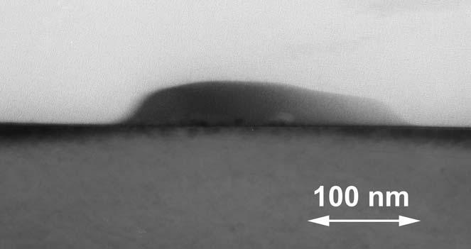
31 Epitaxial, tetragonal Pb(Zr 0.52 Ti 0.48 )O 3 nanoislands on SrTiO 3 made by CSD and a self-ordering process at 800 C SEM AFM 20 nm 500 nm 10 nm HREM PZT 2.5 µm Misfit Dislocations 0 nm [010] Nb:SrTiO 3 (STO) 4 nm From cross section electron microscopy (HREM): Truncated-pyramid nanoislands, average height: ~9 nm; average base length: ~50 nm.
 PZT STO c c a a δ = c-domain a PZT -a STO a STO = 3.4% (001) PZT [100] PZT (001) STO [100] STO 1 B. Noheda et al., Appl.")
32 Origin of misfit dislocations: misfit (δ) and c-axis orientation 4.15 a c Lattice Parameters (A) o Tetragonal Cubic 2 Cubic 1 PZT STO o T ( C) PZT STO c c a a δ = c-domain a PZT -a STO a STO = 3.4% (001) PZT [100] PZT (001) STO [100] STO 1 B. Noheda et al., Appl. Phys. Lett. 74, 2059 (1999); 2 S. Stemmer et al., Phys. Stat. Sol. (a) 147, 135 (1995).
![HREM investigations of misfit dislocations [010] -PbO](/docs-images/83/87618031/images/33-1.jpg "-(Zr,Ti)O 2 -SrO PZT STO T -TiO 2 -SrO Edge")

33 HREM investigations of misfit dislocations [010] -PbO -(Zr,Ti)O 2 -SrO PZT STO T -TiO 2 -SrO Edge Dislocation: Burgers vector (b) = <100> = ~4 Å 2 nm The PZT lattice around the dislocation core is strongly distorted!
34 Strain Field and Strain Energy of Edge Dislocations Edge Dislocation * y (r, θ) r θ x dislocation z dislocation Strain Field: * sin θ r ~b interface ( ) Strain Energy: * ~ (b interface ) 2 ln( ) h r r: dislocation core radius b ~ 5b * Elementary Dislocation Theory, J. Weertman and J. R. Weertman, Macmillian (New York), 1964.
35 Quantitative HREM measurements of strain fields * [010] Image of a perfect crystal: * PZT ΣH g exp{2πigr} ; g H g = A g exp{ip g } STO A g : amplitude P g : phase r : position in the image g : reciprocal lattice vector 2 nm * M. J. Hÿtch et al., Ultramicroscopy 74, 131 (1998); Microsc. Microanal. Microstruct. 8, 41 (1997).
36 Quantitative HREM Measurements of Strain Fields * Fourier Transform STO STO Image of a particular set of lattice fringes: * 2A g (r)cos{2πg r + P g (r)} PZT PZT * M. J. Hÿtch et al., Ultramicroscopy 74, 131 (1998); Microsc. Microanal. Microstruct. 8, 41 (1997).
37 Quantitative HREM Measurements of Strain Fields * Fourier Transform Image of a particular set of lattice fringes: * 2A g (r)cos{2πg. r + P g (r)} g g' 101 STO 101 PZT g = g - g' 2A g (r)cos{ 2π g. r + 2π g. r+p g (r)} Inverse FT Geometric Phase Gradient: P g (r) = 2π g * M. J. Hÿtch et al., Ultramicroscopy 74, 131 (1998); Microsc. Microanal. Microstruct. 8, 41 (1997).
} g 2A g (r)cos{ 2πg. r + 2π g. r+p g (r)} Inverse FT Geometric Phase Gradient: P g (r) = 2π g * M. J. Hÿtch et al., Ultramicroscopy 74, 131 (1998); Microsc. Microanal.")
38 Quantitative HREM Measurements of Strain Fields * Fourier Transform g 2 = 001 STO g 1 =101 STO Image of a particular set of lattice fringes: * 2A g (r)cos{2πg. r + P g (r)} g 2A g (r)cos{ 2πg. r + 2π g. r+p g (r)} Inverse FT Geometric Phase Gradient: P g (r) = 2π g * M. J. Hÿtch et al., Ultramicroscopy 74, 131 (1998); Microsc. Microanal. Microstruct. 8, 41 (1997).
 due to: (a) noise, (b) thickness, and/or (c) slight")
39 Quantitative HREM measurements of strain fields Geometric phase images (P g ) g 1 = 101 g 2 = 001 PZT PZT STO STO c a π 2 nm c a 2 nm 0 -π Phase fluctuations in the reference lattice (STO) due to: (a) noise, (b) thickness, and/or (c) slight misorientation.


40 Quantitative HREM Measurements of Strain Fields Displacement Field Images ( u x ) - u y = 2π ( )( ) a 2y 1 a 1x a 1y a 2x P g1 P g2 PZT PZT STO c a 2 nm = - 1 2π 1-1 STO c a 2 nm 0 1 PZT 0.5 PZT π STO c a 2 nm STO c a 2 nm 0 -π
41 Quantitative HREM Measurements of Strain Fields Strain Field Images (ε) * ε = ½ (e + e T ) e = ( e xx e xy ) e yy e yx = u x x u y x u x y ( ) u y y e - local distortion; e T - transpose of e. * M. J. Hÿtch et al., Ultramicroscopy 74, 131 (1998); Microsc. Microanal. Microstruct. 8, 41 (1997).
![Quantitative HREM measurements of strain fields Strain field images ε xx ε xy ε yy PZT T PZT T PZT T [001] STO [100] 4 nm STO 4 nm STO 4 nm [001] [001] [100] [100] 0.03 0-0.](/docs-images/83/87618031/images/42-0.jpg "03 In-plane (ε xx ), shear (ε xy ), and out-of-plane (ε yy ) strain fields predominantly localize on the PZT side, asymmetrically extending ~4 nm into the PZT nanoislands, because PZT is")
42 Quantitative HREM measurements of strain fields Strain field images ε xx ε xy ε yy PZT T PZT T PZT T [001] STO [100] 4 nm STO 4 nm STO 4 nm [001] [001] [100] [100] In-plane (ε xx ), shear (ε xy ), and out-of-plane (ε yy ) strain fields predominantly localize on the PZT side, asymmetrically extending ~4 nm into the PZT nanoislands, because PZT is softer than STO.

43 Impact of the strain fields on the polarization instability Partial volume V p of nanoislands affected by strain fields HREM [010] PZT ~8 nm STO ~4 nm 4 nm Plan-view ~50 nm [010] [100] Dislocation networks PZT Height ~10 nm g = [220] 60 nm ~8 nm V p ~ 0.5
 Piezoresponse force")

44 ZPFM signal (a. u.) Piezoresponse force microscopy (PFM) investigations AFM bias z P s PZT E STO Applied bias (V)
45 Piezoresponse force microscopy (PFM) investigations Partial volume V p of nanoislands affected by strain fields 150 PZT~10 nm PFM signal (a.u.) V p ~ Applied Bias (V)
46 Piezoresponse force microscopy (PFM) investigations Partial volume V p of nanoislands affected by strain fields PFM signal (a.u.) V p ~ 0.3 PZT~10 nm PZT~20 nm V p ~ Applied Bias (V)
 -100 V p ~ 0.6 0.5 Misfit dislocation FREE -10-5 0 5 10 STO Applied Bias (V) 3 nm")
47 Piezoresponse force microscopy (PFM) investigations Partial volume V p of nanoislands affected by strain fields PFM signal (a.u.) PZT~10 nm PZT~20 nm PTO~9 nm V p ~ 0.3 V p = 0 [010] -50 PbTiO 3 (PTO) -100 V p ~ Misfit dislocation FREE STO Applied Bias (V) 3 nm
 Interfacial misfit engineering is indispensable for obtaining nano-structured ferroelectrics with stable polarization. (Published in the February, 2004, issue of Nature Materials.")
48 Conclusions: (1) An interfacial strain field scenario for the polarization instability of ferroelectrics with confined dimensions is proposed by quantitative HREM and PFM measurements. (2) Interfacial misfit engineering is indispensable for obtaining nano-structured ferroelectrics with stable polarization. (Published in the February, 2004, issue of Nature Materials.) From a comment by Waser and Rüdiger in the same issue


49 September 2004: A thermodynamic model based on Landau-Devonshire formalism
50 (4) Microstructure and properties II: Microstructure and properties II: Interfacial dislocations and the mobility of 90 domain walls
O 3 T > T c T < T c Paraelectric (cubic) ~45 P s c a c a Thin-film capacitors:")
: 90 a/c domains switchable. *V.")
51 90 Domains in Ferroelectrics tetragonal Pb(Zr 0.4 Ti 0.6 )O 3 T > T c T < T c Paraelectric (cubic) ~45 P s c a c a Thin-film capacitors: 90 a/c domains elastically clamped by the substrate, therefore electrically inactive. Nanoislands* (~100 nm, lateral): 90 a/c domains switchable. *V. Nagarajan et al., Nature Mater. 2, 43 (2002).

52 Interaction of 90 Domains & Dislocations in Pb(Zr0.4Ti0.6)O3 Nanoislands? [010] a-domain c-domain Domain Domain Wall Wall ~45 T STO T T Ps Ps 4 nm 2 nm
 Angular separation ~1, (ii) Ferroelastic strain ~3.5%, (iii) Domain wall width ~1.5nm.* 2 nm Biaxial stress of 90 domain: ~5.")
53 90 Domains in Pb(Zr 0.4 Ti 0.6 )O 3 Nanoislands nm Courtesy of D. Shilo et al.* (i) Angular separation ~1, (ii) Ferroelastic strain ~3.5%, (iii) Domain wall width ~1.5nm.* 2 nm Biaxial stress of 90 domain: ~5.4 GPa *D. Shilo et al., Nature Mater. 3, 453 (2004).
, shear (ε xy ), and out-of-plane (ε yy ) strain fields")
 Domain wall as a compressively strained region embedded in strain free PZT.")
54 Strain Fields of 90 Domains: Geometric Phase Method* Strain Field Images (ε) ε xx ε xy ε yy PZT 2 nm PZT PZT [001] [001] [001] [100] [100] In-plane (ε xx ), shear (ε xy ), and out-of-plane (ε yy ) strain fields localized on the domain wall: (1) Extending ~2 ± 0.5 nm around the domain wall, (2) Domain wall as a compressively strained region embedded in strain free PZT. [100] *M.-W. Chu et al., Nature Mater. 3, 87 (2004).
![90 Domains + Interfacial Dislocations [010] PZT STO P s T P s 1.](/docs-images/83/87618031/images/55-0.jpg "Domain wall does NOT terminate on the dislocation core; 2.")
55 90 Domains + Interfacial Dislocations [010] PZT STO P s T P s 1. Domain wall does NOT terminate on the dislocation core; 2. Edge Dislocation: Burgers vector (b) = <001> = ~4 Å. In general case, b // interface!! 2 nm
![Strain Fields of 90 Domains + Interfacial Dislocations Strain Field Images (ε) ε xx ε xy ε yy PZT PZT PZT [001] STO [100] 4 nm [001] STO [100] 4 nm [001] STO [100] 4 nm 0.](/docs-images/83/87618031/images/56-0.jpg "03 In-plane (ε xx ), shear (ε xy ), and out-of-plane (ε yy ) strain fields : (1) Localized on domain wall and dislocation core, (2) Domain wall (compressive) elastically coupled to dislocation")
56 Strain Fields of 90 Domains + Interfacial Dislocations Strain Field Images (ε) ε xx ε xy ε yy PZT PZT PZT [001] STO [100] 4 nm [001] STO [100] 4 nm [001] STO [100] 4 nm 0.03 In-plane (ε xx ), shear (ε xy ), and out-of-plane (ε yy ) strain fields : (1) Localized on domain wall and dislocation core, (2) Domain wall (compressive) elastically coupled to dislocation core (tensile)
57 Impacts of Elastic Coupling: Electric Switching of 90 Domains Ground State PZT P s [010] P s PZT P s P s P s T STO 4 nm STO 4 nm + (1) Such in-plane climb of extra-half plane is energetically unfavorable;* (2) Interfacial dislocations (b interface) behave as pinning centers for 90 domain walls. * A. Yu. Emelyanov and N. A. Pertsev, Integ. Ferroelectrics 32, 343 (2001).
58 (5) Microstructure and properties III: Microstructure and properties III: The impact of interfaces on ferroelectric imprint in arrays
59 Regular arrays of polycrystalline PZT nanoislands As-prepared regular PZT arrays (SEM image) Patterned test structure 500 nm x 500 nm 250 nm x 250 nm 100 nm x 100 nm


60 Ferroelectric properties of polycrystalline PZT nanostructures PZT 500 nm x 500 nm 250 nm x 250 nm 100 nm x 100 nm PFM hysteresis curves of a 1 µm and 100 nm large nanostructure Switching without cross talk
61 Size-dependent imprint in regular arrays of polycrystalline PZT nanoislands Size-dependent polarization imprint 1000 nm 500 nm 250 nm 100 nm bias z P s PZT E STO PFM
 β = (34.5 ± 3.7) nm δ = (7.5 ± 4.")
62 Size-dependent imprint in regular arrays of polycrystalline PZT nanoislands Size-dependent polarization imprint - Phenomenological model Ω Offset -0.4 Ω = β β 2 1 d 2β 2 1 d δ 2δ 1 h 2δ + 1 h Cell size (nm) β = (34.5 ± 3.7) nm δ = (7.5 ± 4.5) nm
63 Regular arrays of epitaxial BaTiO 3 nanoislands Preparation of regular arrays by Pulsed laser deposition Array of latex spheres (SEM image) 1. Substrate; 2. Latex sphere; 3. Interstice SEM The result AFM
 4 2 Bias (V) 0-20 -10 0 10 20-2 a b c -4 PFM a - 45 nm thick, 230 nm wide b - 25 nm thick, 160 nm wide c - 25 nm thick, 500 nm wide Non-switchable layer, about 10 nm thick?")
64 Thickness-dependent imprint in regular arrays of epitaxial BaTiO 3 nanoislands Epitaxial structure (TEM after FIB) Thickness-dependent imprint d 33 (a. u.) 4 2 Bias (V) a b c -4 PFM a - 45 nm thick, 230 nm wide b - 25 nm thick, 160 nm wide c - 25 nm thick, 500 nm wide Non-switchable layer, about 10 nm thick? Interface-determined imprint?
65 Thickness-dependent imprint in regular arrays of epitaxial BaTiO 3 nanoislands HRTEM: Is there any interface-near structure modification??


66 Thickness-dependent imprint in regular arrays of epitaxial BaTiO 3 nanoislands Is it due to crystallization kinetics?


67 Modification of the interface-near region by a reaction-diffusion process SrBi 2 Ta 2 O 9 nanopyramid on SrTiO 3, crystallized at 950 C B.F. 022-D.F.
68 (6) Summary and outlook Ferroelectric nanostructures can be grown by a variety of physical and chemical methods. Nanoparticles in powders, and arrays of polycrystalline or epitaxial nanostructures on various substrates can be grown. Which method to choose depends on the envisaged properties. The real structure of the nanostructures considerably influences the physical properties. Interfaces, in particular, may have a strong impact: - Interfacial misfit dislocations were clearly shown to contribute to the size effect of epitaxial PZT nanoislands. Most probably they also hinder switching by pinning of 90 domains. - Structurally modified, non-switchable regions near interfaces can lead to size- or thickness-dependent imprint effects. From a combined application of high-resolution transmission electron microscopy and piezoresponse scanning force microscopy one can expect further progress in clarifying the role of the microstructure in nanostructured ferroelectrics.
69 Some publications C. Harnagea, M. Alexe, J. Schilling, J. Choi, R.B. Wehrspohn, D. Hesse, and U. Gösele, Mesoscopic ferroelectric cell arrays prepared by imprint lithography, Appl. Phys. Lett. 83 (2003) I. Szafraniak, C. Harnagea, R. Scholz, S. Bhattacharyya, D. Hesse, and M. Alexe, Ferroelectric epitaxial nanocrystals obtained by a self-patterning method Appl. Phys. Lett. 83 (2003) W. Ma, C. Harnagea, D. Hesse, and U. Gösele, Well-ordered arrays of pyramid-shaped ferroelectric BaTiO 3 nanostructures. Appl. Phys. Lett. 83 (2003) M.-W. Chu, I. Szafraniak, R. Scholz, D. Hesse, M. Alexe, and U. Gösele, Impact of misfit dislocations on the polarization instability of epitaxial nanostructured ferroelectric perovskites Nature Materials 3 (2004) W. Ma and D. Hesse, Polarization imprint in ordered arrays of epitaxial ferroelectric nanostructures Appl. Phys. Lett. 84 (2004) W. Ma and D. Hesse, Microstructure and piezoelectric properties of sub-80 nm high polycrystalline SrBi 2 Ta 2 O 9 nanostructures within well-ordered arrays Appl. Phys. Lett. 85 (2004), October issue. S.K. Lee, W. Lee, M. Alexe, K. Nielsch, D. Hesse, and U. Gösele, Well-ordered large-area arrays of epitaxial ferroelectric (Bi,La) 4 Ti 3 O 12 nanostructures fabricated by gold nanotube-membrane lithography Applied Physics Letters 86 (2005) (3p.)
 = 2.76 Å The equilibrium distance of misfit dislocations is P = b / f. f Obviously, b 3.95 Å. The misfit is f = 2 (a( f - a s ) / (a( f + a s ). a BTO = 3.992 Å; c BTO = 4.")
70 Thickness-dependent imprint in regular arrays of epitaxial BaTiO 3 nanoislands Spacing of misfit dislocations varies extensively. Example for narrow spacing: BaTiO 3 SrTiO 3 3nm 12.1 nm 11.7 nm d(110) = 2.76 Å The equilibrium distance of misfit dislocations is P = b / f. f Obviously, b 3.95 Å. The misfit is f = 2 (a( f - a s ) / (a( f + a s ). a BTO = Å; c BTO = Å; a STO = Å. (a) If BaTiO 3 is c-axis-up oriented: f = %. Hence P = b / f = 3.95 / = 180 Å. (b) If BaTiO 3 is a-axis-up oriented: f = %. Hence P = b / f = 3.95 / = 120 Å.

71 Thickness-dependent imprint in regular arrays of epitaxial BaTiO 3 nanoislands HRTEM: What is the interface-near structure modification like? P s P s A 10 nm thin layer having partly in-plane, partly out-of-plane polarization?
 Depolarization Field (E dp ) Perovskite + + + + + + + + + + + + + + + + + + + + + + + a p = ~3.8 Å P s E dp P s + + * A. Roelofs et al., Appl. Phys. Lett.")
72 The polarization instability: Size effect in nano-ferroelectrics? Bulk Nanoisland/Film Bulk t: ~ µm t: < ~4 nm * Nanoisland/ Film PbTiO 3 (S. V. Kalinin and D. A. Bonnel) Depolarization Field (E dp ) Perovskite a p = ~3.8 Å P s E dp P s + + * A. Roelofs et al., Appl. Phys. Lett. 81, 5231 (2002).
73 A new approach: Metal nanotube membranes as deposition masks Hexagonal lattice Back side view Back side view 7 µm 1 µm 7 µm 600 nm Square lattice Front side view 3 µm d 3 µm 3 µm 500 nm Example: d = 280 nm

 TEM SEM d 33 (pm/v) 100 75 50 25 0-25 -50-75 -100 WL03 PFM @ 36.")
74 A new approach: Metal nanotube membranes as deposition masks Large-area area ferroelectric PZT and BLT nanodot arrays S.K. Lee, W. Lee, M. Alexe, K. Nielsch, D. Hesse, and U. Gösele, Applied Physics Letters 86 (2005) (3p.) TEM SEM d 33 (pm/v) WL khz ATEC-FM PFM Applied Bias (V)
From 180º stripe domains to more exotic patterns of polarization in ferroelectric nanostructures. A first principles view
 From 180º stripe domains to more exotic patterns of polarization in ferroelectric nanostructures. A first principles view Pablo Aguado-Puente Javier Junquera Ferroelectricity: Basic definitions Existence
Piezoelectric materials for MEMS applications Hiroshi Funakubo Tokyo Institute of Technology
 Piezoelectric materials for MEMS applications Hiroshi Funakubo Tokyo Institute of Technology MEMS Engineer Forum 2016/5/11 11:50-12:15 Content 1. Introduction 2. Processing 3. Materials Matter Content
Supplementary Figures:
 Supplementary Figures: Supplementary Figure 1 Cross-sectional morphology and Chemical composition. (a) A low-magnification dark-field TEM image shows the cross-sectional morphology of the BWO thin film
Nanostructured Ferroelectrics: Fabrication and Structure Property Relations
 Nanostructured Ferroelectrics: Fabrication and Structure Property Relations Hee Han, * Yunseok Kim, Marin Alexe, Dietrich Hesse, and Woo Lee * With the continued demand for ultrahigh density ferroelectric
5. Building Blocks I: Ferroelectric inorganic micro- and nano(shell) tubes
 tubes") 5. Building Blocks I: Ferroelectric inorganic micro- and nano(shell) tubes 5.1 New candidates for nanoelectronics: ferroelectric nanotubes In this chapter, one of the core elements for a complex building
5. Building Blocks I: Ferroelectric inorganic micro- and nano(shell) tubes 5.1 New candidates for nanoelectronics: ferroelectric nanotubes In this chapter, one of the core elements for a complex building
Epitaxial piezoelectric heterostructures for ultrasound micro-transducers
 15 th Korea-U.S. Forum on Nanotechnology Epitaxial piezoelectric heterostructures for ultrasound micro-transducers Seung-Hyub Baek Center for Electronic Materials Korea Institute of Science and Technology
SUPPLEMENTARY MATERIAL
 SUPPLEMENTARY MATERIAL Multiphase Nanodomains in a Strained BaTiO3 Film on a GdScO3 Substrate Shunsuke Kobayashi 1*, Kazutoshi Inoue 2, Takeharu Kato 1, Yuichi Ikuhara 1,2,3 and Takahisa Yamamoto 1, 4
Microstructure evolution during BaTiO 3 formation by solid-state reactions on rutile single crystal surfaces
 Journal of the European Ceramic Society 25 (2005) 2201 2206 Microstructure evolution during BaTiO 3 formation by solid-state reactions on rutile single crystal surfaces Andreas Graff a,, Stephan Senz a,
Aberration-corrected TEM studies on interface of multilayered-perovskite systems
 Aberration-corrected TEM studies on interface of multilayered-perovskite systems By Lina Gunawan (0326114) Supervisor: Dr. Gianluigi Botton November 1, 2006 MSE 702(1) Presentation Outline Literature Review
Lead Titanate films on Dysprosium Scandate with a Strontium Ruthenate Buffer Layer grown by Pulsed Laser Deposition
 Lead Titanate films on Dysprosium Scandate with a Strontium Ruthenate Buffer Layer grown by Pulsed Laser Deposition By: Brian Smith November 2009 Supervised by: Beatriz Noheda Abstract Ferroelectric materials
Control of periodic ferroelastic domains in ferroelectric Pb1-xSrxTiO3 thin films for nanoscaled
 University of Groningen Control of periodic ferroelastic domains in ferroelectric Pb1-xSrxTiO3 thin films for nanoscaled memory devices Nesterov, Oleksiy IMPORTANT NOTE: You are advised to consult the
Investigation of microstructure and piezoelectric properties of Zr- and Smdoped PbTiO 3 nanostructured thin films derived by sol gel technology
 Sensors and Actuators B 109 (2005) 97 101 Investigation of microstructure and piezoelectric properties of Zr- and Smdoped PbTiO 3 nanostructured thin films derived by sol gel technology Arturas Ulcinas
Chapter 3 Chapter 4 Chapter 5
 Preamble In recent years bismuth-based, layer-structured perovskites such as SrBi 2 Nb 2 O 9 (SBN) and SrBi 2 Ta 2 O 9 (SBT) have been investigated extensively, because of their potential use in ferroelectric
Effect of interfacial dislocations on ferroelectric phase stability and domain morphology in a thin film a phase-field model
 JOURNAL OF APPLIED PHYSICS VOLUME 94, NUMBER 4 15 AUGUST 2003 Effect of interfacial dislocations on ferroelectric phase stability and domain morphology in a thin film a phase-field model S. Y. Hu, Y. L.
Fabrication of isolated ferroelectric nanostructures
 Mat. Res. Soc. Symp. Proc. Vol. 740 2003 Materials Research Society I10.3.1 Fabrication of isolated ferroelectric nanostructures S. Bhattacharyya (a), Soma Chattopadhyay ( ) and M. Alexe Max Planck Institute
Citation JOURNAL OF APPLIED PHYSICS (2003),
,") Crystallographic characterization o Titlefilms with different Zr/Ti ratio gr magnetron sputtering Author(s) Kanno, I; Kotera, H; Wasa, K; Matsu Takayama, R Citation JOURNAL OF APPLIED PHYSICS (2003), Issue
Crystallographic characterization o Titlefilms with different Zr/Ti ratio gr magnetron sputtering Author(s) Kanno, I; Kotera, H; Wasa, K; Matsu Takayama, R Citation JOURNAL OF APPLIED PHYSICS (2003), Issue
High-resolution Characterization of Organic Ultrathin Films Using Atomic Force Microscopy
 High-resolution Characterization of Organic Ultrathin Films Using Atomic Force Microscopy Jing-jiang Yu Nanotechnology Measurements Division Agilent Technologies, Inc. Atomic Force Microscopy High-Resolution
Nanostructure. Materials Growth Characterization Fabrication. More see Waser, chapter 2
 Nanostructure Materials Growth Characterization Fabrication More see Waser, chapter 2 Materials growth - deposition deposition gas solid Physical Vapor Deposition Chemical Vapor Deposition Physical Vapor
APPENDIX A Landau Free-Energy Coefficients
 APPENDIX A Landau Free-Energy Coefficients Long-Qing Chen Department of Materials Science and Engineering, The Pennsylvania State University, University Park, Pennsylvania 180 USA The thermodynamics of
Effect of substrate-induced strains on the spontaneous polarization of epitaxial BiFeO 3 thin films
 JOURNAL OF APPLIED PHYSICS 11, 11415 27 Effect of substrate-induced strains on the spontaneous polarization of epitaxial 3 thin films J. X. Zhang, a Y. L. Li, Y. Wang, Z. K. Liu, and L. Q. Chen Department
Classification of Dielectrics & Applications
 Classification of Dielectrics & Applications DIELECTRICS Non-Centro- Symmetric Piezoelectric Centro- Symmetric Pyroelectric Non- Pyroelectric Ferroelectrics Non-Ferroelectric Piezoelectric Effect When
Strain-induced single-domain growth of epitaxial SrRuO 3 layers on SrTiO 3 : a high-temperature x-ray diffraction study
 Strain-induced single-domain growth of epitaxial SrRuO 3 layers on SrTiO 3 : a high-temperature x-ray diffraction study Arturas Vailionis 1, Wolter Siemons 1,2, Gertjan Koster 1 1 Geballe Laboratory for
Depth profile study of ferroelectric PbZr 0.2 Ti 0.8 O 3 films
 JOURNAL OF APPLIED PHYSICS VOLUME 92, NUMBER 11 1 DECEMBER 2002 Depth profile study of ferroelectric PbZr 0.2 Ti 0.8 O 3 films Y. Li, V. Nagarajan, S. Aggarwal, R. Ramesh, L. G. Salamanca-Riba, and L.
A Hydrothermally Deposited Epitaxial PbTiO 3 Thin Film on SrRuO 3 Bottom Electrode for the Ferroelectric Ultra-High Density Storage Medium
 Integrated Ferroelectrics, 64: 247 257, 2004 Copyright C Taylor & Francis Inc. ISSN: 1058-4587 print/ 1607-8489 online DOI: 10.1080/10584580490894645 A Hydrothermally Deposited Epitaxial PbTiO 3 Thin Film
Thin Film Bi-based Perovskites for High Energy Density Capacitor Applications
 ..SKELETON.. Thin Film Bi-based Perovskites for High Energy Density Capacitor Applications Colin Shear Advisor: Dr. Brady Gibbons 2010 Table of Contents Chapter 1 Introduction... 1 1.1 Motivation and Objective...
Roger Johnson Structure and Dynamics: Displacive phase transition Lecture 9
 9.1. Summary In this Lecture we will consider structural phase transitions characterised by atomic displacements, which result in a low temperature structure that is distorted compared to a higher temperature,
Epitaxial integration of perovskite-based multifunctional oxides on silicon q
 Available online at www.sciencedirect.com Acta Materialia xxx (2012) xxx xxx www.elsevier.com/locate/actamat Epitaxial integration of perovskite-based multifunctional oxides on silicon q Seung-Hyub Baek,
Nanotechnology Nanofabrication of Functional Materials. Marin Alexe Max Planck Institute of Microstructure Physics, Halle - Germany
 Nanotechnology Nanofabrication of Functional Materials Marin Alexe Max Planck Institute of Microstructure Physics, Halle - Germany Contents Part I History and background to nanotechnology Nanoworld Nanoelectronics
Functional Perovskites From Epitaxial Films to Nanostructured Arrays**
 DOI: 10.1002/adfm.200800560 Functional Perovskites From Epitaxial Films to Nanostructured Arrays** By Ionela Vrejoiu, Marin Alexe, Dietrich Hesse,* and Ulrich Gösele Functional perovskite materials gain
Colossal electroresistance in metal/ferroelectric/semiconductor. tunnel diodes for resistive switching memories
 Colossal electroresistance in metal/ferroelectric/semiconductor tunnel diodes for resistive switching memories Zheng Wen, Chen Li, Di Wu*, Aidong Li and Naiben Ming National Laboratory of Solid State Microstructures
Dielectric, Piezoelectric and Nonlinear Optical Properties of Lead Titanate based Ferroelectric Thin films
 Dielectric, Piezoelectric and Nonlinear Optical Properties of Lead Titanate based Ferroelectric Thin films Ferroelectric oxides with perovskite structure has gained lot of interest from research as well
Local Piezoelectric Properties of Oriented PZT Based Ferroelectric Thin Films
 Ferroelectrics, 335:191 199, 2006 Copyright Taylor & Francis Group, LLC ISSN: 0015-0193 print / 1563-5112 online DOI: 10.1080/00150190600691353 Local Piezoelectric Properties of Oriented PZT Based Ferroelectric
File Name: Supplementary Information Description: Supplementary Figures, Supplementary Table, Supplementary Notes and Supplementary References.
 File Name: Supplementary Information Description: Supplementary Figures, Supplementary Table, Supplementary Notes and Supplementary References. File Name: Supplementary Movie 1 Description: Projections
G. Ravichandran Aeronautics & Mechanical Engineering Graduate Aeronautical Laboratories California Institute of Technology
 Multi-Disciplinary University Initiative Army Research Office Engineering Microstructural Complexity in Ferroelectric Devices Mechanical Characterization G. Ravichandran Aeronautics & Mechanical Engineering
Room-temperature tunable microwave properties of strained SrTiO 3 films
 JOURNAL OF APPLIED PHYSICS VOLUME 96, NUMBER 11 1 DECEMBER 2004 Room-temperature tunable microwave properties of ed SrTiO 3 films Wontae Chang, a) Steven W. Kirchoefer, Jeffrey M. Pond, Jeffrey A. Bellotti,
Transformation dependence of lead zirconate titanate (PZT) as shown by PiezoAFM surface mapping of Sol-gel produced PZT on various substrates.
 as shown by PiezoAFM surface mapping of Sol-gel produced PZT on various substrates.") Transformation dependence of lead zirconate titanate (PZT) as shown by PiezoAFM surface mapping of Sol-gel produced PZT on various substrates. Abstract S. Dunn and R. W. Whatmore Building 70, Nanotechnology,
Transformation dependence of lead zirconate titanate (PZT) as shown by PiezoAFM surface mapping of Sol-gel produced PZT on various substrates. Abstract S. Dunn and R. W. Whatmore Building 70, Nanotechnology,
Electric displacement as the fundamental variable in electronic-structure calculations
 Electric displacement as the fundamental variable in electronic-structure calculations CECAM - Centre Européen de Calcul Atomique et Moléculaire EPF Lausanne, Switzerland Conference UC Davis, 6/23/2009
A Nanoscale Shape Memory Oxide
 A Nanoscale Shape Memory Oxide Jinxing Zhang 1,2*, Xiaoxing Ke 3*, Gaoyang Gou 4, Jan Seidel 2,5, Bin Xiang 6,9, Pu Yu 2,7, Wen-I Liang 8, Andrew M. Minor 9,10, Ying-hao Chu 8, Gustaaf Van Tendeloo 3,
Materials 218/UCSB: Phase transitions and polar materials
 Materials 218/UCSB: Phase transitions and polar materials Ram Seshadri (seshadri@mrl.ucsb.edu) Background: Intrinsic stability of thermodynamic systems (after H. B. Callen, Thermodynamics and an introduction
Micron 43 (2012) Contents lists available at SciVerse ScienceDirect. Micron. j our na l ho me p age:
 Contents lists available at SciVerse ScienceDirect. Micron. j our na l ho me p age:") Micron 43 (2012) 1121 1126 Contents lists available at SciVerse ScienceDirect Micron j our na l ho me p age: www.elsevier.com/locate/micron Direct observation of ferroelectric domain switching in varying
Micron 43 (2012) 1121 1126 Contents lists available at SciVerse ScienceDirect Micron j our na l ho me p age: www.elsevier.com/locate/micron Direct observation of ferroelectric domain switching in varying
Structural and electrical characterization of epitaxial, large area ferroelectric films of Ba 2 Bi 4 Ti 5 O 18 grown by pulsed excimer laser ablation
 JOURNAL OF APPLIED PHYSICS VOLUME 87, NUMBER 6 15 MARCH 2000 Structural and electrical characterization of epitaxial, large area ferroelectric films of Ba 2 Bi 4 Ti 5 O 18 grown by pulsed excimer laser
Fabrication at the nanoscale for nanophotonics
 Fabrication at the nanoscale for nanophotonics Ilya Sychugov, KTH Materials Physics, Kista silicon nanocrystal by electron beam induced deposition lithography Outline of basic nanofabrication methods Devices
Recent Developments in Magnetoelectrics Vaijayanti Palkar
 Recent Developments in Magnetoelectrics Vaijayanti Palkar Department of Condensed Matter Physics & Materials Science Tata Institute of Fundamental Research Mumbai 400 005, India. Tata Institute of Fundamental
High tunable dielectric response of Pb 0.87 Ba 0.1 La 0.02 (Zr 0.6 Sn 0.33 Ti 0.07 ) O 3 thin film
 O 3 thin film") Journal of Applied Physics, 2010, Volume 108, Issue 4, paper number 044107 High tunable dielectric response of Pb 0.87 Ba 0.1 La 0.02 (Zr 0.6 Sn 0.33 Ti 0.07 ) O 3 thin film T. M. Correia and Q. Zhang*
Journal of Applied Physics, 2010, Volume 108, Issue 4, paper number 044107 High tunable dielectric response of Pb 0.87 Ba 0.1 La 0.02 (Zr 0.6 Sn 0.33 Ti 0.07 ) O 3 thin film T. M. Correia and Q. Zhang*
Photovoltaic Enhancement Due to Surface-Plasmon Assisted Visible-Light. Absorption at the Inartificial Surface of Lead Zirconate-Titanate Film
 Photovoltaic Enhancement Due to Surface-Plasmon Assisted Visible-Light Absorption at the Inartificial Surface of Lead Zirconate-Titanate Film Fengang Zheng, a,b, * Peng Zhang, a Xiaofeng Wang, a Wen Huang,
Introduction to solid state physics
 PHYS 342/555 Introduction to solid state physics Instructor: Dr. Pengcheng Dai Professor of Physics The University of Tennessee (Room 407A, Nielsen, 974-1509) Chapter 13: Dielectrics and ferroelectrics
Newcastle University eprints
 Newcastle University eprints Ponon NK, Appleby DJR, Arac E, Kwa KSK, Goss JP, Hannemann U, Petrov PK, Alford NM, O'Neill A. Impact of Crystalline Orientation on the Switching Field in Barium Titanate Using
PHASE-FIELD SIMULATION OF DOMAIN STRUCTURE EVOLUTION IN FERROELECTRIC THIN FILMS
 Mat. Res. Soc. Symp. Proc. Vol. 652 2001 Materials Research Society PHASE-FIELD SIMULATION OF DOMAIN STRUCTURE EVOLUTION IN FERROELECTRIC THIN FILMS Y. L. Li, S. Y. Hu, Z. K. Liu, and L. Q. Chen Department
JOURNAL OF APPLIED PHYSICS 101,
 JOURNAL OF APPLIED PHYSICS 101, 054118 2007 Growth, microstructure, and ferroelectric properties of Pb Zr 0.4 Ti 0.6 O 3 /PbZrO 3 superlattices prepared on SrTiO 3 100 substrates by pulsed laser deposition
Domain Nucleation And Relaxation Kinetics In Ferroelectric Thin Films. Ramesh
 Domain Nucleation And Relaxation Kinetics In Ferroelectric Thin Films C. S. Ganpule a), V. Nagarajan, S. B. Ogale, A. L. Roytburd, E. D. Williams and R. Ramesh Materials Research Science and Engineering
Adaptive ferroelectric states in systems with low domain wall energy: Tetragonal microdomains
 Adaptive ferroelectric states in systems with low domain wall energy: Tetragonal microdomains Y. M. Jin, Y. U. Wang, A. G. Khachaturyan, J. F. Li, and D. Viehland Citation: Journal of Applied Physics 94,
Table of Contents. Chapter 1. Dielectricity, Piezoelectricity, Pyroelectricity and Ferroelectricity... 1
 Preface... General Introduction... xiii xvii Chapter 1. Dielectricity, Piezoelectricity, Pyroelectricity and Ferroelectricity.... 1 1.1. Crystal structure... 1 1.1.1. Crystal = lattice + pattern... 1 1.1.2.
Stability of a Ferroelectric Phase with Electrical Domains in Multilayers
 Stability of a Ferroelectric Phase with Electrical Domains in Multilayers I. B. Misirlioglu Faculty of Engineering and Natural Sciences, Sabanci University, Tuzla/Orhanli 34956 Istanbul, Turkey Multilayer
Supplementary Information
 Supplementary Information Large Electrocaloric Effect in Relaxor Ferroelectric and Antiferroelectric Lanthanum Doped Lead Zirconate Titanate Ceramics Biao Lu, Peilian Li, Zhenghua Tang, Yingbang Yao, Xingsen
JOHN G. EKERDT RESEARCH FOCUS
 JOHN G. EKERDT RESEARCH FOCUS We study the surface, growth and materials chemistry of metal, dielectric, ferroelectric, and polymer thin films. We seek to understand and describe nucleation and growth
Experimental methods in Physics. Electron Microscopy. Basic Techniques (MEP-I) SEM, TEM
 SEM, TEM") Experimental methods in Physics Electron Microscopy Basic Techniques (MEP-I) SEM, TEM Advanced Techniques (MEP-II) HR-TEM, STEM Analytical-TEM 3D-Microscopy Spring 2012 Experimental Methods in Physics
Experimental methods in Physics Electron Microscopy Basic Techniques (MEP-I) SEM, TEM Advanced Techniques (MEP-II) HR-TEM, STEM Analytical-TEM 3D-Microscopy Spring 2012 Experimental Methods in Physics
Structural dynamics of PZT thin films at the nanoscale
 Mater. Res. Soc. Symp. Proc. Vol. 902E 2006 Materials Research Society 0902-T06-09.1 Structural dynamics of PZT thin films at the nanoscale Alexei Grigoriev 1, Dal-Hyun Do 1, Dong Min Kim 1, Chang-Beom
1. Chapter 1: Introduction
 1. Chapter 1: Introduction Non-volatile memories with ferroelectric capacitor materials are also known as ferroelectric random access memories (FRAMs). Present research focuses on integration of ferroelectric
Si, X. X. Xi, and Q. X. JIA
 LA-UR-01-1929 Approved for public release; distribution is unlimited. Title: DIELECTRIC PROPERTIES OF Ba0.6Sr0.4TiO3 THIN FILMS WITH VARIOUS STRAIN STATES Author(s): B. H. PARK, E. J. PETERSON, J. LEE,
Ferroelectricity. Phase transition. Material properties. 4/12/2011 Physics 403 Spring
 Ferroelectricity. Phase transition. Material properties 4/12/211 Physics 43 Spring 211 1 Ferroelectricity. outline Ferroelectricity. Definition Discovery Main properties Phenomenological theory Some materials
Photonic/Plasmonic Structures from Metallic Nanoparticles in a Glass Matrix
 Excerpt from the Proceedings of the COMSOL Conference 2008 Hannover Photonic/Plasmonic Structures from Metallic Nanoparticles in a Glass Matrix O.Kiriyenko,1, W.Hergert 1, S.Wackerow 1, M.Beleites 1 and
NANOSCALE PHENOMENA IN FERROELECTRIC THIN FILMS
 NANOSCALE PHENOMENA IN FERROELECTRIC THIN FILMS NANOSCALEPHENOMENAIN FERROELECTRIC THIN FILMS edited by Seungbum Hong Samsung Advanced Institute oftechnology, Korea SPRINGER-SCIENCE+BUSINESS MEDIA, LLC
Using the surface spontaneous depolarization field of ferroelectrics to direct the assembly of virus particles
 Appl. Phys. Lett. Vol 85, Issue 16, 3537 (2004) Using the surface spontaneous depolarization field of ferroelectrics to direct the assembly of virus particles Working Title: Directed assembly of biological
Matias Bargheer. Examples of Ultrafast X-ray Diffraction Experimens: Synchrotron vs. Laser-Plasma Sources
 Matias Bargheer Examples of Ultrafast X-ray Diffraction Experimens: Synchrotron vs. Laser-Plasma Sources Some details of the setup: BESSYII + Plasma VSR Ultrafast heat transport on nm length scale Inhomogeneous
Morphological evolution of single-crystal ultrathin solid films
 Western Kentucky University From the SelectedWorks of Mikhail Khenner March 29, 2010 Morphological evolution of single-crystal ultrathin solid films Mikhail Khenner, Western Kentucky University Available
ELECTRONICS DEVICES AND MATERIALS
 2-2-2 ELECTRONICS DEVICES AND MATERIALS Atsunori KAMEGAWA SYLLABUS! Introduction to materials structure and dielectric physics (04/27)! Ferroelectricity involved in structural phase transitions (05/25)
Bridging to the Continuum Scale for Ferroelectric Applications
 Bridging to the Continuum Scale for Ferroelectric Applications Shanfu Zheng and Alberto Cuitiño Mechanical and Aerospace Engineering, Rutgers University Alejandro Strachan Materials Engineering, Purdue
Nano fabrication and optical characterization of nanostructures
 Introduction to nanooptics, Summer Term 2012, Abbe School of Photonics, FSU Jena, Prof. Thomas Pertsch Nano fabrication and optical characterization of nanostructures Lecture 12 1 Optical characterization
Laser Annealing of MOCVD Deposited Ferroelectric SrBi 2 Ta 2 O 9, Pb(Zr X Ti 1-X )O 3 and CeMnO 3 Thin Films
O 3 and CeMnO 3 Thin Films") 1 Laser Annealing of MOCVD Deposited Ferroelectric SrBi 2 Ta 2 O 9, Pb(Zr X Ti 1-X )O 3 and CeMnO 3 Thin Films N.M. Sbrockey 1, J.D. Cuchiaro 1, L.G. Provost 1, C.E. Rice 1, S. Sun 1, G.S. Tompa 1, R.L.
1 Laser Annealing of MOCVD Deposited Ferroelectric SrBi 2 Ta 2 O 9, Pb(Zr X Ti 1-X )O 3 and CeMnO 3 Thin Films N.M. Sbrockey 1, J.D. Cuchiaro 1, L.G. Provost 1, C.E. Rice 1, S. Sun 1, G.S. Tompa 1, R.L.
There's Plenty of Room at the Bottom
 There's Plenty of Room at the Bottom 12/29/1959 Feynman asked why not put the entire Encyclopedia Britannica (24 volumes) on a pin head (requires atomic scale recording). He proposed to use electron microscope
One-dimensional ferroelectrics: Nanowires and nanotubes
 One-dimensional ferroelectrics: Nanowires and nanotubes M. Alexe and D. Hesse Max Planck Institute of Microstructure Physics, D-06120 Halle, Germany Abstract An overview of some general features of the
Fabrication / Synthesis Techniques
 Quantum Dots Physical properties Fabrication / Synthesis Techniques Applications Handbook of Nanoscience, Engineering, and Technology Ch.13.3 L. Kouwenhoven and C. Marcus, Physics World, June 1998, p.35
Domain switching and electromechanical properties of pulse poled Pb Zn 1Õ3 Nb 2Õ3 O 3 PbTiO 3 crystals
 JOURNAL OF APPLIED PHYSICS VOLUME 89, NUMBER 1 1 JANUARY 2001 Domain switching and electromechanical properties of pulse poled Pb Zn 1Õ3 Nb 2Õ3 O 3 PbTiO 3 crystals Hanxing Yu, Venkat Gopalan, Jürgen Sindel,
A Novel Self-aligned and Maskless Process for Formation of Highly Uniform Arrays of Nanoholes and Nanopillars
 Nanoscale Res Lett (2008) 3: 127 DOI 10.1007/s11671-008-9124-6 NANO EXPRESS A Novel Self-aligned and Maskless Process for Formation of Highly Uniform Arrays of Nanoholes and Nanopillars Wei Wu Æ Dibyendu
Ferroelectricity in Strain-Free SrTiO 3 Thin Films
 Ferroelectricity in Strain-Free SrTiO 3 Thin Films H. W. Jang, 1 A. Kumar, 2 S. Denev, 2 M. D. Biegalski, 3 P. Maksymovych, 3 C.W. Bark, 1 C. T. Nelson, 4 C. M. Folkman, 1 S. H. Baek, 1 N. Balke, 3 C.
Stabilization of highly polar BiFeO 3 like structure: a new interface design route for enhanced ferroelectricity in artificial perovskite superlattice
 Stabilization of highly polar BiFeO 3 like structure: a new interface design route for enhanced ferroelectricity in artificial perovskite superlattice Speaker: Xifan Wu Temple University Outline Part I.
JOURNAL OF APPLIED PHYSICS 102,
 JOURNAL OF APPLIED PHYSICS 102, 044111 2007 Microstructure and electrical properties of 120 O -oriented and of 001 O -oriented epitaxial antiferroelectric PbZrO 3 thin films on 100 SrTiO 3 substrates covered
Depolarization of a piezoelectric film under an alternating current field
 JOURNAL OF APPLIED PHYSICS 101, 054108 2007 Depolarization of a piezoelectric film under an alternating current field K. W. Kwok, a M. K. Cheung, H. L. W. Chan, and C. L. Choy Department of Applied Physics
Defect structure and oxygen diffusion in PZT ceramics
 Defect structure and oxygen diffusion in PZT ceramics Adam Georg Balogh Institute of Materials Science Technische Universität Darmstadt A. G. Balogh Folie 1 Introduction Ferroelectrics are of great technical
Monte Carlo Simulation of Ferroelectric Domain Structure: Electrostatic and Elastic Strain Energy Contributions
 Monte Carlo Simulation of Ferroelectric Domain Structure: Electrostatic and Elastic Strain Energy Contributions B.G. Potter, Jr., B.A. Tuttle, and V. Tikare Sandia National Laboratories Albuquerque, NM
Atomic Resolution Interfacial Structure of Lead-free Ferroelectric
 Atomic Resolution Interfacial Structure of Lead-free Ferroelectric K 0.5 Na 0.5 NbO 3 Thin films Deposited on SrTiO 3 Chao Li 1, Lingyan Wang 1*, Zhao Wang 2, Yaodong Yang 2, Wei Ren 1 and Guang Yang 1
Ferroelectricity. Phase transition. Material properties
 Ferroelectricity. Phase transition. Material properties BaTiO 3 DKDP KDP PZN-PT(9%) PMN-PT(30%) PMN-PT(40%) 4/1/2016 Physics 403 Spring 2016 1 Ferroelectricity. outline Ferroelectricity. Definition Discovery
Thermodynamic theory of epitaxial ferroelectric thin films with dense domain structures
 Thermodynamic theory of epitaxial ferroelectric thin films with dense domain structures V. G. Koukhar, N. A. ertsev,,, and R. Waser, A.F. Ioffe hysico-technical Institute, Russian Academy of ciences, 9
Effects of niobium doping on the piezoelectric properties of sol gel-derived lead zirconate titanate films
 JOURNAL OF APPLIED PHYSICS VOLUME 95, NUMBER 3 1 FEBRUARY 2004 Effects of niobium doping on the piezoelectric properties of sol gel-derived lead zirconate titanate films K. W. Kwok, a) R. C. W. Tsang,
Complex Nanostructures by Atomic Layer Deposition. Kornelius Nielsch.
 Complex Nanostructures by Atomic Layer Deposition Kornelius Nielsch Institute of Applied Physics, University of Hamburg (Germany) knielsch@physnet.uni-hamburg.de Outline History and Principle Ferromagnetic
Solid State Science and Technology, Vol. 13, No 1 & 2 (2005) ISSN
 ISSN") FABRICATION OF Bi-Ti-O THIN FILM PRESSURE SENSOR PREPARED BY ELECTRON BEAM EVAPORATION METHOD Chong Cheong Wei, Muhammad Yahaya and Muhamad Mat Salleh Institue of Microengineering and Nanoelectronics,
FABRICATION OF Bi-Ti-O THIN FILM PRESSURE SENSOR PREPARED BY ELECTRON BEAM EVAPORATION METHOD Chong Cheong Wei, Muhammad Yahaya and Muhamad Mat Salleh Institue of Microengineering and Nanoelectronics,
ACTA FERROELECTRIC PERFORMANCE FOR NANOMETER SCALED DEVICES. Maxim Plekh C 372 UNIVERSITATIS OULUENSIS OULU 2010 TECHNICA
 OULU 2010 C 372 ACTA Maxim Plekh UNIVERSITATIS OULUENSIS C TECHNICA FERROELECTRIC PERFORMANCE FOR NANOMETER SCALED DEVICES UNIVERSITY OF OULU, FACULTY OF TECHNOLOGY, DEPARTMENT OF ELECTRICAL AND INFORMATION
Synthesis and Characterization of Ferroic and Multiferroic Nanostructures by Liquid Phase Deposition
 University of New Orleans ScholarWorks@UNO University of New Orleans Theses and Dissertations Dissertations and Theses Fall 12-15-2012 Synthesis and Characterization of Ferroic and Multiferroic Nanostructures
1 Dielectric Properties of Polar Oxides. Abstract. 1.1 Introduction. Ulrich Böttger
 1 Dielectric Properties of Polar Oxides Ulrich Böttger Institut für Werkstoffe der Elektrotechnik, RWTH Aachen, Germany Abstract This chapter gives an introduction to the class of polar oxides. Basic principles
SOFT-MODE PHONONS in SrTiO 3 THIN FILMS STUDIED by FAR-INFRARED ELLIPSOMETRY and RAMAN SCATTERING
 SOFT-MODE PHONONS in SrTiO 3 THIN FILMS STUDIED by FAR-INFRARED ELLIPSOMETRY and RAMAN SCATTERING A. A. SIRENKO *, C. BERNHARD **, A. GOLNIK **, I. A. AKIMOV *, A. M. CLARK *, J.-H. HAO *, and X. X. XI
Transduction Based on Changes in the Energy Stored in an Electrical Field
 Lecture 7-1 Transduction Based on Changes in the Energy Stored in an Electrical Field - Electrostriction The electrostrictive effect is a quadratic dependence of strain or stress on the polarization P
Physics and Material Science of Semiconductor Nanostructures
 Physics and Material Science of Semiconductor Nanostructures PHYS 570P Prof. Oana Malis Email: omalis@purdue.edu Course website: http://www.physics.purdue.edu/academic_programs/courses/phys570p/ Lecture
CHAPTER-1 INTRODUCTION
 CHAPTER-1 INTRODUCTION 1.1 OVERVIEW In today s microelectronics computer industry, various types of memories are used for the data storage. Generally, memories are categorized into volatile and non-volatile.
Marin Alexe. Personal Information:
 Max Planck Institute of Microstructure Physics Weinberg 2 D-06120 Halle (Saale) Germany Tel: +49-345-5582-705 Fax: +49-345-5511-223 email: malexe@mpi-halle.de http://ww.mpi-halle.de/~malexe/ Marin Alexe
Engineering of Self-Assembled Domain Architectures with Ultra-high Piezoelectric Response in Epitaxial Ferroelectric Films**
 DOI:.2/adfm.26823 Engineering of Self-Assembled Domain Architectures with Ultra-high Piezoelectric Response in Epitaxial Ferroelectric Films** By Jun Ouyang,* Julia Slusker, Igor Levin, Dong-Min Kim, hang-beom
Determination of the lead titanate zirconate phase diagram by the measurements of the internal friction and Young s modulus
 Materials Science-Poland, Vol. 25, No. 3, 2007 Determination of the lead titanate zirconate phase diagram by the measurements of the internal friction and Young s modulus R. ZACHARIASZ *, A. ZARYCKA, J.
Accumulation of charged defects at. local and bulk properties of
 Accumulation of charged defects at domain walls and its implication to local and bulk properties of polycrystalline lli BiFeO 3 Tadej Rojac Andreja Bencan, Hana Ursic, Bostjan Jancar, Gasper Tavcar, Maja
Raman spectroscopy of self-assembled InAs quantum dots in wide-bandgap matrices of AlAs and aluminium oxide
 Mat. Res. Soc. Symp. Proc. Vol. 737 2003 Materials Research Society E13.8.1 Raman spectroscopy of self-assembled InAs quantum dots in wide-bandgap matrices of AlAs and aluminium oxide D. A. Tenne, A. G.
Spectro-microscopic photoemission evidence of surface dissociation and charge uncompensated areas in Pb(Zr,Ti)O 3 (001) layers
O 3 (001) layers") Electronic Supplementary Material (ESI) for Physical Chemistry Chemical Physics. This journal is the Owner Societies 2014 Electronic Supplementary Information - Phys. Chem. Chem. Phys. Spectro-microscopic
Electronic Supplementary Material (ESI) for Physical Chemistry Chemical Physics. This journal is the Owner Societies 2014 Electronic Supplementary Information - Phys. Chem. Chem. Phys. Spectro-microscopic
Nanoxide electronics
 Nanoxide electronics Alexey Kalabukhov Quantum Device Physics Laboratory MC2, room D515 Alexei.kalaboukhov@chalmers.se Playing Lego with oxide materials: G. Rijnders, D.H.A. Blank, Nature 433, 369 (2005)