Surface Structure and Morphology 2D Crystallography
|
|
|
- Catherine Beasley
- 6 years ago
- Views:
Transcription
1 Surface Structure and Morphology 2D Crystallography Selvage (or selvedge (it. cimosa)): Region in the solid in the vicinity of the mathematical surface Surface = Substrate (3D periodicity) + Selvage (few atomic layers with 2D periodicity) SOS or TLK-model Terrace-Ledge-Kink Warning: There may be cases where neither long-range nor shortrange periodicities are given (e.g. amorphous solids, liquid surfaces, )


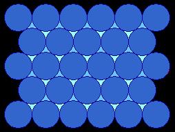


2 Crystal planes and surface modifications (100) (110) (111) bcc - body-centred cubic fcc - face-centred cubic hcp - hexagonal close packed
![Crystal planes and surface modifications Notations Square brackets, "[100]", denote a particular crystallographic direction A bar over a number denotes a negative value.](/docs-images/78/77871537/images/3-0.jpg "< > Angular brackets denote equivalent directions. ( ) denotes a particular plane or surface (hkl) where h, k and l are the Miller indexes for the plane.")
3 Crystal planes and surface modifications Notations Square brackets, "[100]", denote a particular crystallographic direction A bar over a number denotes a negative value. < > Angular brackets denote equivalent directions. ( ) denotes a particular plane or surface (hkl) where h, k and l are the Miller indexes for the plane. In a cubic system these are also the co-ordinates of the vector normal to the plane. That is, the (111) surface of an fcc crystal is normal to the [111] direction in the crystal. { } denote equivalent planes of one particular type.

4 Crystal planes and surface modifications Relaxation Relaxation is a small and subtle rearrangement of the surface layers which may nevertheless be energetically significant. It involves adjustments in the interlayer spacing perpendicular to the surface, while there is no change both for the periodicity parallel to the surface or for the surface symmetry. Unrelaxed Surface Relaxed Surface (d 1-2 < d bulk ) The driving force of relaxation is the smoothening of the electric charge density at the surface and to the formation of a surface electric field which displaces the positive outermost ionic core layer towards the bulk (Smoluchowski effect). The expansion of the third layer is due to the oscillations of the screening charge.
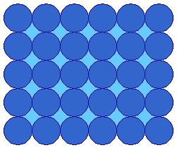
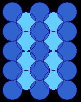
5 2D Crystallography Bravais lattices in 2D are called Bravais nets Unit cells in 2D are called unit meshes There are just 5 symmetrically different Bravais nets in 2D The centered rectangular net is the only non-primitive net
6
7 2D Crystallography: 2D Point Groups
8 2D Crystallography: 2D Space Groups The combination of the 5 Bravais nets with the 10 different point groups leads to 17 space groups in 2D (i.e. 17 surface structures) Equivalent positions, symmetry operations and long and short International notations for the 2D space groups only translation matters Translation + rotation Centered structure Translation + mirroring Translation + gliding
9 Equivalent positions, symmetry operations and long and short International notations for the 2D space groups
10 Equivalent positions, symmetry operations and long and short International notations for the 2D space groups Translation + rotation (6 fold axis) + two inequivalent mirror planes
11 2D Crystallography: Relation between Substrate and Selvage Whenever there is a selvage (clean surface or adsorbate) the surface 2D-net and 2D-mesh are referred to the substrate 2D-net and 2D-mesh The vectors c 1 and c 2 of the surface mesh may be expressed in terms of the reference net a 1 and a 2 by a matrix operation (P) c c 1 2 a P a 1 2 P P a a Since the area of the 2D substrate unit mesh is a 1 xa 2, det P is the ratio of the areas of the two meshes 11 Based on the values of det P and P ij, systems are sorted out along the following classification: 1) det P integral and all P ij integral The two meshes are simply related with the adsorbate mesh having the same translational symmetry as the whole surface 21 P P
12 2D Crystallography: Relation between Substrate and Selvage 2) det P a rational fraction (or det P integral and some P ij rational) The two meshes are rationally related. The structure is still commensurate but the true surface mesh is larger than either the substrate or adsorbate mesh. Such structures are referred to as coincidence net structures. If d 1 and d 2 are the primitive vectors of the true surface mesh, we have d d 1 2 a R a 1 2 c Q c det R and det Q are chosen to have the smallest possible integral values and: det G det R det Q 3) det P irrational The two meshes are now incommensurate and no true surface mesh exists. This might be the case if the adsorbate-adsorbate bonding is much stronger than the adsorbate-substrate bonding (e.g. rare gases) or if the adsorbed species are too large and they do not feel the periodicity of the substrate 1 2
13
14 Ricostruction and superlattices
15 2D Crystallography: Relation between Substrate and Selvage Shorthand notation (E. A. Wood, 1964) It defines the ratio of the lengths of the surface and substrate meshes along with the angle through which one mesh must be rotated to align the two pairs of primitive translation vectors. If A is the adsorbate, X the substrate material and if c 1 =p a 1 and a 2 =q c 2 with a unit mesh rotation of f, the structure is referred to as X{hkl}p x q-rf -A or often X{hkl}(p x q)rf -A Cu(100)p4mm O Cu(100)(22)-R45 -O Warning: This notation is less versatile. It is suitable for systems where the surface and substrate meshes have the same Bravais net, or where one is rectangular and the other square. It is not satisfactory for mixed symmetry meshes.
16 Structure Factor, Form Factor and Reciprocal Space The Crystalline structure is usually investigated in scattering experiments. The impinging particles are described by plane waves 0 e ikr and the scattered waves by the set of functions: j = 0 e ik R /R f j (k 0, k) e i(k-k o ) R j where f j (k 0, k) is the atomic scattering factor, determined by how the wave is reflected by the atoms within the unit cell, and e i(k-k o ) R j is the phase difference between waves reflected at the origin (zero) and at position R j For a crystal with M 1 M 2 unit cells the scattered wavefunction is obtained by summing over all scattering centers: example f(electrons) = j j j f j (k 0,k) e i(k-k o ) R j=fg The sum can be partitioned into two independent parts: the form factor F k f j exp ik r j j depending only on the internal disposition of the atoms within the unit cell (determining the scattering intensities ). The structure factor, G, determined only by the spatial arrangement of the unit cells, and giving the diffraction patterns.
17 Given R j =(n 1 a 1,n 2 a 2 ) with a 1 a 2 the unit vectors of the cell: And taking the square of the wavefunction to compute the scattering intensity we obtain the so called interference function: which has maxima for a (k-k o )=n i.e. when the momentum exchange is equal to a reciprocal lattice vector G=(2n/a 1, 2m/a 2 ) The position of the maxima in the diffraction pattern tells us about the crystal lattice symmetries, while the intensity in the different channels tells us about the atomic arrangement inside the unit cell ))] ( 2 1 [sin( ))] ( 2 1 [sin( )] ( 2 1 [sin( ))] ( 2 1 [sin( M M k k a k k a M k k a k k M a G ) ( ) ( M n M n k k a in k k a in e e G
18 In elastic scattering we have the conservation of energy (ħk) 2 /2m and of momentum p=mv=(ħk). In the scattering process we thus have: 2mE k 2 k ' Ewald Construction in 3 Dim space k ' k g hkl k 2 Energy conservation Momentum conservation where g hkl is a reciprocal lattice vector (2 indexes for 2 Dim, 3 for 3 Dim). In order diffraction to be possible k - k must be comparable or larger than g. 2 1) A vector k is drawn terminating at the origin of the reciprocal space 2) A sphere of radius k is constructed about the beginning of k 3) For any point at which the sphere passes through a reciprocal lattice point, a line to this point from the center of the sphere represents a diffracted beam k 4) Notice the reciprocal lattice vector g hkl
19 Diffraction in 2D 2 k 2 k ' k ' k g hk k 2 k 2 k ' 2 k ' 2 Conservation of Momentum Conservation of Energy k is not conserved since the translational symmetry normal to the surface is now broken The indexing of the diffracted beams is, by convention, referenced to the substrate real and reciprocal net. If the selvedge or adsorbate structures have larger periodicities, the surface reciprocal net is smaller than that of the substrate alone. The extra reciprocal net points and associated diffracted beams are denoted by fractional rather than integral indices.
 At surfaces 2D translational symmetry holds thereby only.")
20 Ewald Sphere Construction in 2D Reciprocal Space Notice that the reciprocal lattice is now replaced by infinite reciprocal lattice rods perpendicular to the surface and passing through the reciprocal net points 1) At surfaces 2D translational symmetry holds thereby only. 2) The wave vector parallel to the surface is conserved with the addition of a reciprocal net vector 3) The dashed scattered wave vectors propagate into the solid and are not observable
21 2D Crystallography: Surface Reciprocal Lattice The reciprocal net vectors A and B of the surface mesh are defined, in analogy to the 3 Dim case, as b n a A = b B = 0 A 2 a A = b B = 2π a b n The reciprocal net points of a diperiodic net may be thought of (in 3D space) as rods. The rods are infinite in extent and normal to the surface plane where they pass through the reciprocal net points. Imagine a triperiodic lattice which is expanded with no limit along one axis, thus the lattice points along this axis are moved altogether and in the limit form a rod. Example: rectangular mesh
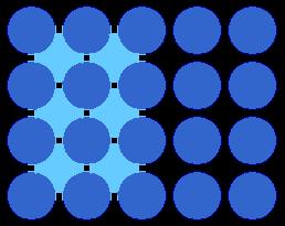
22 fcc or bcc (100) c(2x2) superlattice
23
24
25 bcc fcc
26 Relation between 3D and 2D Brillouin zones

27 Exercise: bcc -crystal
 symmetry and is therefore difficult to distinguish from the c(2x2)-h")

28 W(100) c(2x2) reconstruction Tungsten reconstructs 2x2 below 150 K. This reconstruction has c(2x2) symmetry and is therefore difficult to distinguish from the c(2x2)-h superstructure with which is was erroneously confused for a long time. Note that two domains are present. Above 150 K the surface disorders and the reconstruction is lifted so that the pattern goes back to the (1x1) determined by the underlying lattice.

29 H small coverage.. large Coverage Surface reconstructs by shifting the first W layer to the right

30 Fcc surfaces Ir(100)
 Au(111) The reconstruction")

31 Au(111) (22x3) or herringbone reconstruction Main effect : uniaxial compression Pt(100) Au(111) The reconstruction causes a 4.5% shrinking of the surface layer It occurs in 3 domains due to the 3 fold symmetry axis of the lattice

32 fcc (110) surfaces of Ir, Pt, Au
33 Diamond structure (Si, Ge) and Zinc blende (III-V) structures
34 Diamond structure: Si, Ge Jahn Teller effect Two dangling bonds per unit cell imply two surface states, one empty and one full. The pairing of the bonds and the associated lattice distortion imply a gain in energy
35 Si(001) 2x1 Si(100) non reconstructed Observed structure: Asymmetric dimers (2x1) symmetric dimers


36 Si(001) 2x1
37 Asymmetric dimers (2x1) c(4x2) and p(2x1) are nearly isoenergetic and can coexist


38 Imaging surface states by STM Scanning Tunneling microscopy gives a topographical image in real space for constant current measurements. The images depend on the tip bias and voltage sinced different states are recorded. When measuring the current vs voltage one obtains the local conductivity determined by the local density of states
39 STM: Theory Let s consider a one-dimensional barrier (we neglect the electric field at the junction and assume that the work function f is the same for both electrodes). Given a certain barrier thickness s one obtains: e 0 e 0 kz k ( sz) 2mf with k 1.1 Å -1 for f=4.5 ev 2 The matrix element is then M I 2 2m ds 2k( ) e where the sum extends over all states involved in the tunneling process 0 2 e 2ks e 0 2 represent the surface state density -I depends exponentially on barrier thickness. -For k=1.1 Å -1, I varies by one order of magnitude per Å. - High sensibility to surface corrugation ks


40 STM images of Si(001) 2x1

41 (2x1) and c(4x2) structures coexist on Ge(100) due to the energy gain associated with stress relaxation

42 Reconstruction of Si(100) and Steps Step down direction S a step more energetic than S b step

43 S b steps are rougher at non zero T
44 Si (111) (2x1) The cleaved surface exhibits a (2x1 reconstruction). The reconstruction involves displacements down to the second crystal layer Because of the Jahn Teller effect the pairing of the dimers implies a semiconducting surface.

45 Occupied surface state Empty surface state Tip bias +1V -1V
 The dots")

46 Diamond structure: Si(111) The dots correspond to electronic states on the adatoms

47 Diamond structure: Ge(111) c(2x8)
 and Wurtzite structures (two")
 and (-1,0,0)")
48 Other compounds Zincblende structure (two displaced fcc lattices 8 atoms per unit cell) and Wurtzite structures (two displaced hcp lattices 4 atoms per unit cell) (111) and (100) planes are polar and different from (-1,-1,-1) and (-1,0,0) planes.

49 III-V Semiconductors : GaAs Clivage surface : (110) Riconstruction by atom displacements within the unit cell Small changes in the bond length Ga As Covalent Bonds inclined by 27 The sp 3 bond dehybridises to a quasi sp 2 (planar geometry).


50 III-V Semiconductors : GaP basically identical to GaAs..
51
52
 charge neutralization")
53 Polar surfaces: (111) vs (-1-1-1) charge neutralization problem


54 Domain walls e.g. between fcc and hcp regions on Au(111)
55 The domain boundary: Frenkel Kontorova model chain of atoms connected by springs in a sinusoidal potential a and b are the natural lattice spacings of the chain and of the potential, respectively. Differentiating with respect to x n we obtain the equilibrium condition a Considering 0.5 ML coverage, assuming unloaded springs if the atom distance a=2b and a soft spring constant (½kb 2 << U), we get for the energy variation: when expanding for small displacements Leading to a minimum for with The displacement vanishes indeed when k tends to zero and the associated energy reads: 2
56 In the limit of strong springs the overlayer becomes incommensurate, but in the limit of displacements u nearly uniform from one atom to the next gives the sine Gordon equation in which u n+1 +u n-1-2u n reduces to the second derivative of the continuous function u(n) Which may be solved by multiplying by du/dn and by partial integration K=U/k in the limit of u(n)0 Domain wall width 4r Integrating again yields


57 Stereogram of bcc and fcc surfaces achiral chiral
58 Steps and defects
59

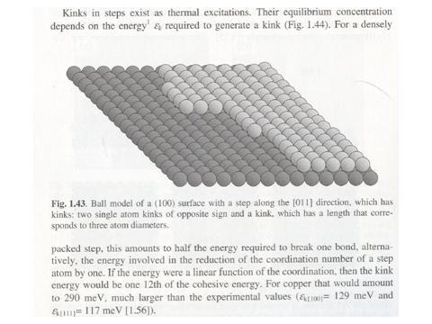
60 Kinks at steps For Cu with α=0.3 one obtains ε=134 mev/kink in fair agreement with experiment
61 Interfaces

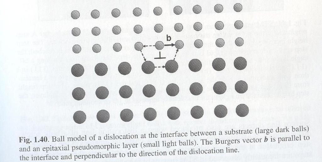
62 Dislocations Notice: at the dislocation the steps are straight
63
64
2. Diffraction as a means to determine crystal structure
 2. Diffraction as a means to determine crystal structure Recall de Broglie matter waves: He atoms: [E (ev)] 1/2 = 0.14 / (Å) E 1Å = 0.0196 ev Neutrons: [E (ev)] 1/2 = 0.28 / (Å) E 1Å = 0.0784 ev Electrons:
disordered, ordered and coherent with the substrate, and ordered but incoherent with the substrate.
 5. Nomenclature of overlayer structures Thus far, we have been discussing an ideal surface, which is in effect the structure of the topmost substrate layer. The surface (selvedge) layers of the solid however
2. Diffraction as a means to determine crystal structure
 Page 1 of 22 2. Diffraction as a means to determine crystal structure Recall de Broglie matter waves: 2 p h E = where p = 2m λ h 1 E = ( ) 2m λ hc E = hυ = ( photons) λ ( matter wave) He atoms: [E (ev)]
Bulk Structures of Crystals
 Bulk Structures of Crystals 7 crystal systems can be further subdivided into 32 crystal classes... see Simon Garrett, "Introduction to Surface Analysis CEM924": http://www.cem.msu.edu/~cem924sg/lecturenotes.html
2. Surface geometric and electronic structure: a primer
 2. Surface geometric and electronic structure: a primer 2.1 Surface crystallography 2.1.1. Crystal structures - A crystal structure is made up of two basic elements: lattice + basis Basis: Lattice: simplest
Structure of Surfaces
 Structure of Surfaces C Stepped surface Interference of two waves Bragg s law Path difference = AB+BC =2dsin ( =glancing angle) If, n =2dsin, constructive interference Ex) in a cubic lattice of unit cell
Properties of Individual Nanoparticles
 TIGP Introduction technology (I) October 15, 2007 Properties of Individual Nanoparticles Clusters 1. Very small -- difficult to image individual nanoparticles. 2. New physical and/or chemical properties
STM spectroscopy (STS)
") STM spectroscopy (STS) di dv 4 e ( E ev, r) ( E ) M S F T F Basic concepts of STS. With the feedback circuit open the variation of the tunneling current due to the application of a small oscillating voltage
STM spectroscopy (STS) di dv 4 e ( E ev, r) ( E ) M S F T F Basic concepts of STS. With the feedback circuit open the variation of the tunneling current due to the application of a small oscillating voltage
Surface physics, Bravais lattice
 Surface physics, Bravais lattice 1. Structure of the solid surface characterized by the (Bravais) lattice + space + point group lattice describes also the symmetry of the solid material vector directions
2) Atom manipulation. Xe / Ni(110) Model: Experiment:
 Atom manipulation. Xe / Ni(110) Model: Experiment:") 2) Atom manipulation D. Eigler & E. Schweizer, Nature 344, 524 (1990) Xe / Ni(110) Model: Experiment: G.Meyer, et al. Applied Physics A 68, 125 (1999) First the tip is approached close to the adsorbate
2) Atom manipulation D. Eigler & E. Schweizer, Nature 344, 524 (1990) Xe / Ni(110) Model: Experiment: G.Meyer, et al. Applied Physics A 68, 125 (1999) First the tip is approached close to the adsorbate
Introduction to Solid State Physics or the study of physical properties of matter in a solid phase
 Introduction to Solid State Physics or the study of physical properties of matter in a solid phase Prof. Germar Hoffmann 1. Crystal Structures 2. Reciprocal Lattice 3. Crystal Binding and Elastic Constants
Scanning Tunneling Microscopy. how does STM work? the quantum mechanical picture example of images how can we understand what we see?
 Scanning Tunneling Microscopy how does STM work? the quantum mechanical picture example of images how can we understand what we see? Observation of adatom diffusion with a field ion microscope Scanning
Surface and Interface Science Physics 627; Chemistry 542. Lectures 3 Feb 1, Surface Structure
 Surface and Interface Science Physics 67; Chemistry 54 Lectures 3 Fe, 03 Surface Structure References: ) Zangwill, Pp. 8-3 ) Woodruff & Delchar, Chapter 3) Masel, Chapter 4) Ertl & Kuppers, 0-07 5) Luth,
Crystal Structure. Dr Bindu Krishnan
 Solid State Physics-1 Crystal Structure Dr Bindu Krishnan CRYSTAL LATTICE What is crystal (space) lattice? In crystallography, only the geometrical properties of the crystal are of interest, therefore
The Solid State. Phase diagrams Crystals and symmetry Unit cells and packing Types of solid
 The Solid State Phase diagrams Crystals and symmetry Unit cells and packing Types of solid Learning objectives Apply phase diagrams to prediction of phase behaviour Describe distinguishing features of
Chem 728 Introduction to Solid Surfaces
 Chem 728 Introduction to Solid Surfaces Solids: hard; fracture; not compressible; molecules close to each other Liquids: molecules mobile, but quite close to each other Gases: molecules very mobile; compressible
Crystals Statics. Structural Properties. Geometry of lattices. Aug 23, 2018
 Crystals Statics. Structural Properties. Geometry of lattices Aug 23, 2018 Crystals Why (among all condensed phases - liquids, gases) look at crystals? We can take advantage of the translational symmetry,
Quantum Condensed Matter Physics Lecture 5
 Quantum Condensed Matter Physics Lecture 5 detector sample X-ray source monochromator David Ritchie http://www.sp.phy.cam.ac.uk/drp2/home QCMP Lent/Easter 2019 5.1 Quantum Condensed Matter Physics 1. Classical
UNIT I SOLID STATE PHYSICS
 UNIT I SOLID STATE PHYSICS CHAPTER 1 CRYSTAL STRUCTURE 1.1 INTRODUCTION When two atoms are brought together, two kinds of forces: attraction and repulsion come into play. The force of attraction increases
The Hamiltonian. 2.1 The Schrödinger Equation
 2 The Hamiltonian Any theoretical description has to start with the definition of the system under consideration and a determination of the fundamental interactions present in the system. This information
Concepts in Surface Physics
 M.-C. Desjonqueres D. Spanjaard Concepts in Surface Physics Second Edition With 257 Figures Springer 1. Introduction................................. 1 2. Thermodynamical and Statistical Properties of
Crystallographic structure Physical vs Chemical bonding in solids
 Crystallographic structure Physical vs Chemical bonding in solids Inert gas and molecular crystals: Van der Waals forces (physics) Water and organic chemistry H bonds (physics) Quartz crystal SiO 2 : covalent
Introductory Nanotechnology ~ Basic Condensed Matter Physics ~
 Introductory Nanotechnology ~ Basic Condensed Matter Physics ~ Atsufumi Hirohata Department of Electronics Go into Nano-Scale Lateral Size [m] 10-3 10-6 Micron-scale Sub-Micron-scale Nano-scale Human hair
Phys 460 Describing and Classifying Crystal Lattices
 Phys 460 Describing and Classifying Crystal Lattices What is a material? ^ crystalline Regular lattice of atoms Each atom has a positively charged nucleus surrounded by negative electrons Electrons are
Electronic Structure Theory for Periodic Systems: The Concepts. Christian Ratsch
 Electronic Structure Theory for Periodic Systems: The Concepts Christian Ratsch Institute for Pure and Applied Mathematics and Department of Mathematics, UCLA Motivation There are 10 20 atoms in 1 mm 3
1.4 Crystal structure
 1.4 Crystal structure (a) crystalline vs. (b) amorphous configurations short and long range order only short range order Abbildungen: S. Hunklinger, Festkörperphysik, Oldenbourg Verlag represenatives of
Structure and Dynamics : An Atomic View of Materials
 Structure and Dynamics : An Atomic View of Materials MARTIN T. DOVE Department ofearth Sciences University of Cambridge OXFORD UNIVERSITY PRESS Contents 1 Introduction 1 1.1 Observations 1 1.1.1 Microscopic
Surface Sensitivity & Surface Specificity
 Surface Sensitivity & Surface Specificity The problems of sensitivity and detection limits are common to all forms of spectroscopy. In its simplest form, the question of sensitivity boils down to whether
Phys 412 Solid State Physics. Lecturer: Réka Albert
 Phys 412 Solid State Physics Lecturer: Réka Albert What is a solid? A material that keeps its shape Can be deformed by stress Returns to original shape if it is not strained too much Solid structure
Basics of DFT applications to solids and surfaces
 Basics of DFT applications to solids and surfaces Peter Kratzer Physics Department, University Duisburg-Essen, Duisburg, Germany E-mail: Peter.Kratzer@uni-duisburg-essen.de Periodicity in real space and
We need to be able to describe planes and directions.
 We need to be able to describe planes and directions. Miller Indices & XRD 1 2 Determining crystal structure and identifying materials (B) Plastic deformation Plastic deformation and mechanical properties
Experimental methods in physics. Local probe microscopies I
 Experimental methods in physics Local probe microscopies I Scanning tunnelling microscopy (STM) Jean-Marc Bonard Academic year 09-10 1. Scanning Tunneling Microscopy 1.1. Introduction Image of surface
Encyclopedia of Applied Physics. Surfaces and Interfaces of Solids, Structure of
 i Preface Encyclopedia of Applied Physics Feng Liu, M. Hohage, and M. G. Lagally University of Wisconsin-Madison, Madison, WI 53706 This encyclopedia article gives an overview of basic concepts and fundamental
* motif: a single or repeated design or color
 Chapter 2. Structure A. Electronic structure vs. Geometric structure B. Clean surface vs. Adsorbate covered surface (substrate + overlayer) C. Adsorbate structure - how are the adsorbed molecules bound
Structure analysis: Electron diffraction LEED TEM RHEED
 Structure analysis: Electron diffraction LEED: Low Energy Electron Diffraction SPA-LEED: Spot Profile Analysis Low Energy Electron diffraction RHEED: Reflection High Energy Electron Diffraction TEM: Transmission
Cross-Section Scanning Tunneling Microscopy of InAs/GaSb Superlattices
 Cross-Section Scanning Tunneling Microscopy of InAs/GaSb Superlattices Cecile Saguy A. Raanan, E. Alagem and R. Brener Solid State Institute. Technion, Israel Institute of Technology, Haifa 32000.Israel
The structure of liquids and glasses. The lattice and unit cell in 1D. The structure of crystalline materials. Describing condensed phase structures
 Describing condensed phase structures Describing the structure of an isolated small molecule is easy to do Just specify the bond distances and angles How do we describe the structure of a condensed phase?
Physics 211B : Problem Set #0
 Physics 211B : Problem Set #0 These problems provide a cross section of the sort of exercises I would have assigned had I taught 211A. Please take a look at all the problems, and turn in problems 1, 4,
Symmetry Crystallography
 Crystallography Motif: the fundamental part of a symmetric design that, when repeated, creates the whole pattern In 3-D, translation defines operations which move the motif into infinitely repeating patterns
SOLID STATE 18. Reciprocal Space
 SOLID STATE 8 Reciprocal Space Wave vectors and the concept of K-space can simplify the explanation of several properties of the solid state. They will be introduced to provide more information on diffraction
Geometry of Crystal Lattice
 0 Geometry of Crystal Lattice 0.1 Translational Symmetry The crystalline state of substances is different from other states (gaseous, liquid, amorphous) in that the atoms are in an ordered and symmetrical
Nearly Free Electron Gas model - I
 Nearly Free Electron Gas model - I Contents 1 Free electron gas model summary 1 2 Electron effective mass 3 2.1 FEG model for sodium...................... 4 3 Nearly free electron model 5 3.1 Primitive
Imaging Methods: Scanning Force Microscopy (SFM / AFM)
") Imaging Methods: Scanning Force Microscopy (SFM / AFM) The atomic force microscope (AFM) probes the surface of a sample with a sharp tip, a couple of microns long and often less than 100 Å in diameter.
Imaging Methods: Scanning Force Microscopy (SFM / AFM) The atomic force microscope (AFM) probes the surface of a sample with a sharp tip, a couple of microns long and often less than 100 Å in diameter.
Introduction to Crystal Structure and Bonding. Prof.P. Ravindran, Department of Physics, Central University of Tamil Nadu, India
 Introduction to Crystal Structure and Bonding 1 Prof.P. Ravindran, Department of Physics, Central University of Tamil Nadu, India http://folk.uio.no/ravi/semi2013 Fundamental Properties of matter 2 Matter:
CHEM-E5225 :Electron Microscopy. Diffraction 1
 CHEM-E5225 :Electron Microscopy Diffraction 1 2018-10-15 Yanling Ge Text book: Transmission electron microscopy by David B Williams & C. Barry Carter. 2009, Springer Outline Diffraction in TEM Thinking
Physics 541: Condensed Matter Physics
 Physics 541: Condensed Matter Physics Final Exam Monday, December 17, 2012 / 14:00 17:00 / CCIS 4-285 Student s Name: Instructions There are 24 questions. You should attempt all of them. Mark your response
FIRST MIDTERM EXAM Chemistry March 2011 Professor Buhro
 FIRST MIDTERM EXAM Chemistry 465 1 March 2011 Professor Buhro Signature Print Name Clearly ID Number: Information. This is a closed-book exam; no books, notes, other students, other student exams, or any
M2 TP. Low-Energy Electron Diffraction (LEED)
") M2 TP Low-Energy Electron Diffraction (LEED) Guide for report preparation I. Introduction: Elastic scattering or diffraction of electrons is the standard technique in surface science for obtaining structural
M2 TP Low-Energy Electron Diffraction (LEED) Guide for report preparation I. Introduction: Elastic scattering or diffraction of electrons is the standard technique in surface science for obtaining structural
Introduction to crystallography The unitcell The resiprocal space and unitcell Braggs law Structure factor F hkl and atomic scattering factor f zθ
 Introduction to crystallography The unitcell The resiprocal space and unitcell Braggs law Structure factor F hkl and atomic scattering factor f zθ Introduction to crystallography We divide materials into
4. Interpenetrating simple cubic
 2 1. The correct structure t of CsClCl crystal is 1. Simple cubic 2. Body centered cubic 3. Face centered cubic 4. Interpenetrating simple cubic If corner as well as the particle at the center are same
Crystal planes. Neutrons: magnetic moment - interacts with magnetic materials or nuclei of non-magnetic materials. (in Å)
") Crystallography: neutron, electron, and X-ray scattering from periodic lattice, scattering of waves by periodic structures, Miller indices, reciprocal space, Ewald construction. Diffraction: Specular,
Crystallography: neutron, electron, and X-ray scattering from periodic lattice, scattering of waves by periodic structures, Miller indices, reciprocal space, Ewald construction. Diffraction: Specular,
SOLID STATE PHYSICS. Second Edition. John Wiley & Sons. J. R. Hook H. E. Hall. Department of Physics, University of Manchester
 SOLID STATE PHYSICS Second Edition J. R. Hook H. E. Hall Department of Physics, University of Manchester John Wiley & Sons CHICHESTER NEW YORK BRISBANE TORONTO SINGAPORE Contents Flow diagram Inside front
Atomic Arrangement. Primer in Materials Spring
 Atomic Arrangement Primer in Materials Spring 2017 30.4.2017 1 Levels of atomic arrangements No order In gases, for example the atoms have no order, they are randomly distributed filling the volume to
PART 1 Introduction to Theory of Solids
 Elsevier UK Job code: MIOC Ch01-I044647 9-3-2007 3:03p.m. Page:1 Trim:165 240MM TS: Integra, India PART 1 Introduction to Theory of Solids Elsevier UK Job code: MIOC Ch01-I044647 9-3-2007 3:03p.m. Page:2
Heterostructures and sub-bands
 Heterostructures and sub-bands (Read Datta 6.1, 6.2; Davies 4.1-4.5) Quantum Wells In a quantum well, electrons are confined in one of three dimensions to exist within a region of length L z. If the barriers
Solids. properties & structure
 Solids properties & structure Determining Crystal Structure crystalline solids have a very regular geometric arrangement of their particles the arrangement of the particles and distances between them is
Solid State Physics 460- Lecture 5 Diffraction and the Reciprocal Lattice Continued (Kittel Ch. 2)
") Solid State Physics 460- Lecture 5 Diffraction and the Reciprocal Lattice Continued (Kittel Ch. 2) Ewald Construction 2θ k out k in G Physics 460 F 2006 Lect 5 1 Recall from previous lectures Definition
Solid State Physics 460- Lecture 5 Diffraction and the Reciprocal Lattice Continued (Kittel Ch. 2) Ewald Construction 2θ k out k in G Physics 460 F 2006 Lect 5 1 Recall from previous lectures Definition
Keble College - Hilary 2012 Section VI: Condensed matter physics Tutorial 2 - Lattices and scattering
 Tomi Johnson Keble College - Hilary 2012 Section VI: Condensed matter physics Tutorial 2 - Lattices and scattering Please leave your work in the Clarendon laboratory s J pigeon hole by 5pm on Monday of
Physical Chemistry I. Crystal Structure
 Physical Chemistry I Crystal Structure Crystal Structure Introduction Crystal Lattice Bravis Lattices Crytal Planes, Miller indices Distances between planes Diffraction patters Bragg s law X-ray radiation
Lecture 2. Unit Cells and Miller Indexes. Reading: (Cont d) Anderson 2 1.8,
 Anderson 2 1.8,") Lecture 2 Unit Cells and Miller Indexes Reading: (Cont d) Anderson 2 1.8, 2.1-2.7 Unit Cell Concept The crystal lattice consists of a periodic array of atoms. Unit Cell Concept A building block that can
Lecture 2 Unit Cells and Miller Indexes Reading: (Cont d) Anderson 2 1.8, 2.1-2.7 Unit Cell Concept The crystal lattice consists of a periodic array of atoms. Unit Cell Concept A building block that can
3.012 Structure An Introduction to X-ray Diffraction
 3.012 Structure An Introduction to X-ray Diffraction This handout summarizes some topics that are important for understanding x-ray diffraction. The following references provide a thorough explanation
Supplementary Figure 1 Experimental setup for crystal growth. Schematic drawing of the experimental setup for C 8 -BTBT crystal growth.
 Supplementary Figure 1 Experimental setup for crystal growth. Schematic drawing of the experimental setup for C 8 -BTBT crystal growth. Supplementary Figure 2 AFM study of the C 8 -BTBT crystal growth
Quantum Condensed Matter Physics Lecture 4
 Quantum Condensed Matter Physics Lecture 4 David Ritchie QCMP Lent/Easter 2019 http://www.sp.phy.cam.ac.uk/drp2/home 4.1 Quantum Condensed Matter Physics 1. Classical and Semi-classical models for electrons
Materials for Civil and Construction Engineers CHAPTER 2. Nature of Materials
 Materials for Civil and Construction Engineers CHAPTER 2 Nature of Materials Bonds 1. Primary Bond: forms when atoms interchange or share electrons in order to fill the outer (valence) shells like noble
Survey of structural and electronic properties of C60 on close-packed metal surfaces
 Hong Kong Baptist University From the SelectedWorks of Professor Michel Andre Van Hove 2012 Survey of structural and electronic properties of C60 on close-packed metal surfaces Xing-Qiang Shi, Department
Class 29: Reciprocal Space 3: Ewald sphere, Simple Cubic, FCC and BCC in Reciprocal Space
 Class 29: Reciprocal Space 3: Ewald sphere, Simple Cubic, FCC and BCC in Reciprocal Space We have seen that diffraction occurs when, in reciprocal space, Let us now plot this information. Let us designate
Lecture 6 - Bonding in Crystals
 Lecture 6 onding in Crystals inding in Crystals (Kittel Ch. 3) inding of atoms to form crystals A crystal is a repeated array of atoms Why do they form? What are characteristic bonding mechanisms? How
... 3, , = a (1) 3 3 a 2 = a (2) The reciprocal lattice vectors are defined by the condition a b = 2πδ ij, which gives
 3 3 a 2 = a (2) The reciprocal lattice vectors are defined by the condition a b = 2πδ ij, which gives") PHZ646: Fall 013 Problem set # 4: Crystal Structure due Monday, 10/14 at the time of the class Instructor: D. L. Maslov maslov@phys.ufl.edu 39-0513 Rm. 114 Office hours: TR 3 pm-4 pm Please help your instructor
PHZ646: Fall 013 Problem set # 4: Crystal Structure due Monday, 10/14 at the time of the class Instructor: D. L. Maslov maslov@phys.ufl.edu 39-0513 Rm. 114 Office hours: TR 3 pm-4 pm Please help your instructor
Surface Characte i r i zat on LEED Photoemission Phot Linear optics
 Surface Characterization i LEED Photoemission Linear optics Surface characterization with electrons MPS M.P. Seah, WA W.A. Dench, Surf. Interf. Anal. 1 (1979) 2 LEED low energy electron diffraction De
Classification of Solids, Fermi Level and Conductivity in Metals Dr. Anurag Srivastava
 Classification of Solids, Fermi Level and Conductivity in Metals Dr. Anurag Srivastava Web address: http://tiiciiitm.com/profanurag Email: profanurag@gmail.com Visit me: Room-110, Block-E, IIITM Campus
Scanning Tunneling Microscopy (STM)
") Page 1 of 8 Scanning Tunneling Microscopy (STM) This is the fastest growing surface analytical technique, which is replacing LEED as the surface imaging tool (certainly in UHV, air and liquid). STM has
Page 1 of 8 Scanning Tunneling Microscopy (STM) This is the fastest growing surface analytical technique, which is replacing LEED as the surface imaging tool (certainly in UHV, air and liquid). STM has
tip of a current tip and the sample. Components: 3. Coarse sample-to-tip isolation system, and
 SCANNING TUNNELING MICROSCOPE Brief history: Heinrich Rohrer and Gerd K. Binnig, scientists at IBM's Zurich Research Laboratory in Switzerland, are awarded the 1986 Nobel Prize in physicss for their work
ECE 474: Principles of Electronic Devices. Prof. Virginia Ayres Electrical & Computer Engineering Michigan State University
 ECE 474: Principles of Electronic Devices Prof. Virginia Ayres Electrical & Computer Engineering Michigan State University ayresv@msu.edu Lecture 06: Completed: Chapter 01: quantify physical structures
SECOND PUBLIC EXAMINATION. Honour School of Physics Part C: 4 Year Course. Honour School of Physics and Philosophy Part C C3: CONDENSED MATTER PHYSICS
 A11046W1 SECOND PUBLIC EXAMINATION Honour School of Physics Part C: 4 Year Course Honour School of Physics and Philosophy Part C C3: CONDENSED MATTER PHYSICS TRINITY TERM 2015 Wednesday, 17 June, 2.30
2 Symmetry. 2.1 Structure of carbon nanotubes
 2 Symmetry Carbon nanotubes are hollow cylinders of graphite sheets. They can be viewed as single molecules, regarding their small size ( nm in diameter and µm length), or as quasi-one dimensional crystals
Graphite, graphene and relativistic electrons
 Graphite, graphene and relativistic electrons Introduction Physics of E. graphene Y. Andrei Experiments Rutgers University Transport electric field effect Quantum Hall Effect chiral fermions STM Dirac
3.012 PS Issued: Fall 2003 Graded problems due:
 3.012 PS 4 3.012 Issued: 10.07.03 Fall 2003 Graded problems due: 10.15.03 Graded problems: 1. Planes and directions. Consider a 2-dimensional lattice defined by translations T 1 and T 2. a. Is the direction
Atomic and electronic structures of Si(111)-( 3x 3)R30 o -Au and (6x6)-Au surfaces
-( 3x 3)R30 o -Au and (6x6)-Au surfaces") Atomic and electronic structures of Si(111)-( 3x 3)R30 o -Au and (6x6)-Au surfaces C. H. Patterson School of Physics, Trinity College Dublin, Dublin 2, Ireland (Dated: June 13, 2015) Si(111)-Au surfaces
Atomic and electronic structures of Si(111)-( 3x 3)R30 o -Au and (6x6)-Au surfaces C. H. Patterson School of Physics, Trinity College Dublin, Dublin 2, Ireland (Dated: June 13, 2015) Si(111)-Au surfaces
Ionic Bonding. Chem
 Whereas the term covalent implies sharing of electrons between atoms, the term ionic indicates that electrons are taken from one atom by another. The nature of ionic bonding is very different than that
1 Review of semiconductor materials and physics
 Part One Devices 1 Review of semiconductor materials and physics 1.1 Executive summary Semiconductor devices are fabricated using specific materials that offer the desired physical properties. There are
Introduction to Condensed Matter Physics
 Introduction to Condensed Matter Physics Crystalline Solids - Introduction M.P. Vaughan Overview Overview of course Crystal solids Crystal structure Crystal symmetry The reciprocal lattice Band theory
Tensor-LEED Analysis of Oxide Surfaces
 Chapter 6 Tensor-LEED Analysis of xide Surfaces 6.1 The Ag(100) Surface 6.1.1 Introduction The use of LEED as a technique for surface structural determination began with the study of clean surfaces. Low
Physics of Materials: Classification of Solids On The basis of Geometry and Bonding (Intermolecular forces)
") Physics of Materials: Classification of Solids On The basis of Geometry and Bonding (Intermolecular forces) Dr. Anurag Srivastava Atal Bihari Vajpayee Indian Institute of Information Technology and Manegement,
Physics of Materials: Classification of Solids On The basis of Geometry and Bonding (Intermolecular forces) Dr. Anurag Srivastava Atal Bihari Vajpayee Indian Institute of Information Technology and Manegement,
Electronic Properties of Ultimate Nanowires. F. J. Himpsel, S. C. Erwin, I. Barke,
 Electronic Properties of Ultimate Nanowires F. J. Himpsel, S. C. Erwin, I. Barke, Nanostructures with Atomic Precision Single-Atom Wire, Single Wave Function Ultimate Limits of Electronics, Data Storage
Lecture 8 January 24, 2013 GaAs crystal surfaces, n-p dopants Si
 Lecture 8 January 24, 2013 Ga crystal surfaces, n-p dopants Si Nature of the Chemical Bond with applications to catalysis, materials science, nanotechnology, surface science, bioinornic chemistry, and
Energy Spectroscopy. Ex.: Fe/MgO
 Energy Spectroscopy Spectroscopy gives access to the electronic properties (and thus chemistry, magnetism,..) of the investigated system with thickness dependence Ex.: Fe/MgO Fe O Mg Control of the oxidation
3.091 Introduction to Solid State Chemistry. Lecture Notes No. 5a ELASTIC BEHAVIOR OF SOLIDS
 3.091 Introduction to Solid State Chemistry Lecture Notes No. 5a ELASTIC BEHAVIOR OF SOLIDS 1. INTRODUCTION Crystals are held together by interatomic or intermolecular bonds. The bonds can be covalent,
Crystallographic Symmetry. Jeremy Karl Cockcroft
 Crystallographic Symmetry Jeremy Karl Cockcroft Why bother? To describe crystal structures Simplifies the description, e.g. NaCl structure Requires coordinates for just 2 atoms + space group symmetry!
Energy Spectroscopy. Excitation by means of a probe
 Energy Spectroscopy Excitation by means of a probe Energy spectral analysis of the in coming particles -> XAS or Energy spectral analysis of the out coming particles Different probes are possible: Auger
1 Crystal Structures. of three-dimensional crystals. Here we use two-dimensional examples to illustrate the concepts.
 3 1 Crystal Structures A crystal is a periodic array of atoms. Many elements and quite a few compounds are crystalline at low enough temperatures, and many of the solid materials in our everyday life (like
1/2, 1/2,1/2, is the center of a cube. Induces of lattice directions and crystal planes (a) Directions in a crystal Directions in a crystal are
 Directions in a crystal Directions in a crystal are") Crystallography Many materials in nature occur as crystals. Examples include the metallic elements gold, copper and silver, ionic compounds such as salt (e.s. NaCl); ceramics, rutile TiO2; and nonmetallic
Crystallography Many materials in nature occur as crystals. Examples include the metallic elements gold, copper and silver, ionic compounds such as salt (e.s. NaCl); ceramics, rutile TiO2; and nonmetallic
Semiconductor physics I. The Crystal Structure of Solids
 Lecture 3 Semiconductor physics I The Crystal Structure of Solids 1 Semiconductor materials Types of solids Space lattices Atomic Bonding Imperfection and doping in SOLIDS 2 Semiconductor Semiconductors
Lecture 8 January 28, Silicon crystal surfaces
 Lecture 8 January 28, 203 Nature of the Chemical Bond with applications to catalysis, materials science, nanotechnology, surface science, bioinorganic chemistry, and energy Course number: Ch20a Hours:
Spins and spin-orbit coupling in semiconductors, metals, and nanostructures
 B. Halperin Spin lecture 1 Spins and spin-orbit coupling in semiconductors, metals, and nanostructures Behavior of non-equilibrium spin populations. Spin relaxation and spin transport. How does one produce
Atomic Arrangement. Primer Materials For Science Teaching Spring
 Atomic Arrangement Primer Materials For Science Teaching Spring 2016 31.3.2015 Levels of atomic arrangements No order In gases, for example the atoms have no order, they are randomly distributed filling
S.No. Crystalline Solids Amorphous solids 1 Regular internal arrangement of irregular internal arrangement of particles
 Classification of solids: Crystalline and Amorphous solids: S.No. Crystalline Solids Amorphous solids 1 Regular internal arrangement of irregular internal arrangement of particles particles 2 Sharp melting
Chapter 4: Bonding in Solids and Electronic Properties. Free electron theory
 Chapter 4: Bonding in Solids and Electronic Properties Free electron theory Consider free electrons in a metal an electron gas. regards a metal as a box in which electrons are free to move. assumes nuclei
3. SCANNING TUNNELING MICROSCOPY Electronic Tunneling JIN-FENG JIA, WEI-SHENG YANG, AND QI-KUN XUE
 3. SCANNING TUNNELING MICROSCOPY JIN-FENG JIA, WEI-SHENG YANG, AND QI-KUN XUE 1. BASIC PRINCIPLES OF SCANNING TUNNELING MICROSCOPY In spite of its conceptually simple operation principle, scanning tunneling
Chapter 2. Theoretical background. 2.1 Itinerant ferromagnets and antiferromagnets
 Chapter 2 Theoretical background The first part of this chapter gives an overview of the main static magnetic behavior of itinerant ferromagnetic and antiferromagnetic materials. The formation of the magnetic
Solid Surfaces, Interfaces and Thin Films
 Hans Lüth Solid Surfaces, Interfaces and Thin Films Fifth Edition With 427 Figures.2e Springer Contents 1 Surface and Interface Physics: Its Definition and Importance... 1 Panel I: Ultrahigh Vacuum (UHV)