Density-Dependent Electron Transport and Precise Modeling of GaN HEMTs
|
|
|
- Sharyl Barnett
- 6 years ago
- Views:
Transcription
1 Density-Dependent Electron Transport and Precise Modeling of GaN HEMTs Sanyam Bajaj 1,a), Omor F. Shoron 1, Pil Sung Park 1, Sriram Krishnamoorthy 1, Fatih Akyol 1, Ting-Hsiang Hung 1, Shahed Reza 2, Eduardo M. Chumbes 2, Jacob Khurgin 3 and Siddharth Rajan 1 1 Department of Electrical & Computer Engineering, The Ohio State University, Columbus, OH Raytheon Integrated Defense Systems, Andover, MA Department of Electrical & Computer Engineering, Johns Hopkins University, Baltimore, MD Department of Material Science & Engineering, The Ohio State University, Columbus, OH Keywords: GaN HEMT, electron velocity, 2DEG velocity, density dependent velocity, electron transport, TCAD modeling GaN, TCAD simulation GaN Abstract: We report on the direct measurement of two-dimensional sheet charge density dependence of electron transport in AlGaN/GaN high electron mobility transistors. Pulsed IV measurements established increasing electron velocities with decreasing sheet charge densities, resulting in saturation velocity of 1.9 x 10 7 cm/s at a low sheet charge density of 7.8 x cm -2. A new optical phonon emission-based electron velocity model for GaN is also presented. It accommodates stimulated LO phonon emission which clamps the electron velocity with strong electron-phonon interaction and long LO phonon lifetime in GaN. A comparison with the measured density-dependent saturation velocity shows that it captures the dependence rather well. Finally, the experimental result is applied in TCAD-based device simulator to predict DC and small signal characteristics of a reported GaN HEMT. Good agreement between the simulated and reported experimental results validated the measurement presented in this report and established accurate modeling of GaN HEMTs. a) Author to whom correspondence should be addressed. Electronic mail: bajaj.10@osu.edu Tel:
2 III-nitride high electron mobility transistors (HEMTs) have demonstrated promising high frequency operation for RF power amplifying applications 1-4. Their high current and power gain capability, and further increases in the operation frequency could enable high power electronics in the mm-wave and THz regime. The intrinsic current unity gain cutoff frequency (ft,intrinsic) is directly proportional to the electron velocity in the channel. While parasitics do play an important role in the frequency performance, recent advances in ohmic contact technology have achieved ultra-low resistance 2,5,6 (< 0.1 Ω.mm), thereby making the channel transit delay the main component of the overall delay in GaN HEMTs. Monte Carlo simulations in GaN have predicted peak electron drift velocities as high as 3 x 10 7 cm/s, with comparatively lower saturation velocities up to ~ 2 x 10 7 cm/s, limited mainly by optical phonon scattering From the total time delay analysis in recent ultra-scaled GaN HEMT results, the average electron velocity, vave, of the devices was found to be in the range from to cm/s 1-4. Most reports of GaN HEMT RF performance report the peak cutoff frequency, which is typically observed at 10-20% of the highest saturated current density. The current gain, however, is found to drop significantly as the current density is increased. The transconductance profile in GaN HEMTs also shows a similar trend. For applications of GaN HEMTs in power amplifiers, where large signal gain and linearity are critical, the current and power gain values over the entire operating range are important. The reason for this reduction in current gain and transconductance as a function of channel charge density was investigated theoretically and shown to be directly related to the charge-dependent channel velocity 12. In this report, we directly measure two-dimensional sheet density (ns)-dependent electron velocity in AlGaN/GaN HEMTs at room temperature. A new carrier transport model based on the strong interaction between optical phonons and electron carriers in GaN HEMTs is also presented. Finally, the measured sheet density dependence of electron transport in two-dimensional electron gases (2DEGs) is 2
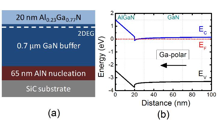
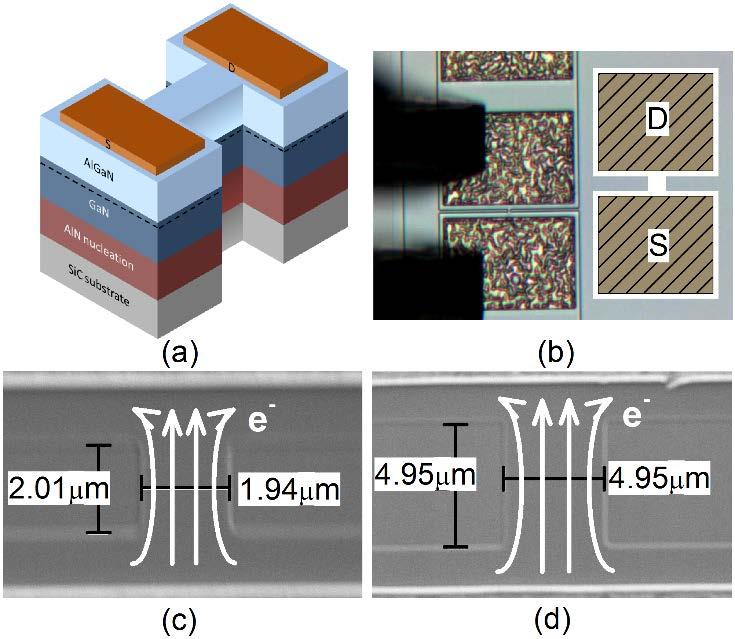
3 applied in TCAD simulation of DC and RF characteristics of a reported GaN HEMT and compared to the experimental results. HEMT structures (20 nm Al0.23Ga0.77N/GaN) shown in Figure 1, grown on SiC substrates by plasma-assisted molecular beam epitaxy (PAMBE) 13 were used for this study. I-shaped test structure consisting of wide contact/access regions and a thin constriction defined by mesa isolation (of depth 100 nm) was used to investigate the velocity field characteristics (Figure 2). Due to the geometry of this device, the resistance from the ohmic/access regions is significantly lower (at least 14X) than that from the constriction 14,15. Therefore it can be assumed that entire potential drop and current limiting mechanisms are related to the constriction. The velocity ve was estimated from the current density J ( v = e J qn S ) as a function of sheet charge density (ns), where q is the electronic charge. The sheet charge density was estimated by Hall measurements made on van der Pauw patterns. Since the resistance of the constriction is estimated to be significantly higher than the ohmic/access regions, the field F across a constriction of length d was assumed to be given by V F = d, where V is the applied bias. To measure velocity at varying electron concentrations, the constriction region was recess etched to different depths while the access regions were left unetched to maintain a low access resistance. All measurements were done at room temperature. The fabrication of the test structures was done as follows. Ti/Al/Ni/Au ohmic contacts (100 μm wide) were deposited by e-beam evaporation and alloyed through rapid thermal annealing for 30 seconds at 850 C in N2 ambient. Cl2/BCl3 plasma-based dry etching (RIE power of ~ 10 Watts) was used to define isolation mesas. For velocity measurements, I-shaped test structures of width 2 μm, 5 μm and 10 μm, and length 0.7 μm, 1 μm and 2 μm were used. The constriction dimensions were inspected 3
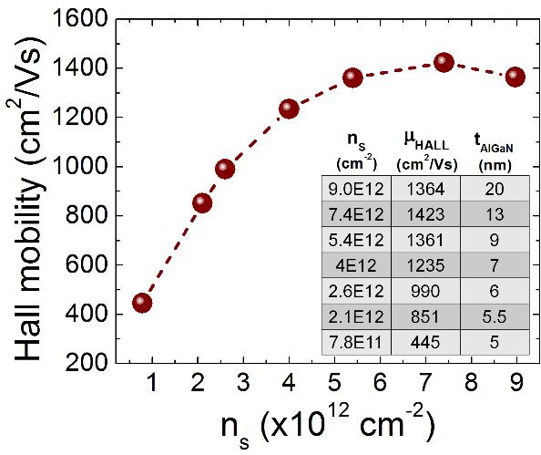
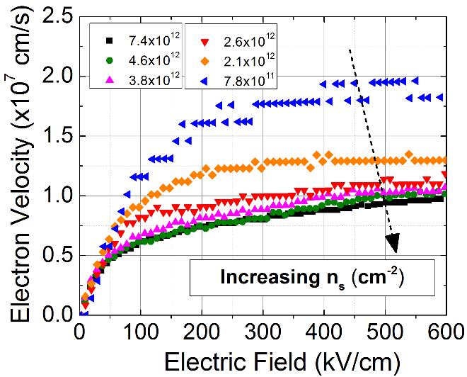
4 using scanning electron microscope to confirm an error of ~ 2% as shown in Figures 2(c) and 2(d). To obtain different sheet charge densities, low-damage ICP-RIE etching was used (RIE power of ~ 3 Watts). Ohmic contact resistance of 0.4 Ω.mm was extracted using transmission length method measurements. For each recess depth, on-wafer Hall measurements were used to determine the sheet charge density and Hall mobility. The extracted values for electron sheet density and the corresponding mobility across several dies with different recess depths are shown in Figure 3. To measure the velocity-field curves, pulsed IV measurements were done using 2-terminal GS RF probes 16 and a commercial Dynamic IV Analyzer system 17. A pulse duration of 500ns with a duty cycle of 0.01% was used. The conditions were chosen to ensure that self-heating effects did not have significant impact on the measured data. To eliminate leakage currents from the buffer layers and the instrument, an adjacent mesa-isolated device was measured and subtracted from each active device I-V characteristic. Figure 4 shows an example of a series of pulsed measurements carried out at different sheet charge densities. The velocity profiles start to saturate above ~ 200 kv/cm, though the shape of the curves is different from different carrier density. There is negligible increase in the velocity beyond 500 kv/cm in all cases. At lower sheet charge density, the saturated velocity is significantly higher than that at higher sheet charge density. An increase in the noise level is also noticed with decreasing ns since the noise from the equipment is more evident as the device current density reduces. Using the velocity value at the maximum field (600 kv/cm) as the saturated velocity, the saturation velocity is plotted as a function of the 2DEG charge density. For each charge density, multiple devices were measured to verify uniformity, and the spread in the velocity is indicated through error bars. The saturation velocity at low sheet charge density is 1.9x10 7 cm/s, which is similar to that estimated by previous work in GaN 8,9,18. However, as the sheet charge density is increased above cm -2, the electron saturation velocity decreases significantly (by approximately 50%). As discussed later in this work, this velocity decrease 4
5 plays a critical role in device characteristics, including the current density, transconductance profile and small-signal parameters. Such a strong dependence of saturation velocity on the sheet charge density measured here cannot be explained by conventional mechanisms, such as band non-parabolicity and inter-valley transfer. One plausible cause may be related to hot phonons, or, more specifically to their stimulated emission. Previous works 19,20 have shown that the presence of hot phonons increases momentum relaxation time while not affecting the energy relaxation time a clear recipe for the velocity saturation. The hot LO phonons are prevalent in wide gap nitride semiconductors (unlike Si and GaAs) due to their relatively long (few picoseconds) lifetimes 21 τ LO. These early models have shown qualitative agreement with a few experimental data points available at a time, but did not faithfully reproduce the clear clamping that can be observed in Figure 4. The reason for it was that references 19 and 20 used standard Fermi-Dirac distribution function for which, as shown in Figure 6(a), the electron population in f the state with larger momentum 2 is always less than population of the state with a smaller momentum f 1. Therefore, the probability of absorption of LO phonon with momentum = 2 1 q k k is always stronger than stimulated emission. If, however one uses a more suitable model, with the so-called drifted Fermi-Dirac distribution 22 in which Fermi function is shifted by the amount of average drift momentum kd = mcvd /, then for v small drift velocity d the situation would not change significantly from Figure 6(a), but as vd increases, f > f the situation when 2 1 shown Figure 6(b) arises. Now the higher energy state k2 has larger population than the lower one k1, and, with probability of stimulated LO emission exceeding that of LO absorption, phonons now experience gain glo (per unit of time) that is naturally proportional to the carrier density. 5
6 This situation is entirely analogous to the photon gain in laser medium, and, just as in a laser, threshold condition gloτ LO > 1 is reached when the phonon gain exceeds phonon decay. At this point the density of LO phonons starts growing exponentially and velocity saturates as all the additional power gets immediately transferred to LO generation, just as the upper level population in the laser gets clamped at threshold. Clearly, the higher is the carrier density, the earlier is the threshold reached and velocity saturates at a lower value, although the exact dependence of saturation velocity on sheet density is complicated as electron temperature also changes with increase in current density. Performing selfconsistent simulations with drifted Fermi-Dirac distribution we have fitted the results into expression n 0 shown in Eq. (1) where S, is cm v Sat ( n ) = (1) S n S ns,0 The theoretical curve is displayed in Figure 5 and shows good agreement with the measured results, suggesting that the model explains strong dependence of saturation velocity on carrier concentration, and captures the physics of 2DEG transport in GaN rather well. To further verify the presented measurement results and model, the experimental sheet densitydependent saturation velocity characteristics were used in two-dimensional (2-D) TCAD simulator Silvaco ATLAS to simulate DC and RF characteristics of a reported GaN HEMT for comparison 23. The simulated device was a standard sub-100 nm AlGaN/GaN HEMT structure on SiC substrate, with 20 nm of AlGaN barrier layer, 1nm of AlN interlayer and GaN buffer. The source-to-drain distance, LSD, and the gate length, LG, were 1.1 µm, and 60 nm, respectively, and the heights of gate, hgate, was set to be 560 nm. The gate resistance, Rg, was 0.15 Ω mm, and contact resistance, Rc, was 0.23 Ω mm, as 6
7 described in [23]. Figure 7 shows the comparison between the simulated and the experimental transfer characteristics, current gain profile, and the output characteristics. Excellent agreement between the simulated and the experimental results validates the measured density-dependent electron transport in 2DEGs of GaN HEMTs, and illustrates the accurate prediction of their DC and RF characteristics using the measurement. This shows that using a density dependent velocity model is critical for predictive models of AlGaN/GaN HEMTs. In conclusion, we have measured the sheet density dependence of electron velocity in 2DEG of AlGaN/GaN HEMTs. The measured saturated velocity was found to have strong dependence on carrier density, and it reduced significantly with increasing density. A new optical phonon emission-based electron velocity model for GaN is presented and shown to capture the measured dependence rather well. The presented model accommodates stimulated LO phonon emission which clamps the electron velocity with strong electron-phonon interaction and long LO phonon lifetime in GaN. This clamping of the saturation velocity is found to be strongly dependent to electron carrier density in GaN channel. Finally, the measured density dependence of saturation velocity was applied in TCAD-based device simulator to simulate DC and small signal characteristics of a reported GaN HEMT with sub-100nm gate-length. Excellent agreement between the simulated and experimental results validated the measurement presented in this report and established accurate modeling of GaN HEMTs using the measured field and density dependence of electron velocity. The presented direct measurement of density-dependent electron velocity characteristics, new physics-based model, and precise simulation of DC and RF characteristics of GaN HEMTs have important applications in designing and enabling future III-Nitride transistors for high gain and linearity performance. The presented work could be used for minimizing the use of resources for the optimization of the transistor structure from the experimental studies, and 7
8 can also be used to provide the close-fit benchmark for the upcoming high-frequency mm-wave applications. Acknowledgement: The authors gratefully acknowledge the support from DATE MURI (ONR N , Dr. Paul Maki), EXEDE MURI (ONR N , Dr. Daniel Green and Dr. Paul Maki) and Raytheon Integrated Defense Systems, and the valuable help from Ye Shao and Prof. Wu Lu (The Ohio State University). 8
9 References: 1 Y. F. Wu, M. Moore, A. Saxler, T. Wisleder, & P. Parikh, 40-W/mm double field-plated GaN HEMTs, 64th Device Research Conference (2006). 2 Y. Yue, Z. Hu, J. Guo, B. Sensale-Rodriguez, G. Li, R. Wang, F. Faria, T. Fang, B. Song, X. Gao, S. Guo, T. Kosel, G. Snider, P. Fay, D. Jena & H. Xing, IEEE Electron Device Lett. 33(7), (2012) 3 K. Shinohara, D. Regan, A. Corrion, D. Brown, Y. Tang, J. Wong, G. Candia, A. Schmitz, H. Fung, S. Kim and M. Micovic, IEEE IEDM, (2012) 4 Y. Tang; K. Shinohara, D. Regan, A. Corrion, D. Brown, J. Wong, A. Schmitz, H. Fung, S. Kim, M. Micovic, IEEE Electron Device Lett. 36(6), (2015) 5 S. Dasgupta, D. F. Brown, F. Wu, S. Keller, J. S. Speck, & U. K. Mishra, Appl. Phys. Lett. 96(14), (2010). 6 P. S. Park, S. Krishnamoorthy, S. Bajaj, D. N. Nath, & S. Rajan, IEEE Electron Device Lett. 36(3), (2015). 7 U. V. Bhapkar and M. S. Shur, J. Appl. Phys. 82(4), (1997) 8 M. Farahmand, C. Garetto, E. Bellotti, K. F. Brennan, M. Goano, E. Ghillino, G. Ghione, J. D. Albrecht and P. P. Ruden, IEEE Trans. on Electron Devices, 48(3), (2001) 9 B. Gelmont, K. Kim, and M. Shur, J. Appl. Phys. 74(3), (1993) 10 S. K. O'Leary, B. E. Foutz, M. S. Shur, U. V. Bhapkar, and L. F. Eastman, Solid State Communications, 105(10), (1998) 9
10 11 A. Reklaitis and L. Reggiani, J. Appl. Phys. 95(12), (2004) 12 T. Fang, R. Wang, H. Xing, S. Rajan, and D. Jena, IEEE Electron Device Lett. 33(5), (2012) 13 P. Waltereit, C. Poblenz, S. Rajan, F. Wu, U. K. Mishra & J. S. Speck, Japanese J. Appl. Phys. 43(12A), L1520 (2004) 14 I. Khan and J. Cooper, IEEE Trans. on Electron Devices, 47(2), (2000) 15 B. A. Danilchenko, N. A. Tripachko, A. E. Belyaev, S. A. Vitusevich, H. Hardtdegen & H. Lüth, Appl. Phys. Lett. 104(7), (2014) 16 Cascade Mictrotech Inc., Beaverton, OR, USA 17 DiVA D265, Accent Optical Technologies Inc., Bend, OR, USA; Nanometrics Inc., Milpitas, CA, USA 18 M. Wraback, H. Shen, J. C. Carrano, T. Li, J. C. Campbell, M. J. Schurman & I. T. Ferguson, Appl. Phys. Lett. 76, 1155 (2000) 19 B. K. Ridley, W. J. Schaff, and L. F. Eastman, J. Appl. Phys. 96(3), (2004) 20 J. Khurgin, Y. Ding & D. Jena, Appl. Phys. Lett. 91(25), (2007) 21 K. T. Tsen, J. G. Kiang, D. K. Ferry and H. Morkoc, Appl. Phys. Lett. 89(11), 2111 (2006) 22 Ultrafast phenomena in Semiconductors, K-T Tsen, Editor, Springer, NY (2001) 23 J. W. Chung, W. E. Hoke, E. M. Chumbes, and T. Palacios, IEEE Electron Device Lett. 31(3), (2010) 24 M. Grundmann, "BandEng." Poisson Schrödinger solver software (2004). 10
11 Figure captions: Figure 1: AlGaN/GaN HEMT used for the study; (a) Structure schematic; and (b) the associated energy-band diagram. Figure 2: The I-shaped test structure used for electron transport measurements using 2-terminal RF probe; (a) isometric view; (b) micrograph and schematic; (c) SEM images of 2 μm x 2 μm and (d) a 5 μm x 5 μm constriction structures. Figure 3: Measured Hall mobility as a function of sheet charge density (ns) for different recesses using low-power plasma etch. On-wafer Hall measurements were done on van der Pauw structures. Inset: measured values of sheet charge density and the associated values of Hall mobility and estimated AlGaN barrier thickness 24. Figure 4: Measured sheet charge density (ns) dependent electron velocity-field characteristics for AlGaN/GaN HEMT plotted for various ns values. Figure 5: (a) Sheet charge density (ns) dependent electron saturation velocity (vsat) extracted from measured velocity-field characteristics. The error bars include the vsat values extracted from multiple devices. The data is compared to the presented optical phonon-based model. Figure 6: (a) Fermi-Dirac distribution for low drift velocity vd showing that for two states k1 and k2 probability of phonon absorption always exceeds that of stimulated emission (b) Femi-Dirac distribution for large vd showing that LO phonons experience electron-density-dependent gain that will eventually cause the velocity saturation. Figure 7: Comparison between the simulated and the experimental device characteristics from [23]; (a) transfer characteristics; (b) current gain profile; and (c) output characteristics. 11
12 1. 2.
13 3. 4.
14 5. 6.
15 7.
M R S Internet Journal of Nitride Semiconductor Research
 Page 1 of 6 M R S Internet Journal of Nitride Semiconductor Research Volume 9, Article 7 The Ambient Temperature Effect on Current-Voltage Characteristics of Surface-Passivated GaN-Based Field-Effect Transistors
Normally-Off GaN Field Effect Power Transistors: Device Design and Process Technology Development
 Center for High Performance Power Electronics Normally-Off GaN Field Effect Power Transistors: Device Design and Process Technology Development Dr. Wu Lu (614-292-3462, lu.173@osu.edu) Dr. Siddharth Rajan
Unipolar Vertical Transport in GaN/AlGaN/GaN Heterostructures
 Unipolar Vertical Transport in GaN/AlGaN/GaN Heterostructures D. N. Nath, P.S. Park, Z. C. Yang & S. Rajan The Ohio State University, Department of Electrical and Computer Engineering Columbus, OH, 4321
NUMERICAL CALCULATION OF THE ELECTRON MOBILITY IN GaAs SEMICONDUCTOR UNDER WEAK ELECTRIC FIELD APPLICATION
 International Journal of Science, Environment and Technology, Vol. 1, No 2, 80-87, 2012 NUMERICAL CALCULATION OF THE ELECTRON MOBILITY IN GaAs SEMICONDUCTOR UNDER WEAK ELECTRIC FIELD APPLICATION H. Arabshahi,
Analytical Evaluation of Energy and Electron Concentrations in Quantum Wells of the High Electron Mobility Transistors.
 Analytical Evaluation of Energy Electron Concentrations in Quantum Wells of the High Electron Mobility Transistors Salih SAYGI Department of Physics, Faculty of Arts Sciences, Gaziosmanpasa University,
Traps in MOCVD n-gan Studied by Deep Level Transient Spectroscopy and Minority Carrier Transient Spectroscopy
 Traps in MOCVD n-gan Studied by Deep Level Transient Spectroscopy and Minority Carrier Transient Spectroscopy Yutaka Tokuda Department of Electrical and Electronics Engineering, Aichi Institute of Technology,
Reliability Concerns due to Self-Heating Effects in GaN HEMTs
 Reliability Concerns due to Self-Heating Effects in GaN HEMTs B. Padmanabhan, D. Vasileska and S. M. Goodnick School of Electrical, Computer and Energy Engineering Arizona State University, Tempe, Arizona
POLARIZATION INDUCED EFFECTS IN AlGaN/GaN HETEROSTRUCTURES
 Vol. 98 (2000) ACTA PHYSICA POLONICA A No. 3 Proceedings of the XXIX International School of Semiconducting Compounds, Jaszowiec 2000 POLARIZATION INDUCED EFFECTS IN AlGaN/GaN HETEROSTRUCTURES O. AMBACHER
Role of Electrochemical Reactions in the Degradation Mechanisms of AlGaN/GaN HEMTs
 Role of Electrochemical Reactions in the Degradation Mechanisms of AlGaN/GaN HEMTs Feng Gao 1,2, Bin Lu 2, Carl V. Thompson 1, Jesús del Alamo 2, Tomás Palacios 2 1. Department of Materials Science and
Simulation of GaN-based Light-Emitting Devices
 Simulation of GaN-based Light-Emitting Devices Joachim Piprek Solid-State Lighting and Display Center Materials Department, College of Engineering University of California, Santa Barbara, CA 93106 piprek@ieee.org
Investigation of Hot Electrons and Hot Phonons Generated within an AlN/GaN High Electron Mobility Transistor
 ISSN 154-66X, Laser Physics, 9, Vol. 19, No. 4, pp. 745 751. Pleiades Publishing, Ltd., 9. Original Text Astro, Ltd., 9. MODERN TRENDS IN LASER PHYSICS Investigation of Hot Electrons and Hot Phonons Generated
OVER THE LAST several years, AIGaN/GaN HFETs
 588 IEEE TRANSACTIONS ON ELECTRON DEVICES, VOL. 53, NO. 4, APRIL 2006 Device Scaling Physics and Channel Velocities in AIGaN/GaN HFETs: Velocities and Effective Gate Length Yuh-Renn Wu, Student Member,
Strain and Temperature Dependence of Defect Formation at AlGaN/GaN High Electron Mobility Transistors on a Nanometer Scale
 Strain and Temperature Dependence of Defect Formation at AlGaN/GaN High Electron Mobility Transistors on a Nanometer Scale Chung-Han Lin Department of Electrical & Computer Engineering, The Ohio State
Supporting Online Material for
 www.sciencemag.org/cgi/content/full/327/5966/662/dc Supporting Online Material for 00-GHz Transistors from Wafer-Scale Epitaxial Graphene Y.-M. Lin,* C. Dimitrakopoulos, K. A. Jenkins, D. B. Farmer, H.-Y.
Electric Field-Dependent Charge-Carrier Velocity in Semiconducting Carbon. Nanotubes. Yung-Fu Chen and M. S. Fuhrer
 Electric Field-Dependent Charge-Carrier Velocity in Semiconducting Carbon Nanotubes Yung-Fu Chen and M. S. Fuhrer Department of Physics and Center for Superconductivity Research, University of Maryland,
Field effect = Induction of an electronic charge due to an electric field Example: Planar capacitor
 JFETs AND MESFETs Introduction Field effect = Induction of an electronic charge due to an electric field Example: Planar capacitor Why would an FET made of a planar capacitor with two metal plates, as
Electrical Properties Characterization of AlGaN/GaN MODFET
 RESEARCH INVENTY: International Journal of Engineering and Science ISSN: 2278-4721, Vol. 1, Issue 7 (November 2012), PP 62-70 www.researchinventy.com Electrical Properties Characterization of AlGaN/GaN
Dynamic On-resistance and Tunneling Based De-trapping in GaN HEMT
 MITSUBISHI ELECTRIC RESEARCH LABORATORIES http://www.merl.com Dynamic On-resistance and Tunneling Based De-trapping in GaN HEMT Zhu, L.; Teo, K.H.; Gao, Q. TR2015-047 June 2015 Abstract GaN HEMT dynamic
Performance Analysis of. doped and undoped AlGaN/GaN HEMTs
 Performance Analysis of doped and undoped AlGaN/GaN HEMTs Smitha G S 1, Meghana V 2, Narayan T. Deshpande 3 1 M. Tech Student, ECE, BMS College of Engineering, Bengaluru, Karnataka, India 2B.E. Student,
Controlling Graphene Ultrafast Hot Carrier Response from Metal-like. to Semiconductor-like by Electrostatic Gating
 Controlling Graphene Ultrafast Hot Carrier Response from Metal-like to Semiconductor-like by Electrostatic Gating S.-F. Shi, 1,2* T.-T. Tang, 1 B. Zeng, 1 L. Ju, 1 Q. Zhou, 1 A. Zettl, 1,2,3 F. Wang 1,2,3
Effects of Current Spreading on the Performance of GaN-Based Light-Emitting Diodes
 IEEE TRANSACTIONS ON ELECTRON DEVICES, VOL. 48, NO. 6, JUNE 2001 1065 Effects of Current Spreading on the Performance of GaN-Based Light-Emitting Diodes Hyunsoo Kim, Seong-Ju Park, and Hyunsang Hwang Abstract
Final Report for Army Research Office (ARO) and Dr. John Zavada. Report title:
 and Dr. John Zavada. Report title:") Final Report for Army Research Office (ARO) and Dr. John Zavada Report title: GaN light-emitting triodes (LETs) for high-efficiency hole injection and for assessment of the physical origin of the efficiency
Final Report for Army Research Office (ARO) and Dr. John Zavada Report title: GaN light-emitting triodes (LETs) for high-efficiency hole injection and for assessment of the physical origin of the efficiency
Electro-Thermal Transport in Silicon and Carbon Nanotube Devices E. Pop, D. Mann, J. Rowlette, K. Goodson and H. Dai
 Electro-Thermal Transport in Silicon and Carbon Nanotube Devices E. Pop, D. Mann, J. Rowlette, K. Goodson and H. Dai E. Pop, 1,2 D. Mann, 1 J. Rowlette, 2 K. Goodson 2 and H. Dai 1 Dept. of 1 Chemistry
Temperature Dependence of the Transport Properties of InN
 Temperature Dependence of the Transport Properties of InN G. Aloise, S. Vitanov, and V. Palankovski ADVANCED MATERIAS AND DEVICE ANAYSIS GROUP INST. FOR MICROEECTRONICS TU Wien, A-1040 Vienna, Austria
Influence of surface processing and passivation on carrier concentrations and transport properties in AlGaNÕGaN heterostructures
 JOURNAL OF APPLIED PHYSICS VOLUME 90, NUMBER 3 1 AUGUST 2001 Influence of surface processing and passivation on carrier concentrations and transport properties in AlGaNÕGaN heterostructures X. Z. Dang
Ultrafast All-optical Switches Based on Intersubband Transitions in GaN/AlN Multiple Quantum Wells for Tb/s Operation
 Ultrafast All-optical Switches Based on Intersubband Transitions in GaN/AlN Multiple Quantum Wells for Tb/s Operation Jahan M. Dawlaty, Farhan Rana and William J. Schaff Department of Electrical and Computer
Electron leakage effects on GaN-based light-emitting diodes
 Opt Quant Electron (2010) 42:89 95 DOI 10.1007/s11082-011-9437-z Electron leakage effects on GaN-based light-emitting diodes Joachim Piprek Simon Li Received: 22 September 2010 / Accepted: 9 January 2011
Impact of oxide thickness on gate capacitance Modelling and comparative analysis of GaN-based MOSHEMTs
 PRAMANA c Indian Academy of Sciences Vol. 85, No. 6 journal of December 2015 physics pp. 1221 1232 Impact of oxide thickness on gate capacitance Modelling and comparative analysis of GaN-based MOSHEMTs
The effect of light illumination in photoionization of deep traps in GaN MESFETs buffer layer using an ensemble Monte Carlo simulation
 International Journal of Physical Sciences Vol. 6(2), pp. 273-279, 18 January, 2011 Available online at http://www.academicjournals.org/ijps ISSN 1992-1950 2011 Academic Journals Full Length Research Paper
Simulation of Enhancement Mode GaN HEMTs with Threshold > 5 V using P-type Buffer
 1 imulation of Enhancement Mode GaN HEMTs with Threshold > 5 using -type Buffer anyam Bajaj, atih Akyol, riram Krishnamoorthy, Ting-Hsiang Hung and iddharth Rajan, Member, IEEE Abstract A high threshold
AlGaN/GaN-based HEMT on SiC substrate for microwave characteristics using different passivation layers
 PRAMANA c Indian Academy of Sciences Vol. 79, No. 1 journal of July 2012 physics pp. 151 163 AlGaN/GaN-based HEMT on SiC substrate for microwave characteristics using different passivation layers T R LENKA
ac ballistic transport in a two-dimensional electron gas measured in GaAs/ AlGaAs heterostructures
 ac ballistic transport in a two-dimensional electron gas measured in GaAs/ AlGaAs heterostructures Sungmu Kang and Peter J. Burke Henry Samueli School of Engineering, Electrical Engineering and Computer
GaN HEMT Reliability
 GaN HEMT Reliability J. A. del Alamo and J. Joh Microsystems Technology Laboratories, MIT ESREF 2009 Arcachon, Oct. 5-9, 2009 Acknowledgements: ARL (DARPA-WBGS program), ONR (DRIFT-MURI program) Jose Jimenez,
Studying of the Dipole Characteristic of THz from Photoconductors
 PIERS ONLINE, VOL. 4, NO. 3, 8 386 Studying of the Dipole Characteristic of THz from Photoconductors Hong Liu, Weili Ji, and Wei Shi School of Automation and Information Engineering, Xi an University of
SUPPLEMENTARY INFORMATION
 doi:10.1038/nature12036 We provide in the following additional experimental data and details on our demonstration of an electrically pumped exciton-polariton laser by supplementing optical and electrical
Device and Monte Carlo Simulation of GaN material and devices. Presenter: Ziyang Xiao Advisor: Prof. Neil Goldsman University of Maryland
 Device and Monte Carlo Simulation of GaN material and devices Presenter: Ziyang Xiao Advisor: Prof. Neil Goldsman University of Maryland 2/23 OUTLINE - GaN Introduction and Background Device Simulation
Influence of excitation frequency on Raman modes of In 1-x Ga x N thin films
 Influence of excitation frequency on Raman modes of In 1-x Ga x N thin films A. Dixit 1,, J. S. Thakur 2, V. M. Naik 3, R. Naik 2 1 Center of Excellence in Energy & ICT, Indian Institute of Technology
Quantum Phenomena & Nanotechnology (4B5)
") Quantum Phenomena & Nanotechnology (4B5) The 2-dimensional electron gas (2DEG), Resonant Tunneling diodes, Hot electron transistors Lecture 11 In this lecture, we are going to look at 2-dimensional electron
Quantum Phenomena & Nanotechnology (4B5) The 2-dimensional electron gas (2DEG), Resonant Tunneling diodes, Hot electron transistors Lecture 11 In this lecture, we are going to look at 2-dimensional electron
Microelectronics Reliability
 Microelectronics Reliability () 87 879 Contents lists available at SciVerse ScienceDirect Microelectronics Reliability journal homepage: www.elsevier.com/locate/microrel Impact of high-power stress on
Intraband emission of GaN quantum dots at λ =1.5 μm via resonant Raman scattering
 Intraband emission of GaN quantum dots at λ =1.5 μm via resonant Raman scattering L. Nevou, F. H. Julien, M. Tchernycheva, J. Mangeney Institut d Electronique Fondamentale, UMR CNRS 8622, University Paris-Sud
3-1-2 GaSb Quantum Cascade Laser
 3-1-2 GaSb Quantum Cascade Laser A terahertz quantum cascade laser (THz-QCL) using a resonant longitudinal optical (LO) phonon depopulation scheme was successfully demonstrated from a GaSb/AlSb material
GaN based transistors
 GaN based transistors S FP FP dielectric G SiO 2 Al x Ga 1-x N barrier i-gan Buffer i-sic D Transistors "The Transistor was probably the most important invention of the 20th Century The American Institute
Modelling of capacitance and threshold voltage for ultrathin normally-off AlGaN/GaN MOSHEMT
 Pramana J. Phys. (07) 88: 3 DOI 0.007/s043-06-30-y c Indian Academy of Sciences Modelling of capacitance and threshold voltage for ultrathin normally-off AlGaN/GaN MOSHEMT R SWAIN, K JENA and T R LENKA
Application II: The Ballistic Field-E ect Transistor
 Chapter 1 Application II: The Ballistic Field-E ect Transistor 1.1 Introduction In this chapter, we apply the formalism we have developed for charge currents to understand the output characteristics of
Monte Carlo Based Calculation of Electron Transport Properties in Bulk InAs, AlAs and InAlAs
 Bulg. J. Phys. 37 (2010) 215 222 Monte Carlo Based Calculation of Electron Transport Properties in Bulk InAs, AlAs and InAlAs H. Arabshahi 1, S. Golafrooz 2 1 Department of Physics, Ferdowsi University
Performance Analysis of Ultra-Scaled InAs HEMTs
 Purdue University Purdue e-pubs Birck and NCN Publications Birck Nanotechnology Center 2009 Performance Analysis of Ultra-Scaled InAs HEMTs Neerav Kharche Birck Nanotechnology Center and Purdue University,
Dual-metal-gate Structure of AlGaN/GaN MIS HEMTs Analysis and Design
 Dual-metal-gate Structure of AlGaN/GaN MIS HEMTs Analysis and Design Mr. Gaurav Phulwari 1, Mr. Manish Kumar 2 Electronics & Communication Engineering 1, 2, Bhagwant University, Ajmer 1,2 M.Tech Scholar
Ballistic transport at GHz frequencies in ungated HEMT structures
 Solid-State Electronics 8 (2) 23 27 www.elsevier.com/locate/sse Ballistic transport at GHz frequencies in ungated HEMT structures Sungmu Kang a, Peter J. Burke a, *, L.N. Pfeiffer b, K.W. West b a Henry
Recent Progress in Understanding the DC and RF Reliability of GaN High Electron Mobility Transistors
 Recent Progress in Understanding the DC and RF Reliability of GaN High Electron Mobility Transistors J. A. del Alamo and J. Joh* Microsystems Technology Laboratories, MIT, Cambridge, MA *Presently with
Supporting Information. by Hexagonal Boron Nitride
 Supporting Information High Velocity Saturation in Graphene Encapsulated by Hexagonal Boron Nitride Megan A. Yamoah 1,2,, Wenmin Yang 1,3, Eric Pop 4,5,6, David Goldhaber-Gordon 1 * 1 Department of Physics,
THE properties of high electron saturation velocity and
 4218 IEEE TRANSACTIONS ON ELECTRON DEVICES, VOL. 63, NO. 11, NOVEMBER 2016 AlGaN/GaN HEMTs on Silicon With Hybrid Schottky Ohmic Drain for RF Applications Chuan-Wei Tsou, Hsueh-Chun Kang, Yi-Wei Lian,
Supplementary material for High responsivity mid-infrared graphene detectors with antenna-enhanced photo-carrier generation and collection
 Supplementary material for High responsivity mid-infrared graphene detectors with antenna-enhanced photo-carrier generation and collection Yu Yao 1, Raji Shankar 1, Patrick Rauter 1, Yi Song 2, Jing Kong
Title: Ultrafast photocurrent measurement of the escape time of electrons and holes from
 Title: Ultrafast photocurrent measurement of the escape time of electrons and holes from carbon nanotube PN junction photodiodes Authors: Nathaniel. M. Gabor 1,*, Zhaohui Zhong 2, Ken Bosnick 3, Paul L.
3190 IEEE TRANSACTIONS ON ELECTRON DEVICES, VOL. 60, NO. 10, OCTOBER 2013
 3190 IEEE TRANSACTIONS ON ELECTRON DEVICES, VOL. 60, NO. 10, OCTOBER 2013 Methodology for the Study of Dynamic ON-Resistance in High-Voltage GaN Field-Effect Transistors Donghyun Jin, Student Member, IEEE,
Segmented 1.55um Laser with 400% Differential Quantum Efficiency J. Getty, E. Skogen, L. Coldren, University of California, Santa Barbara, CA.
 Segmented 1.55um Laser with 400% Differential Quantum Efficiency J. Getty, E. Skogen, L. Coldren, University of California, Santa Barbara, CA. Abstract: By electrically segmenting, and series-connecting
A novel model of photo-carrier screening effect on the GaN-based p-i-n ultraviolet detector
 049 SCIENCE CHINA Physics, Mechanics & Astronomy May 2010 Vol.53 No.5: 793 801 doi: 10.1007/s11433-010-0177-z A novel model of photo-carrier screening effect on the GaN-based p-i-n ultraviolet detector
Low-dimensional electron transport properties in InAs/AlGaSb mesoscopic structures
 Superlattices and Microstructures, Vol 21, No 1, 1997 Low-dimensional electron transport properties in InAs/AlGaSb mesoscopic structures M Inoue, T Sugihara, T Maemoto, S Sasa, H Dobashi, S Izumiya Department
Spring Semester 2012 Final Exam
 Spring Semester 2012 Final Exam Note: Show your work, underline results, and always show units. Official exam time: 2.0 hours; an extension of at least 1.0 hour will be granted to anyone. Materials parameters
Low frequency noise in GaNÕAlGaN heterostructure field effect transistors in non-ohmic region
 JOURNAL OF APPLIED PHYSICS VOLUME 93, NUMBER 1 15 JUNE 003 Low frequency noise in GaNÕAlGaN heterostructure field effect transistors in non-ohmic region S. L. Rumyantsev, a) N. Pala, b) and M. S. Shur
Soft Carrier Multiplication by Hot Electrons in Graphene
 Soft Carrier Multiplication by Hot Electrons in Graphene Anuj Girdhar 1,3 and J.P. Leburton 1,2,3 1) Department of Physics 2) Department of Electrical and Computer Engineering, and 3) Beckman Institute
An Overview of the analysis of two dimensional back illuminated GaAs MESFET
 An Overview of the analysis of two dimensional back illuminated GaAs MESFET Prof. Lochan Jolly*, Ms. Sonia Thalavoor** *(A.P- Department of Electronics & Telecommunication, TCET, Mumbai Email: lochan.jolly@thakureducation.org)
Multi-cycle THz pulse generation in poled lithium niobate crystals
 Laser Focus World April 2005 issue (pp. 67-72). Multi-cycle THz pulse generation in poled lithium niobate crystals Yun-Shik Lee and Theodore B. Norris Yun-Shik Lee is an assistant professor of physics
Dislocation scattering effect on two-dimensional electron gas transport in an GaN/AlGaN modulation-doped heterostructure
 Dislocation scattering effect on two-dimensional electron gas transport in an GaN/AlGaN modulation-doped heterostructure Sibel Gökden Balikesir University, Department of Physics, Balikesir-Turkey *Corresponding
Correlation between Current Collapse Phenomena and Deep-Level Defects in AlGaN/GaN Hetero-Structures Probed by Deep-Level Optical Spectroscopy
 総合工学第 23 巻 (211) 頁 Correlation between Current Collapse Phenomena and Deep-Level Defects in AlGaN/GaN Hetero-Structures Probed by Deep-Level Optical Spectroscopy Yoshitaka Nakano Abstract: We have investigated
JARA FIT Ferienprakticum Nanoelektronik Experiment: Resonant tunneling in quantum structures
 JARA FIT Ferienprakticum Nanoelektronik 2013 Experiment: Resonant tunneling in quantum structures Dr. Mihail Ion Lepsa, Peter Grünberg Institut (PGI 9), Forschungszentrum Jülich GmbH 1. Introduction The
Energy position of the active near-interface traps in metal oxide semiconductor field-effect transistors on 4H SiC
 Energy position of the active near-interface traps in metal oxide semiconductor field-effect transistors on 4H SiC Author Haasmann, Daniel, Dimitrijev, Sima Published 2013 Journal Title Applied Physics
NiCl2 Solution concentration. Etching Duration. Aspect ratio. Experiment Atmosphere Temperature. Length(µm) Width (nm) Ar:H2=9:1, 150Pa
 Width (nm) Ar:H2=9:1, 150Pa") Experiment Atmosphere Temperature #1 # 2 # 3 # 4 # 5 # 6 # 7 # 8 # 9 # 10 Ar:H2=9:1, 150Pa Ar:H2=9:1, 150Pa Ar:H2=9:1, 150Pa Ar:H2=9:1, 150Pa Ar:H2=9:1, 150Pa Ar:H2=9:1, 150Pa Ar:H2=9:1, 150Pa Ar:H2=9:1,
Experiment Atmosphere Temperature #1 # 2 # 3 # 4 # 5 # 6 # 7 # 8 # 9 # 10 Ar:H2=9:1, 150Pa Ar:H2=9:1, 150Pa Ar:H2=9:1, 150Pa Ar:H2=9:1, 150Pa Ar:H2=9:1, 150Pa Ar:H2=9:1, 150Pa Ar:H2=9:1, 150Pa Ar:H2=9:1,
Non-equilibrium Green s functions: Rough interfaces in THz quantum cascade lasers
 Non-equilibrium Green s functions: Rough interfaces in THz quantum cascade lasers Tillmann Kubis, Gerhard Klimeck Department of Electrical and Computer Engineering Purdue University, West Lafayette, Indiana
Supplementary Figure S1. AFM images of GraNRs grown with standard growth process. Each of these pictures show GraNRs prepared independently,
 Supplementary Figure S1. AFM images of GraNRs grown with standard growth process. Each of these pictures show GraNRs prepared independently, suggesting that the results is reproducible. Supplementary Figure
GaN light-emitting triodes for high-efficiency hole injection and light emission
 GaN light-emitting triodes for high-efficiency hole injection and light emission Jong Kyu Kim a,*, J.-Q. Xi a, Hong Luo a, Jaehee Cho b, Cheolsoo Sone b, Yongjo Park b, Thomas Gessmann a, J. M. Zavada
Ultrafast carrier dynamics in InGaN MQW laser diode
 Invited Paper Ultrafast carrier dynamics in InGaN MQW laser diode Kian-Giap Gan* a, Chi-Kuang Sun b, John E. Bowers a, and Steven P. DenBaars a a Department of Electrical and Computer Engineering, University
SIMULATION OF A Si/SiGe MODULATION-DOPED FET USING QUANTUM HYDRODYNAMIC EQUATIONS*
 SIMULATION OF A Si/SiGe MODULATION-DOPED FET USING QUANTUM HYDRODYNAMIC EQUATIONS* J.-R. Zhou, T. Yamada, H. Miyata +, and D. K. Ferry Center for Solid State Electronics Research Arizona State University,
Modeling Electron Emission From Diamond-Amplified Cathodes
 Modeling Electron Emission From Diamond-Amplified Cathodes D. A. Dimitrov Tech-X Corporation, Boulder, CO I. Ben-Zvi, T. Rao, J. Smedley, E. Wang, X. Chang Brookhaven National Lab, NY This work is funded
Simulation of AlGaN/Si and InN/Si ELECTRIC DEVICES
 Simulation of AlGaN/Si and InN/Si ELECTRIC DEVICES Zehor Allam 1, Abdelkader Hamdoune 2, Chahrazed Boudaoud 3, Asmaa Amrani 4,Aicha Soufi 5,Zakia Nakoul 6 Unity of Research Materials and Renewable Energies,
Supporting information
 Supporting information Design, Modeling and Fabrication of CVD Grown MoS 2 Circuits with E-Mode FETs for Large-Area Electronics Lili Yu 1*, Dina El-Damak 1*, Ujwal Radhakrishna 1, Xi Ling 1, Ahmad Zubair
Simulation of Quantum Cascade Lasers
 Lighting up the Semiconductor World Simulation of Quantum Cascade Lasers 2005-2010 Crosslight Software Inc. Lighting up the Semiconductor World A A Contents Microscopic rate equation approach Challenge
Industrial Applications of Ultrafast Lasers: From Photomask Repair to Device Physics
 Industrial Applications of Ultrafast Lasers: From Photomask Repair to Device Physics Richard Haight IBM TJ Watson Research Center PO Box 218 Yorktown Hts., NY 10598 Collaborators Al Wagner Pete Longo Daeyoung
Operation and Modeling of. The MOS Transistor. Second Edition. Yannis Tsividis Columbia University. New York Oxford OXFORD UNIVERSITY PRESS
 Operation and Modeling of The MOS Transistor Second Edition Yannis Tsividis Columbia University New York Oxford OXFORD UNIVERSITY PRESS CONTENTS Chapter 1 l.l 1.2 1.3 1.4 1.5 1.6 1.7 Chapter 2 2.1 2.2
HIGH POWER density [1], [2] and very high performance
![HIGH POWER density [1], [2] and very high performance](/thumbs/80/82311340.jpg "HIGH POWER density [1], [2] and very high performance") 1456 IEEE TRANSACTIONS ON ELECTRON DEVICES, VOL. 58, NO. 5, MAY 2011 Analytical Model for Power Switching GaN-Based HEMT Design Michele Esposto, Alessandro Chini, and Siddharth Rajan Abstract The GaN high-electron
1456 IEEE TRANSACTIONS ON ELECTRON DEVICES, VOL. 58, NO. 5, MAY 2011 Analytical Model for Power Switching GaN-Based HEMT Design Michele Esposto, Alessandro Chini, and Siddharth Rajan Abstract The GaN high-electron
Investigating extremely low resistance ohmic contacts to silicon carbide using a novel test structure
 Investigating extremely low resistance ohmic contacts to silicon carbide using a novel test structure Author Pan, Yue, M. Collins, Aaron, Algahtani, Fahid, W. Leech, Patrick, K. Reeves, Geoffrey, Tanner,
Pseudomorphic HEMT quantum well AlGaAs/InGaAs/GaAs with AlAs:δ-Si donor layer
 IOP Conference Series: Materials Science and Engineering PAPER OPEN ACCESS Pseudomorphic HEMT quantum well AlGaAs/InGaAs/GaAs with AlAs:δ-Si donor layer Related content - Pseudomorphic HEMT with Sn nanowires
Intrinsic Electronic Transport Properties of High. Information
 Intrinsic Electronic Transport Properties of High Quality and MoS 2 : Supporting Information Britton W. H. Baugher, Hugh O. H. Churchill, Yafang Yang, and Pablo Jarillo-Herrero Department of Physics, Massachusetts
Effect of Piezoelectric Polarization on Phonon Relaxation Rates in Binary Wurtzite Nitrides
 Effect of Piezoelectric Polarization on Phonon Relaxation Rates in Binary Wurtzite Nitrides Bijay Kumar Sahoo Department of Physics, N. I.T, Raipur, India. Email: bksahoo.phy@nitrr.ac.in Abstract The piezoelectric
Self-heating simulation of GaN-based metal-oxide-semiconductor high-electron-mobility transistors including hot electron and quantum effects
 JOURNAL OF APPLIED PHYSICS 100, 074501 2006 Self-heating simulation of GaN-based metal-oxide-semiconductor high-electron-mobility transistors including hot electron and quantum effects W. D. Hu, X. S.
Anisotropic spin splitting in InGaAs wire structures
 Available online at www.sciencedirect.com Physics Physics Procedia Procedia 3 (010) 00 (009) 155 159 000 000 14 th International Conference on Narrow Gap Semiconductors and Systems Anisotropic spin splitting
Resonant terahertz absorption by plasmons in grating-gate GaN HEMT structures
 Resonant terahertz absorption by plasmons in grating-gate GaN HEMT structures A.V. Muravjov* a, D.B. Veksler a, X. Hu b, R. Gaska b, N. Pala c, H. Saxena d, R.E. Peale d, M.S. Shur a a ECSE Department,
Electric Field Measurements in Atmospheric Pressure Electric Discharges
 70 th Gaseous Electronics Conference Pittsburgh, PA, November 6-10, 2017 Electric Field Measurements in Atmospheric Pressure Electric Discharges M. Simeni Simeni, B.M. Goldberg, E. Baratte, C. Zhang, K.
Multicolor Graphene Nanoribbon/Semiconductor Nanowire. Heterojunction Light-Emitting Diodes
 Multicolor Graphene Nanoribbon/Semiconductor Nanowire Heterojunction Light-Emitting Diodes Yu Ye, a Lin Gan, b Lun Dai, *a Hu Meng, a Feng Wei, a Yu Dai, a Zujin Shi, b Bin Yu, a Xuefeng Guo, b and Guogang
Detectors of the Cryogenic Dark Matter Search: Charge Transport and Phonon Emission in Ge 100 Crystals at 40 mk
 J Low Temp Phys (2008) 151: 443 447 DOI 10.1007/s10909-007-9666-5 Detectors of the Cryogenic Dark Matter Search: Charge Transport and Phonon Emission in Ge 100 Crystals at 40 mk K.M. Sundqvist B. Sadoulet
Ultrafast Lateral Photo-Dember Effect in Graphene. Induced by Nonequilibrium Hot Carrier Dynamics
 1 Ultrafast Lateral Photo-Dember Effect in Graphene Induced by Nonequilibrium Hot Carrier Dynamics Chang-Hua Liu, You-Chia Chang, Seunghyun Lee, Yaozhong Zhang, Yafei Zhang, Theodore B. Norris,*,, and
A transient electron transport analysis of bulk wurtzite zinc oxide
 A transient electron transport analysis of bulk wurtzite zinc oxide Walid A. Hadi, Michael S. Shur, and Stephen K. O Leary Citation: J. Appl. Phys. 112, 3372 (212); doi: 1.163/1.474527 View online: http://dx.doi.org/1.163/1.474527
The physical process analysis of the capacitance voltage characteristics of AlGaN/AlN/GaN high electron mobility transistors
 Chin. Phys. B Vol. 9, No. 9 200 097302 The physical process analysis of the capacitance voltage characteristics of AlGaN/AlN/GaN high electron mobility transistors Wang Xin-Hua, Zhao Miao, Liu Xin-Yu,
Transient Harman Measurement of the Cross-plane ZT of InGaAs/InGaAlAs Superlattices with Embedded ErAs Nanoparticles
 Transient Harman Measurement of the Cross-plane ZT of InGaAs/InGaAlAs Superlattices with Embedded ErAs Nanoparticles Rajeev Singh, Zhixi Bian, Gehong Zeng, Joshua Zide, James Christofferson, Hsu-Feng Chou,
(a) (b) Supplementary Figure 1. (a) (b) (a) Supplementary Figure 2. (a) (b) (c) (d) (e)
 (b) Supplementary Figure 1. (a) (b) (a) Supplementary Figure 2. (a) (b) (c) (d) (e)") (a) (b) Supplementary Figure 1. (a) An AFM image of the device after the formation of the contact electrodes and the top gate dielectric Al 2 O 3. (b) A line scan performed along the white dashed line
(a) (b) Supplementary Figure 1. (a) An AFM image of the device after the formation of the contact electrodes and the top gate dielectric Al 2 O 3. (b) A line scan performed along the white dashed line
Recent Progress in Understanding the Electrical Reliability of GaN High-Electron Mobility Transistors
 Recent Progress in Understanding the Electrical Reliability of GaN High-Electron Mobility Transistors J. A. del Alamo Microsystems Technology Laboratories Massachusetts Institute of Technology 2015 MRS
GaN-based Devices: Physics and Simulation
 GaN-based Devices: Physics and Simulation Joachim Piprek NUSOD Institute Collaborators Prof. Shuji Nakamura, UCSB Prof. Steve DenBaars, UCSB Dr. Stacia Keller, UCSB Dr. Tom Katona, now at S-ET Inc. Dr.
drift vel. [10 cm/s] electric field [kv/cm] drift vel. [10 cm/s] electric field [kv/cm] T = 300 K GaN GaAs AlN
![drift vel. [10 cm/s] electric field [kv/cm] drift vel. [10 cm/s] electric field [kv/cm] T = 300 K GaN GaAs AlN](/thumbs/71/65838781.jpg "drift vel. [10 cm/s] electric field [kv/cm] drift vel. [10 cm/s] electric field [kv/cm] T = 300 K GaN GaAs AlN") Pyroelectronics: Novel device concepts based on nitride interfaces G. Zandler, J. A. Majewski, and P. Vogl Physik-Department and Walter Schottky Institut, Technische Universitat Munchen, Am Coulombwall,
Pyroelectronics: Novel device concepts based on nitride interfaces G. Zandler, J. A. Majewski, and P. Vogl Physik-Department and Walter Schottky Institut, Technische Universitat Munchen, Am Coulombwall,
Solid Surfaces, Interfaces and Thin Films
 Hans Lüth Solid Surfaces, Interfaces and Thin Films Fifth Edition With 427 Figures.2e Springer Contents 1 Surface and Interface Physics: Its Definition and Importance... 1 Panel I: Ultrahigh Vacuum (UHV)
M R S Internet Journal of Nitride Semiconductor Research
 M R S Internet Journal of Nitride Semiconductor Research Volume 2, Article 25 Properties of the Biexciton and the Electron-Hole-Plasma in Highly Excited GaN J.-Chr. Holst, L. Eckey, A. Hoffmann, I. Broser
MSE 310/ECE 340: Electrical Properties of Materials Fall 2014 Department of Materials Science and Engineering Boise State University
 MSE 310/ECE 340: Electrical Properties of Materials Fall 2014 Department of Materials Science and Engineering Boise State University Practice Final Exam 1 Read the questions carefully Label all figures