Summary lecture VI. with the reduced mass and the dielectric background constant
|
|
|
- Domenic Paul
- 5 years ago
- Views:
Transcription
 characterizes quantum systems in a mixed state and builds")

1 Summary lecture VI Excitonic binding energy reads with the reduced mass and the dielectric background constant Δ Statistical operator (density matrix) characterizes quantum systems in a mixed state and builds the expectation value of observables To tackle the many-particle-induced hierarchy problem, we perform the correlation expansion followed by a systematic truncation resulting in semiconductor Bloch equations on Hartree-Fock level
2 Graphene Bloch equations 2. Semiconductor Bloch equations Coupled system of differential equations on Hartree-Fock level Interaction-free contribution (kinetic energy) leads to an oscillation of the microscopic polarization p k (t)
3 Graphene Bloch equations 2. Semiconductor Bloch equations Coupled system of differential equations on Hartree-Fock level Electron-light coupling is determined by the Rabi frequency giving rise to a non-equilibrium distribution of electrons after optical excitation
4 Graphene Bloch equations 2. Semiconductor Bloch equations Coupled system of differential equations on Hartree-Fock level Electron-electron interaction leads to renormalization of energy and Rabi frequency (excitons!) as well as to dephasing of the polarization γ k


5 Microscopic polarization 2. Semiconductor Bloch equations Optical excitation with a laser pulse with an excitation energy of 1.5 ev Frequency of the oscillation of the microscopic polarization changes due to the Coulomb interaction
6 Non-equilibrium carrier distribution 2. Semiconductor Bloch equations Optical excitation with a laser pulse with an excitation energy of 1.5 ev We generate a non-equilibrium carrier distribution around the excitation energy (corresponding momentum k 0 = 1.25 nm -1 ) Fermi distribution Non-equilibrium carrier distribution


7 Anisotropic carrier distribution 2. Semiconductor Bloch equations 90 o 0 o Generation of an anisotropic non-equilibrium carrier distribution Maximal occupation perpendicular to polarization of excitation pulse (90 o ) due to the anisotropy of the optical matrix element Carrier dynamics needs to be modelled by extending Bloch equations beyond the Hartree-Fock approximation (Boltzmann equation)
8 Learning outcomes lecture VII Sketch the derivation of the Boltzmann scattering equation Explain the Markov approximation Describe the carrier dynamics in graphene Recognize the potential of carrier multiplication
9 Chapter IV IV. Density matrix theory 1. Statistical operator 2. Semiconductor Bloch equations 3. Boltzmann scattering equation
10 Second-order Born approximation Extend the correlation expansion to the second-order Born approximation explicitly taking into account the dynamics of 2-particle quantities Recap of the many-particle hierarchy problem (system of equations is not closed) Systematic truncation at the second order, i.e. we calculate the dynamics of 2-particle quantities, but neglect the contribution of three-particle quantities or higher
11 Second-order Born approximation The full Coulomb contribution to the dynamics of the carrier occupation Apply again the Heisenberg equation to botain the temporal evolution of the two-particle quantities

12 Second-order Born approximation Correlation expansion of the three-particle quantities with single-particle quantities and correlation quantities Now neglect the three-particle correlation quantity expression in the equation for and plug the
13 Markov approximation For 2-dimensional materials, such as graphene, with the compound indices A = (k x, k y, λ A ), the evaluation of full equations is a numerical challenging Markov approximation is applied neglecting quantum-mechanical memory effects stemming from energy-time uncertainty principle Inhomogeneous differential equation with the inhomogeneous part containing integrals over all scattering contributions and the convergence factor γ that will be sent to 0 at the end
14 Markov approximation The formal solution of the inhomogeneous differential equation reads Neglecting memory effects we find Finally, taking the limit


15 Boltzmann scattering equation Applying the second-order Born-Markov approximation, we obtain the Boltzmann scattering equation The equation describes time- and momentumresolved electron-electron scattering dynamics Pauli-blocking energy conservation


16 Boltzmann scattering equation Applying the second-order Born-Markov approximation, we obtain the Boltzmann scattering equation The equation describes time- and momentumresolved electron-electron scattering dynamics phonon absorption phonon emission

17 Carrier dynamics in graphene Non-equilibrium distribution


18 Carrier thermalization Significant relaxation takes place already during the excitation pulse
19 Carrier thermalization Significant relaxation takes place already during the excitation pulse Coulomb-induced carrier-carrier scattering is the dominant channel

20 Carrier thermalization Significant relaxation takes place already during the excitation pulse Coulomb-induced carrier-carrier scattering is the dominant channel Thermalized Fermi distribution reached within the first 50 fs
 are more efficient than acoustic")
21 Carrier cooling Carrier cooling takes place on a picosecond time scale Optical phonons (in particular ΓLO, ΓTO and K phonons) are more efficient than acoustic phonons
22 Relaxation dynamics in graphene


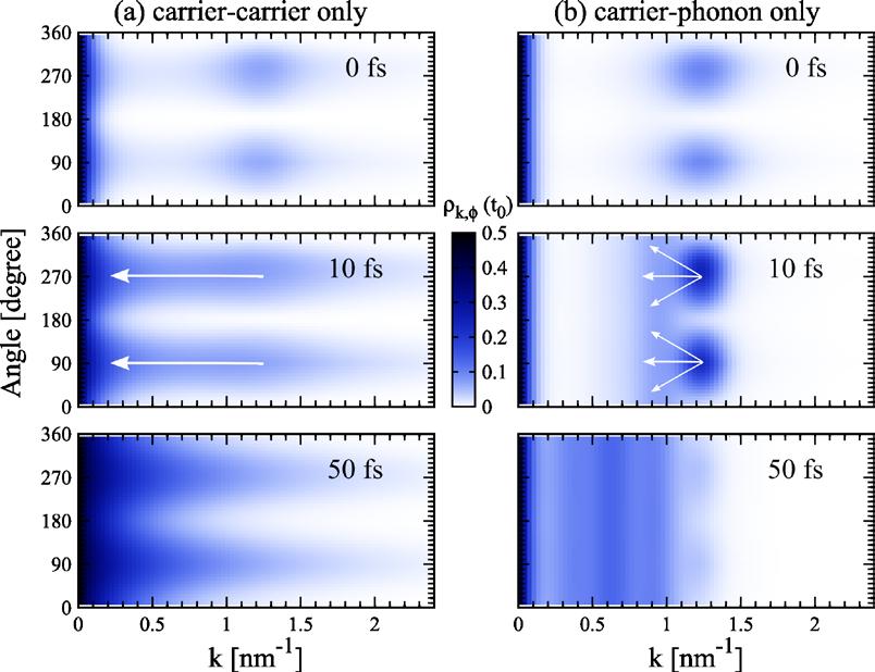
23 Anisotropic carrier dynamics Angle Anisotropy of the carrier-light coupling element


24 Anisotropic carrier dynamics Anisotropy of the carrier-light coupling element Scatering across the Dirac cone reduces anisotropy


25 Anisotropic carrier dynamics Anisotropy of the carrier-light coupling element Scatering across the Dirac cone reduces anisotropy Carrier distribution becomes entirely isotropic within the first 50 fs

26 Microscopic mechanism
27 Auger scattering Auger scattering changes the number of charge carriers in the system Auger recombination (AR) Impact ionization (II)

 Impact")
28 Impact excitation Auger scattering changes the number of charge carriers in the system Auger recombination (AR) Impact ionization (II) II
29 Impact excitation Auger scattering changes the number of charge carriers in the system Auger recombination (AR) Impact ionization (II) II
 Auger scattering is inefficient due to energy and momentum conservation carrier multiplication")
30 Carrier multiplication Auger scattering changes the number of charge carriers in the system Auger recombination (AR) Impact ionization (II) II gained electron in conduction band gained hole in valence band In conventional semiconductors (band gap) Auger scattering is inefficient due to energy and momentum conservation carrier multiplication (CM)
31 Carrier multiplication Carrier density increases during the excitation pulse

32 Carrier multiplication Carrier density increases during the excitation pulse Auger scattering leads to carrier multiplication (CM)

 Carrier-phonon scattering reduces CM on a")
33 Carrier multiplication Carrier density increases during the excitation pulse Auger scattering leads to carrier multiplication (CM) Carrier-phonon scattering reduces CM on a ps time scale
34 Learning outcomes lecture VII Sketch the derivation of the Boltzmann scattering equation Explain the Markov approximation Describe the carrier dynamics in graphene Recognize the potential of carrier multiplication
Summary lecture VII. Boltzmann scattering equation reads in second-order Born-Markov approximation
 Summary lecture VII Boltzmann scattering equation reads in second-order Born-Markov approximation and describes time- and momentum-resolved electron scattering dynamics in non-equilibrium Markov approximation
Summary lecture IX. The electron-light Hamilton operator reads in second quantization
 Summary lecture IX The electron-light Hamilton operator reads in second quantization Absorption coefficient α(ω) is given by the optical susceptibility Χ(ω) that is determined by microscopic polarization
Summary lecture II. Graphene exhibits a remarkable linear and gapless band structure
 Summary lecture II Bloch theorem: eigen functions of an electron in a perfectly periodic potential have the shape of plane waves modulated with a Bloch factor that possess the periodicity of the potential
Microscopic Modelling of the Optical Properties of Quantum-Well Semiconductor Lasers
 Microscopic Modelling of the Optical Properties of Quantum-Well Semiconductor Lasers Stephan W. Koch Department of Physics Philipps University, Marburg/Germany OVERVIEW - Outline of Theory - Gain/Absorption
Condensed matter physics FKA091
 Condensed matter physics FKA091 Ermin Malic Department of Physics Chalmers University of Technology Henrik Johannesson Department of Physics University of Gothenburg Teaching assistants: Roland Jago &
QUANTUM WELLS, WIRES AND DOTS
 QUANTUM WELLS, WIRES AND DOTS Theoretical and Computational Physics of Semiconductor Nanostructures Second Edition Paul Harrison The University of Leeds, UK /Cf}\WILEY~ ^INTERSCIENCE JOHN WILEY & SONS,
ESE 372 / Spring 2013 / Lecture 5 Metal Oxide Semiconductor Field Effect Transistor
 Metal Oxide Semiconductor Field Effect Transistor V G V G 1 Metal Oxide Semiconductor Field Effect Transistor We will need to understand how this current flows through Si What is electric current? 2 Back
Electronic and Optoelectronic Properties of Semiconductor Structures
 Electronic and Optoelectronic Properties of Semiconductor Structures Jasprit Singh University of Michigan, Ann Arbor CAMBRIDGE UNIVERSITY PRESS CONTENTS PREFACE INTRODUCTION xiii xiv 1.1 SURVEY OF ADVANCES
Ultrafast Spectroscopy of Semiconductors and Semiconductor Nanostructures
 Springer Series in Solid-State Sciences 115 Ultrafast Spectroscopy of Semiconductors and Semiconductor Nanostructures Bearbeitet von Jagdeep Shah erweitert 1999. Buch. xvi, 522 S. Hardcover ISBN 978 3
Basic Principles of Light Emission in Semiconductors
 Basic Principles of Light Emission in Semiconductors Class: Integrated Photonic Devices Time: Fri. 8:00am ~ 11:00am. Classroom: 資電 06 Lecturer: Prof. 李明昌 (Ming-Chang Lee) Model for Light Generation and
Optical Properties of Lattice Vibrations
 Optical Properties of Lattice Vibrations For a collection of classical charged Simple Harmonic Oscillators, the dielectric function is given by: Where N i is the number of oscillators with frequency ω
Metals: the Drude and Sommerfeld models p. 1 Introduction p. 1 What do we know about metals? p. 1 The Drude model p. 2 Assumptions p.
 Metals: the Drude and Sommerfeld models p. 1 Introduction p. 1 What do we know about metals? p. 1 The Drude model p. 2 Assumptions p. 2 The relaxation-time approximation p. 3 The failure of the Drude model
Lecture 1 - Electrons, Photons and Phonons. September 4, 2002
 6.720J/3.43J - Integrated Microelectronic Devices - Fall 2002 Lecture 1-1 Lecture 1 - Electrons, Photons and Phonons Contents: September 4, 2002 1. Electronic structure of semiconductors 2. Electron statistics
Semiconductor Physics and Devices Chapter 3.
 Introduction to the Quantum Theory of Solids We applied quantum mechanics and Schrödinger s equation to determine the behavior of electrons in a potential. Important findings Semiconductor Physics and
Deterministic Coherent Writing and Control of the Dark Exciton Spin using Short Single Optical Pulses
 Deterministic Coherent Writing and Control of the Dark Exciton Spin using Short Single Optical Pulses Ido Schwartz, Dan Cogan, Emma Schmidgall, Liron Gantz, Yaroslav Don and David Gershoni The Physics
Soft Carrier Multiplication by Hot Electrons in Graphene
 Soft Carrier Multiplication by Hot Electrons in Graphene Anuj Girdhar 1,3 and J.P. Leburton 1,2,3 1) Department of Physics 2) Department of Electrical and Computer Engineering, and 3) Beckman Institute
Lecture 3: Optical Properties of Insulators, Semiconductors, and Metals. 5 nm
 Metals Lecture 3: Optical Properties of Insulators, Semiconductors, and Metals 5 nm Course Info Next Week (Sept. 5 and 7) no classes First H/W is due Sept. 1 The Previous Lecture Origin frequency dependence
Energy Band Calculations for Dynamic Gain Models in Semiconductor Quantum Well Lasers
 Energy Band Calculations for Dynamic Gain Models in School of Electrical and Electronic Engineering University of Nottingham; Nottingham NG7 2RD; UK Email: eexpjb1@nottingham.ac.uk Presentation Outline
PHYSICS OF SEMICONDUCTORS AND THEIR HETEROSTRUCTURES
 PHYSICS OF SEMICONDUCTORS AND THEIR HETEROSTRUCTURES Jasprit Singh University of Michigan McGraw-Hill, Inc. New York St. Louis San Francisco Auckland Bogota Caracas Lisbon London Madrid Mexico Milan Montreal
Spins and spin-orbit coupling in semiconductors, metals, and nanostructures
 B. Halperin Spin lecture 1 Spins and spin-orbit coupling in semiconductors, metals, and nanostructures Behavior of non-equilibrium spin populations. Spin relaxation and spin transport. How does one produce
arxiv: v2 [cond-mat.mes-hall] 6 Apr 2011
![arxiv: v2 [cond-mat.mes-hall] 6 Apr 2011](/thumbs/72/66469363.jpg "arxiv: v2 [cond-mat.mes-hall] 6 Apr 2011") Electron spin relaxation as evidence of excitons in a two dimensional electron-hole plasma arxiv:1103.2474v2 [cond-mat.mes-hall] 6 Apr 2011 S. Oertel, 1 S. Kunz, 1 D. Schuh, 2 W. Wegscheider, 3 J. Hübner,
Electron spin relaxation as evidence of excitons in a two dimensional electron-hole plasma arxiv:1103.2474v2 [cond-mat.mes-hall] 6 Apr 2011 S. Oertel, 1 S. Kunz, 1 D. Schuh, 2 W. Wegscheider, 3 J. Hübner,
PRESENTED BY: PROF. S. Y. MENSAH F.A.A.S; F.G.A.A.S UNIVERSITY OF CAPE COAST, GHANA.
 SOLAR CELL AND ITS APPLICATION PRESENTED BY: PROF. S. Y. MENSAH F.A.A.S; F.G.A.A.S UNIVERSITY OF CAPE COAST, GHANA. OUTLINE OF THE PRESENTATION Objective of the work. A brief introduction to Solar Cell
Supplementary Figure S1 Definition of the wave vector components: Parallel and perpendicular wave vector of the exciton and of the emitted photons.
 Supplementary Figure S1 Definition of the wave vector components: Parallel and perpendicular wave vector of the exciton and of the emitted photons. Supplementary Figure S2 The calculated temperature dependence
Quantum Theory of the Optical and Electronic Properties of Semiconductors Downloaded from
 This page intentionally left blank Published by World Scientific Publishing Co. Pte. Ltd. 5 Toh Tuck Link, Singapore 596224 USA office: 27 Warren Street, Suite 401-402, Hackensack, NJ 07601 UK office:
Nanoscale Energy Transport and Conversion A Parallel Treatment of Electrons, Molecules, Phonons, and Photons
 Nanoscale Energy Transport and Conversion A Parallel Treatment of Electrons, Molecules, Phonons, and Photons Gang Chen Massachusetts Institute of Technology OXFORD UNIVERSITY PRESS 2005 Contents Foreword,
Sheng S. Li. Semiconductor Physical Electronics. Second Edition. With 230 Figures. 4) Springer
 Springer") Sheng S. Li Semiconductor Physical Electronics Second Edition With 230 Figures 4) Springer Contents Preface 1. Classification of Solids and Crystal Structure 1 1.1 Introduction 1 1.2 The Bravais Lattice
Sheng S. Li Semiconductor Physical Electronics Second Edition With 230 Figures 4) Springer Contents Preface 1. Classification of Solids and Crystal Structure 1 1.1 Introduction 1 1.2 The Bravais Lattice
Multiple Exciton Generation in Quantum Dots. James Rogers Materials 265 Professor Ram Seshadri
 Multiple Exciton Generation in Quantum Dots James Rogers Materials 265 Professor Ram Seshadri Exciton Generation Single Exciton Generation in Bulk Semiconductors Multiple Exciton Generation in Bulk Semiconductors
Luminescence Process
 Luminescence Process The absorption and the emission are related to each other and they are described by two terms which are complex conjugate of each other in the interaction Hamiltonian (H er ). In an
Elastic and Inelastic Scattering in Electron Diffraction and Imaging
 Elastic and Inelastic Scattering in Electron Diffraction and Imaging Contents Introduction Symbols and definitions Part A Diffraction and imaging of elastically scattered electrons Chapter 1. Basic kinematical
Exciton spectroscopy
 Lehrstuhl Werkstoffe der Elektrotechnik Exciton spectroscopy in wide bandgap semiconductors Lehrstuhl Werkstoffe der Elektrotechnik (WW6), Universität Erlangen-Nürnberg, Martensstr. 7, 91058 Erlangen Vortrag
Theory for strongly coupled quantum dot cavity quantum electrodynamics
 Folie: 1 Theory for strongly coupled quantum dot cavity quantum electrodynamics Alexander Carmele OUTLINE Folie: 2 I: Introduction and Motivation 1.) Atom quantum optics and advantages of semiconductor
Supplementary Information
 Ultrafast Dynamics of Defect-Assisted Electron-Hole Recombination in Monolayer MoS Haining Wang, Changjian Zhang, and Farhan Rana School of Electrical and Computer Engineering, Cornell University, Ithaca,
Semiconductor Physical Electronics
 Semiconductor Physical Electronics Sheng S. Li Department of Electrical Engineering University of Florida Gainesville, Florida Plenum Press New York and London Contents CHAPTER 1. Classification of Solids
Direct and Indirect Semiconductor
 Direct and Indirect Semiconductor Allowed values of energy can be plotted vs. the propagation constant, k. Since the periodicity of most lattices is different in various direction, the E-k diagram must
Intensity / a.u. 2 theta / deg. MAPbI 3. 1:1 MaPbI 3-x. Cl x 3:1. Supplementary figures
 Intensity / a.u. Supplementary figures 110 MAPbI 3 1:1 MaPbI 3-x Cl x 3:1 220 330 0 10 15 20 25 30 35 40 45 2 theta / deg Supplementary Fig. 1 X-ray Diffraction (XRD) patterns of MAPbI3 and MAPbI 3-x Cl
Minimal Update of Solid State Physics
 Minimal Update of Solid State Physics It is expected that participants are acquainted with basics of solid state physics. Therefore here we will refresh only those aspects, which are absolutely necessary
Contents Preface Physical Constants, Units, Mathematical Signs and Symbols Introduction Kinetic Theory and the Boltzmann Equation
 V Contents Preface XI Physical Constants, Units, Mathematical Signs and Symbols 1 Introduction 1 1.1 Carbon Nanotubes 1 1.2 Theoretical Background 4 1.2.1 Metals and Conduction Electrons 4 1.2.2 Quantum
LECTURES ON QUANTUM MECHANICS
 LECTURES ON QUANTUM MECHANICS GORDON BAYM Unitsersity of Illinois A II I' Advanced Bock Progrant A Member of the Perseus Books Group CONTENTS Preface v Chapter 1 Photon Polarization 1 Transformation of
Electron-phonon scattering (Finish Lundstrom Chapter 2)
") Electron-phonon scattering (Finish Lundstrom Chapter ) Deformation potentials The mechanism of electron-phonon coupling is treated as a perturbation of the band energies due to the lattice vibration. Equilibrium
Electron-phonon scattering (Finish Lundstrom Chapter ) Deformation potentials The mechanism of electron-phonon coupling is treated as a perturbation of the band energies due to the lattice vibration. Equilibrium
Optical Properties of Semiconductors. Prof.P. Ravindran, Department of Physics, Central University of Tamil Nadu, India
 Optical Properties of Semiconductors 1 Prof.P. Ravindran, Department of Physics, Central University of Tamil Nadu, India http://folk.uio.no/ravi/semi2013 Light Matter Interaction Response to external electric
CONTENTS. vii. CHAPTER 2 Operators 15
 CHAPTER 1 Why Quantum Mechanics? 1 1.1 Newtonian Mechanics and Classical Electromagnetism 1 (a) Newtonian Mechanics 1 (b) Electromagnetism 2 1.2 Black Body Radiation 3 1.3 The Heat Capacity of Solids and
Basic Semiconductor Physics
 Chihiro Hamaguchi Basic Semiconductor Physics With 177 Figures and 25 Tables Springer 1. Energy Band Structures of Semiconductors 1 1.1 Free-Electron Model 1 1.2 Bloch Theorem 3 1.3 Nearly Free Electron
Lecture 6. Fermion Pairing. WS2010/11: Introduction to Nuclear and Particle Physics
 Lecture 6 Fermion Pairing WS2010/11: Introduction to Nuclear and Particle Physics Experimental indications for Cooper-Pairing Solid state physics: Pairing of electrons near the Fermi surface with antiparallel
Chapter 12: Semiconductors
 Chapter 12: Semiconductors Bardeen & Shottky January 30, 2017 Contents 1 Band Structure 4 2 Charge Carrier Density in Intrinsic Semiconductors. 6 3 Doping of Semiconductors 12 4 Carrier Densities in Doped
Topic 11-3: Fermi Levels of Intrinsic Semiconductors with Effective Mass in Temperature
 Topic 11-3: Fermi Levels of Intrinsic Semiconductors with Effective Mass in Temperature Summary: In this video we aim to get an expression for carrier concentration in an intrinsic semiconductor. To do
Impact Ionization Can Explain Carrier Multiplication in PbSe Quantum Dots
 Impact Ionization Can Explain Carrier Multiplication in PbSe Quantum Dots A. Franceschetti,* J. M. An, and A. Zunger National Renewable Energy Laboratory, Golden, Colorado 8040 Received May 3, 2006; Revised
Solid State Physics. GIUSEPPE GROSSO Professor of Solid State Physics, Department of Physics, University of Pavia, and INFM
 Solid State Physics GIUSEPPE GROSSO Professor of Solid State Physics, Department of Physics, University of Pisa, and INFM GIUSEPPE PASTORI PARRAVICINI Professor of Solid State Physics, Department of Physics,
Non-equilibrium Green s functions: Rough interfaces in THz quantum cascade lasers
 Non-equilibrium Green s functions: Rough interfaces in THz quantum cascade lasers Tillmann Kubis, Gerhard Klimeck Department of Electrical and Computer Engineering Purdue University, West Lafayette, Indiana
Excitonic luminescence upconversion in a two-dimensional semiconductor
 Excitonic luminescence upconversion in a two-dimensional semiconductor Authors: Aaron M. Jones 1, Hongyi Yu 2, John R. Schaibley 1, Jiaqiang Yan 3,4, David G. Mandrus 3-5, Takashi Taniguchi 6, Kenji Watanabe
Quantum Condensed Matter Physics Lecture 9
 Quantum Condensed Matter Physics Lecture 9 David Ritchie QCMP Lent/Easter 2018 http://www.sp.phy.cam.ac.uk/drp2/home 9.1 Quantum Condensed Matter Physics 1. Classical and Semi-classical models for electrons
Optical Properties of Solid from DFT
 Optical Properties of Solid from DFT 1 Prof.P. Ravindran, Department of Physics, Central University of Tamil Nadu, India & Center for Materials Science and Nanotechnology, University of Oslo, Norway http://folk.uio.no/ravi/cmt15
Optics and Quantum Optics with Semiconductor Nanostructures. Overview
 Optics and Quantum Optics with Semiconductor Nanostructures Stephan W. Koch Department of Physics, Philipps University, Marburg/Germany and Optical Sciences Center, University of Arizona, Tucson/AZ Overview
ELECTRONS AND PHONONS IN SEMICONDUCTOR MULTILAYERS
 ELECTRONS AND PHONONS IN SEMICONDUCTOR MULTILAYERS В. К. RIDLEY University of Essex CAMBRIDGE UNIVERSITY PRESS Contents Introduction 1 Simple Models of the Electron-Phonon Interaction 1.1 General remarks
Lecture 15: Optoelectronic devices: Introduction
 Lecture 15: Optoelectronic devices: Introduction Contents 1 Optical absorption 1 1.1 Absorption coefficient....................... 2 2 Optical recombination 5 3 Recombination and carrier lifetime 6 3.1
nano.tul.cz Inovace a rozvoj studia nanomateriálů na TUL
 Inovace a rozvoj studia nanomateriálů na TUL nano.tul.cz Tyto materiály byly vytvořeny v rámci projektu ESF OP VK: Inovace a rozvoj studia nanomateriálů na Technické univerzitě v Liberci Units for the
Physics of atoms and molecules
 Physics of atoms and molecules 2nd edition B.H. Bransden and C.J. Joachain Prentice Hall An imprint of Pearson Education Harlow, England London New York Boston San Francisco Toronto Sydney Singapore Hong
Lecture 18: Semiconductors - continued (Kittel Ch. 8)
") Lecture 18: Semiconductors - continued (Kittel Ch. 8) + a - Donors and acceptors J U,e e J q,e Transport of charge and energy h E J q,e J U,h Physics 460 F 2006 Lect 18 1 Outline More on concentrations
Lecture 18: Semiconductors - continued (Kittel Ch. 8) + a - Donors and acceptors J U,e e J q,e Transport of charge and energy h E J q,e J U,h Physics 460 F 2006 Lect 18 1 Outline More on concentrations
Carrier Recombination
 Notes for ECE-606: Spring 013 Carrier Recombination Professor Mark Lundstrom Electrical and Computer Engineering Purdue University, West Lafayette, IN USA lundstro@purdue.edu /19/13 1 carrier recombination-generation
The Physics of Semiconductors
 The Physics of Semiconductors with applications to optoelectronic devices KEVIN F. BRENNAN CAMBRIDGE UNIVERSITY PRESS Contents Preface page xi Chapter1 Basic Concepts in Quantum Mechanics 1.1 Introduction
doi: /PhysRevLett
 doi: 10.1103/PhysRevLett.77.494 Luminescence Hole Burning and Quantum Size Effect of Charged Excitons in CuCl Quantum Dots Tadashi Kawazoe and Yasuaki Masumoto Institute of Physics and Center for TARA
More Efficient Solar Cells via Multi Exciton Generation
 More Efficient Solar Cells via Multi Exciton Generation By: MIT Student Instructor: Gang Chen May 14, 2010 1 Introduction Sunlight is the most abundant source of energy available on Earth and if properly
Dynamics of electrons in surface states with large spin-orbit splitting. L. Perfetti, Laboratoire des Solides Irradiés
 Dynamics of electrons in surface states with large spin-orbit splitting L. Perfetti, Laboratoire des Solides Irradiés Outline Topology of surface states on the Bi(111) surface Spectroscopy of electronic
Physics of Low-Dimensional Semiconductor Structures
 Physics of Low-Dimensional Semiconductor Structures Edited by Paul Butcher University of Warwick Coventry, England Norman H. March University of Oxford Oxford, England and Mario P. Tosi Scuola Normale
Time Resolved Pump-Probe Reflectivity in GaAs and GaN
 Time Resolved Pump-Probe Reflectivity in GaAs and GaN S. S. Prabhu * and A. S. Vengurlekar Department of Condensed Matter Physics and Material Science, Tata Institute of Fundamental Research, Homi Bhabha
Optical Characterization of Solids
 D. Dragoman M. Dragoman Optical Characterization of Solids With 184 Figures Springer 1. Elementary Excitations in Solids 1 1.1 Energy Band Structure in Crystalline Materials 2 1.2 k p Method 11 1.3 Numerical
QUANTUM MECHANICS SECOND EDITION G. ARULDHAS
 QUANTUM MECHANICS SECOND EDITION G. ARULDHAS Formerly, Professor and Head of Physics and Dean, Faculty of Science University of Kerala New Delhi-110001 2009 QUANTUM MECHANICS, 2nd Ed. G. Aruldhas 2009
Low Bias Transport in Graphene: An Introduction
 Lecture Notes on Low Bias Transport in Graphene: An Introduction Dionisis Berdebes, Tony Low, and Mark Lundstrom Network for Computational Nanotechnology Birck Nanotechnology Center Purdue University West
Lecture 8. Equations of State, Equilibrium and Einstein Relationships and Generation/Recombination
 Lecture 8 Equations of State, Equilibrium and Einstein Relationships and Generation/Recombination Reading: (Cont d) Notes and Anderson 2 sections 3.4-3.11 Energy Equilibrium Concept Consider a non-uniformly
M R S Internet Journal of Nitride Semiconductor Research
 M R S Internet Journal of Nitride Semiconductor Research Volume 2, Article 25 Properties of the Biexciton and the Electron-Hole-Plasma in Highly Excited GaN J.-Chr. Holst, L. Eckey, A. Hoffmann, I. Broser
Electron-Electron Interaction. Andreas Wacker Mathematical Physics Lund University
 Electron-Electron Interaction Andreas Wacker Mathematical Physics Lund University Hamiltonian for electron-electron interaction Two-particle operator with matrix element Fouriertrafo Spatial integrals
Introduction to Electrons in Crystals. Version 2.1. Peter Goodhew, University of Liverpool Andrew Green, MATTER
 Introduction to Electrons in Crystals Version 2.1 Peter Goodhew, University of Liverpool Andrew Green, MATTER Assumed Pre-knowledge Atomic structure in terms of protons, neutrons and electrons, the periodic
Quantum Physics II (8.05) Fall 2002 Outline
 Fall 2002 Outline") Quantum Physics II (8.05) Fall 2002 Outline 1. General structure of quantum mechanics. 8.04 was based primarily on wave mechanics. We review that foundation with the intent to build a more formal basis
Quantum Physics II (8.05) Fall 2002 Outline 1. General structure of quantum mechanics. 8.04 was based primarily on wave mechanics. We review that foundation with the intent to build a more formal basis
Semiconductor Physical Electronics
 Semiconductor Physical Electronics Sheng S. Li Semiconductor Physical Electronics Second Edition With 230 Figures Sheng S. Li Department of Electrical and Computer Engineering University of Florida Gainesville,
NUMERICAL CALCULATION OF THE ELECTRON MOBILITY IN GaAs SEMICONDUCTOR UNDER WEAK ELECTRIC FIELD APPLICATION
 International Journal of Science, Environment and Technology, Vol. 1, No 2, 80-87, 2012 NUMERICAL CALCULATION OF THE ELECTRON MOBILITY IN GaAs SEMICONDUCTOR UNDER WEAK ELECTRIC FIELD APPLICATION H. Arabshahi,
Thermodynamics, Gibbs Method and Statistical Physics of Electron Gases
 Bahram M. Askerov Sophia R. Figarova Thermodynamics, Gibbs Method and Statistical Physics of Electron Gases With im Figures Springer Contents 1 Basic Concepts of Thermodynamics and Statistical Physics...
Course overview. Me: Dr Luke Wilson. The course: Physics and applications of semiconductors. Office: E17 open door policy
 Course overview Me: Dr Luke Wilson Office: E17 open door policy email: luke.wilson@sheffield.ac.uk The course: Physics and applications of semiconductors 10 lectures aim is to allow time for at least one
interband transitions in semiconductors M. Fox, Optical Properties of Solids, Oxford Master Series in Condensed Matter Physics
 interband transitions in semiconductors M. Fox, Optical Properties of Solids, Oxford Master Series in Condensed Matter Physics interband transitions in quantum wells Atomic wavefunction of carriers in
Due to the quantum nature of electrons, one energy state can be occupied only by one electron.
 In crystalline solids, not all values of the electron energy are possible. The allowed intervals of energy are called allowed bands (shown as blue and chess-board blue). The forbidden intervals are called
Crystal Properties. MS415 Lec. 2. High performance, high current. ZnO. GaN
 Crystal Properties Crystal Lattices: Periodic arrangement of atoms Repeated unit cells (solid-state) Stuffing atoms into unit cells Determine mechanical & electrical properties High performance, high current
In-class exercises. Day 1
 Physics 4488/6562: Statistical Mechanics http://www.physics.cornell.edu/sethna/teaching/562/ Material for Week 8 Exercises due Mon March 19 Last correction at March 5, 2018, 8:48 am c 2017, James Sethna,
Supplementary Figure 1: The effect of relaxation times on the sideband. spectrum of a THz driven bi-layer graphene. Contour plot of the sideband
 Supplementary Figure 1: The effect of relaxation times on the sideband spectrum of a THz driven bi-layer graphene. Contour plot of the sideband spectrum of THz driven BLG for different relaxation times.
Lecture 4 - Carrier generation and recombination. February 12, 2007
 6.720J/3.43J - Integrated Microelectronic Devices - Spring 2007 Lecture 4-1 Contents: Lecture 4 - Carrier generation and recombination 1. G&R mechanisms February 12, 2007 2. Thermal equilibrium: principle
A. F. J. Levi 1 EE539: Engineering Quantum Mechanics. Fall 2017.
 A. F. J. Levi 1 Engineering Quantum Mechanics. Fall 2017. TTh 9.00 a.m. 10.50 a.m., VHE 210. Web site: http://alevi.usc.edu Web site: http://classes.usc.edu/term-20173/classes/ee EE539: Abstract and Prerequisites
ET3034TUx Utilization of band gap energy
 ET3034TUx - 3.3.1 - Utilization of band gap energy In the last two weeks we have discussed the working principle of a solar cell and the external parameters that define the performance of a solar cell.
Physics of Semiconductors (Problems for report)
") Physics of Semiconductors (Problems for report) Shingo Katsumoto Institute for Solid State Physics, University of Tokyo July, 0 Choose two from the following eight problems and solve them. I. Fundamentals
Physics of Semiconductors (Problems for report) Shingo Katsumoto Institute for Solid State Physics, University of Tokyo July, 0 Choose two from the following eight problems and solve them. I. Fundamentals
Transient lattice dynamics in fs-laser-excited semiconductors probed by ultrafast x-ray diffraction
 Transient lattice dynamics in fs-laser-excited semiconductors probed by ultrafast x-ray diffraction K. Sokolowski-Tinten, M. Horn von Hoegen, D. von der Linde Inst. for Laser- and Plasmaphysics, University
Title: Ultrafast photocurrent measurement of the escape time of electrons and holes from
 Title: Ultrafast photocurrent measurement of the escape time of electrons and holes from carbon nanotube PN junction photodiodes Authors: Nathaniel. M. Gabor 1,*, Zhaohui Zhong 2, Ken Bosnick 3, Paul L.
Applicability of atomic collisional ionization cross sections in plasma environment
 Applicability of atomic collisional ionization cross sections in plasma environment Viktoriia Isaenko,Voronezh State University, Russia CFEL Theory Division September 6, 2018 Abstract Secondary ionization
Chapter 3 Properties of Nanostructures
 Chapter 3 Properties of Nanostructures In Chapter 2, the reduction of the extent of a solid in one or more dimensions was shown to lead to a dramatic alteration of the overall behavior of the solids. Generally,
SECOND PUBLIC EXAMINATION. Honour School of Physics Part C: 4 Year Course. Honour School of Physics and Philosophy Part C C3: CONDENSED MATTER PHYSICS
 2753 SECOND PUBLIC EXAMINATION Honour School of Physics Part C: 4 Year Course Honour School of Physics and Philosophy Part C C3: CONDENSED MATTER PHYSICS TRINITY TERM 2011 Wednesday, 22 June, 9.30 am 12.30
Ultrafast Electron-Electron Dynamics in Graphene Daniele Brida
 Ultrafast Electron-Electron Dynamics in Graphene Ultrafast Spectroscopy Light-matter interaction on timescale of fundamental physical processes: electron scattering, phonon emission, energy transfer D.
Lecture Notes. Quantum Theory. Prof. Maximilian Kreuzer. Institute for Theoretical Physics Vienna University of Technology. covering the contents of
 Lecture Notes Quantum Theory by Prof. Maximilian Kreuzer Institute for Theoretical Physics Vienna University of Technology covering the contents of 136.019 Quantentheorie I and 136.027 Quantentheorie II
Electron spins in nonmagnetic semiconductors
 Electron spins in nonmagnetic semiconductors Yuichiro K. Kato Institute of Engineering Innovation, The University of Tokyo Physics of non-interacting spins Optical spin injection and detection Spin manipulation
PHYS208 P-N Junction. Olav Torheim. May 30, 2007
 1 PHYS208 P-N Junction Olav Torheim May 30, 2007 1 Intrinsic semiconductors The lower end of the conduction band is a parabola, just like in the quadratic free electron case (E = h2 k 2 2m ). The density
Carrier Transport Modeling in Quantum Cascade Lasers
 Carrier Transport Modeling in Quantum Cascade Lasers C Jirauschek TU München, TU München, Germany Overview Methods overview Open two-level model Monte Carlo simulation Quantum transport 2 Typical QCL Structure
Density of states for electrons and holes. Distribution function. Conduction and valence bands
 Intrinsic Semiconductors In the field of semiconductors electrons and holes are usually referred to as free carriers, or simply carriers, because it is these particles which are responsible for carrying
External (differential) quantum efficiency Number of additional photons emitted / number of additional electrons injected
 quantum efficiency Number of additional photons emitted / number of additional electrons injected") Semiconductor Lasers Comparison with LEDs The light emitted by a laser is generally more directional, more intense and has a narrower frequency distribution than light from an LED. The external efficiency
Semiconductor Lasers Comparison with LEDs The light emitted by a laser is generally more directional, more intense and has a narrower frequency distribution than light from an LED. The external efficiency
MESOSCOPIC QUANTUM OPTICS
 MESOSCOPIC QUANTUM OPTICS by Yoshihisa Yamamoto Ata Imamoglu A Wiley-Interscience Publication JOHN WILEY & SONS, INC. New York Chichester Weinheim Brisbane Toronto Singapore Preface xi 1 Basic Concepts
M.Sc. Physics
 --------------------------------------- M.Sc. Physics Curriculum & Brief Syllabi (2012) --------------------------------------- DEPARTMENT OF PHYSICS NATIONAL INSTITUTE OF TECHNOLOGY CALICUT CURRICULUM
Solid State Device Fundamentals
 4. lectrons and Holes Solid State Device Fundamentals NS 45 Lecture Course by Alexander M. Zaitsev alexander.zaitsev@csi.cuny.edu Tel: 718 982 2812 4N101b 1 4. lectrons and Holes Free electrons and holes