Optics and Quantum Optics with Semiconductor Nanostructures. Overview
|
|
|
- Naomi Chapman
- 6 years ago
- Views:
Transcription
1 Optics and Quantum Optics with Semiconductor Nanostructures Stephan W. Koch Department of Physics, Philipps University, Marburg/Germany and Optical Sciences Center, University of Arizona, Tucson/AZ Overview background: optics with atoms semiclassical semiconductor optics semiconductor quantum optics: which way experiments and light matter entanglement Collaborators theory: Kira, Hoyer et al., Marburg Hader, Moloney et al., Tucson experiments: Gibbs/Khitrova et al., Tucson, Stolz et al., Rostock
2 Marburg


3 Marburg You do not really understand something unless you can explain it to your grandmother (Albert Einstein)
4 From Atoms to Solids atom optical absorption/emission = transitions between atomic levels n=1
5 From Atoms to Solids (2-5) * 10-8 cm atom solid unit cell energy states bands n=1
6 Bandstructure E possible energy values of electrons in crystal intrinsic semiconductor: full valence band(s), empty conduction band E g k
7 Realistic Bandstructure GaAs effective mass approximation Energy (ev) L Γ X often: photon momentum typical carrier momentum perpendicular transitions,
8 Energy Gap in Semiconductors conduction band ω 1 ω 2 valence band gap energy determines frequency and therefore color (wavelength) of absorbed and/or emitted light
9
10 Bandgaps of III-V Alloys (300 K) 2.5 GaP AlAs Energy gap (ev) GaAs InP AlSb GaSb wavelength (micron) InAs 5.0 InSb lattice constant (Angstrom)
11 Quasi-Two Dimensional Structure TEM picture: quantum well structure band gap at Γ-point (direct semiconductor) discrete states (z direction) and continuous bands (x-y plane)
 electronic mobility self organized")
12 Semiconductors as Designer Materials quantum well = two-dimensional electronic mobility quantum wire = one-dimensional electronic mobility quantum dot = no (zero-dimensional) electronic mobility self organized quantum dots


13 Interband Light-Matter Interaction: Semiclassical Theory classical Maxwell s wave equation macroscopic optical polarization semiconductor: Bloch basis Coulomb interaction of charge carriers quantum mechanical many-body problem of interacting Fermions

14 Semiconductor Bloch Equations (SBE) field renormalization energy renormalization nonlinearities: phase space fillinging, gap renormalization, Coulomb attraction correlation effects: scattering, dephasing, screening,


15 Wannier Excitons 2 parabolic bands v c electron-hole pair interband Coulomb attraction wavefunction relative motion (Wannier equation) Coulomb potential hydrogen atom like solutions, Wannier excitons = quasi atoms (finite lifetime < nanoseconds)

16 Wannier Excitons linear absorption Elliott formula linear optics: excitonic resonances INTERACTION induced resonances, not just transitions between bands
 Born-Markov approximation Detuning saturation via excitation induced dephasing (EID) =")
17 Exciton Saturation F. Jahnke, M. Kira, and S.W. Koch, Z. Physik B 104, 559 (1997) Born-Markov approximation Detuning saturation via excitation induced dephasing (EID) = Coulomb induced destructive interference between different
18 Exciton Saturation F. Jahnke, M. Kira, and S.W. Koch, Z. Physik B 104, 559 (1997) Detuning Absorption experiment: InGaAs/GaAs QW Khitrova, Gibbs, Jahnke, Kira, Koch, Rev. Mod. Phys. 71, 1591 (1999) EID first observed in 4-wave mixing, Wang et al. PRL 71, 1261 (1993)
19 Lineshape Problem 0.2 Absorption [10 3 /cm] dephasing rate approximation full calculation Detuning 10 gain of two-band bulk material nondiagonal scattering contributions lineshape modification, no absorption below the gap
20 Optical Gain in Semiconductors: Theory and Experiment absorption (x103/cm) absorption/gain [1/cm] 10nm (9.2nm) InGaAs/AlGaAs Detuning N=1.6, 2.2, 2.5, 3.0*1012/cm2 exp: D. Bossert et al., theory: A. Girndt et al., Marburg 6.8 nm In0.4Ga0.5P/(Al0.5Ga0.5)In0.51P0.49 absorption/gain 8nm InGaAs/AlGaAs Detuning Current 0-20mA Density x1012cm-2 exp: C. Ellmers et al., theory: A. Girndt et al. Marburg Photon Energy (ev) Courtesy of W.W. Chow, P.M. Smowton, P. Blood, A. Grindt, F. Jahnke, and S.W. Koch
21 Summary of Semiclassical Phenomena quantitative understanding of interaction phenomena strong experiment theory interactions predictive capability of theory CHALLENGES: modified photonic environment (nano optics with nano structures) optimized design for specific applications nonequilibrium phenomena. Selected References: Haug/Koch, Quantum Theory of the Optical and Electronic Properties of Semiconductors 4 th ed., World Scientific Publ. (2004) Khitrova et al., Rev. Mod. Phys. 71, 1591 (1999)


22 Quantized Light-Matter Interaction where is proportional to dipole matrix element and mode strength at the QW position Kira et al., Prog. Quantum. Electron. 23, 189 (1999)
23 Spontaneous Emission from Quantum Wells q + q z z recombination in electron-hole system no translational invariance perpendicular to QW no momentum conservation emission occurs simultaneously to left and right, i.e. with and
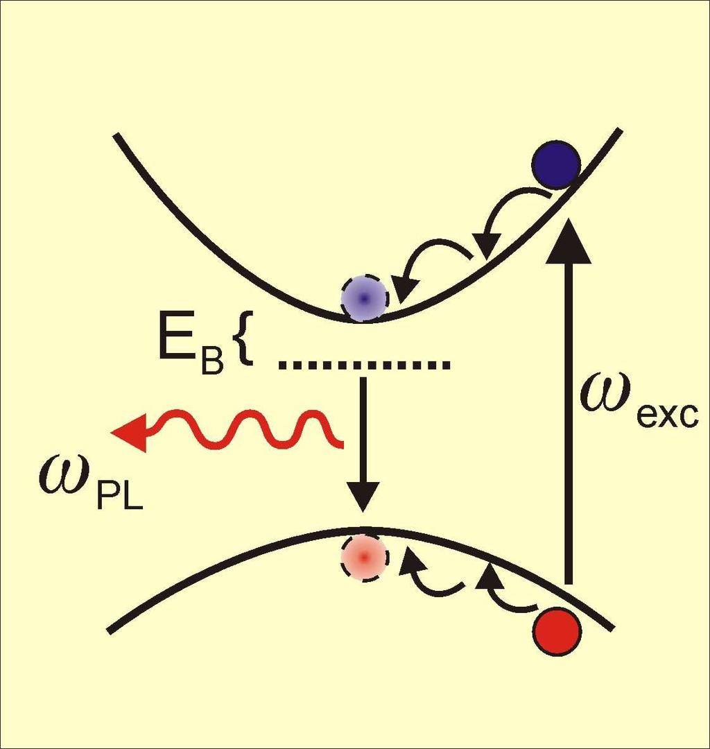
24 Non Resonantly Excited Photoluminescence
25 Experiments? BS non resonant excitation of QW (weak excitation) incoherent (random) emission at exciton resonance different emission directions collected in interferometer setup Path 1 QW Path 2 t measurement combines emission to the left and right directions (less than one photon in interferometer) AP AP control of phase via delay

26 Experiments (I) QW perpendicular BS Path 1 Path 2 QW t AP AP
27 Experiments (II) QW tilted? BS Path 1 Path 2 QW t AP AP

28 Experiments (II) QW tilted BS Path 1 Path 2 QW t AP AP
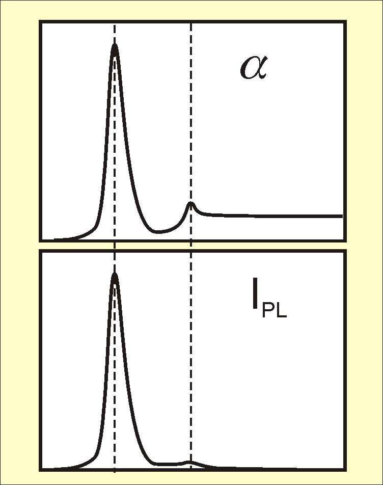
29 Experiments (III) PL intensity (a.u.) Oct with tilt no tilt single beam intensities Contrast t (ps) clear interferences visible if QW NOT tilted interferences vanish if QW tilted CCD pixels Hoyer et al. PRL 93, (2004)
30 Summary of Experimental Observations interferences seen in incoherent (single photon) emission, but intensity shows interferences interference shows strong directional sensitivity
31 Summary of Experimental Observations interferences seen in incoherent (single photon) emission, but intensity shows interferences interference shows strong directional sensitivity effects predicted in Prog. Quantum. El. 23, 189 (1999) origin of effects: light-matter entanglement & which-way interferences
32 Spontaneous Emission from Quantum Wells q q z + q z electron-hole recombination simultaneous emission in and directions photon emission with same recoil momentum transferred to carrier system
33 Explanation of Interferences (I) CASE A: Emission with same q q photon emission to the left many-body wavefunction with recoil emission to the right paths not distinguishable with respect to carrier system (i.e. no entanglement)

34 Explanation of Interferences (II) q q B L B R variable phase interferometry: emission intensity I L to the left I R to the right interference INTERFERENCE can be seen
35 Explanation of Entanglement (I) CASE B: Emission with different photons q q' many-body wavefunction with recoil emission to the left emission to the right paths identified by entanglement

36 Explanation of Entanglement (II) q q' emission to the left (B L ) und to the right (B R ) is combined in detector D = B L +B R emissions intensity I L to the left I R to the right interference NO interference pattern due to entanglement
37 Theory of Entanglement-Interferences semiconductor luminescence equations PRL 97, 5170 (1997) photon-assisted correlations photon correlations in the presence of Coulomb interaction QUESTION: WHAT HAPPENS IF WE TAKE MANY QUANTUM WELLS?
38 Theory of Entanglement-Interferences Predictions for n quantum wells with spacing d perfect interferences for Bragg no interferences for anti-bragg (n-even) Prog. Quantum. El. 23, 189 (1999) /2 /4 1.0 di Number of QWs

39 Entanglement-Interference Experiment (IV) interferences seen in multiple QW system with λ/2 spacing interferences vanish in multiple QW system with λ/4 spacing λ/4 spacing leads to complete randomizing of emission to the left and to the right confirmation of theoretical predictions
40 Summary of Entanglement-Interferences incoherent emission to the left and to the right are entangled with the many-body carrier system emission to the left and to the right with same q is not entangled emission to the left and to the right with same q is entangled description of entanglement via photoncarrier and photon-photon correlations of the type: more in: Hoyer et al. PRL 93, (2004)
41 Summary variety of novel quantum optical effects in semiconductors strong experiment theory interactions MANY CHALLENGES: optimization and application of non-classical properties (quantum information science, ) modified photonic environment (phot. x-tals, ) role of incoherent excitons, biexcitons,. Selected References: Haug/Koch, Quantum Theory of the Optical and Electronic Properties of Semiconductors 4 th ed., World Scientific Publ. (2004) Khitrova et al., Rev. Mod. Phys. 71, 1591 (1999) Kira et al., Prog. Quantum. Electron. 23, 189 (1999)
Microscopic Modelling of the Optical Properties of Quantum-Well Semiconductor Lasers
 Microscopic Modelling of the Optical Properties of Quantum-Well Semiconductor Lasers Stephan W. Koch Department of Physics Philipps University, Marburg/Germany OVERVIEW - Outline of Theory - Gain/Absorption
interband transitions in semiconductors M. Fox, Optical Properties of Solids, Oxford Master Series in Condensed Matter Physics
 interband transitions in semiconductors M. Fox, Optical Properties of Solids, Oxford Master Series in Condensed Matter Physics interband transitions in quantum wells Atomic wavefunction of carriers in
Optical Properties of Solid from DFT
 Optical Properties of Solid from DFT 1 Prof.P. Ravindran, Department of Physics, Central University of Tamil Nadu, India & Center for Materials Science and Nanotechnology, University of Oslo, Norway http://folk.uio.no/ravi/cmt15
Optical Properties of Semiconductors. Prof.P. Ravindran, Department of Physics, Central University of Tamil Nadu, India
 Optical Properties of Semiconductors 1 Prof.P. Ravindran, Department of Physics, Central University of Tamil Nadu, India http://folk.uio.no/ravi/semi2013 Light Matter Interaction Response to external electric
Electronic and Optoelectronic Properties of Semiconductor Structures
 Electronic and Optoelectronic Properties of Semiconductor Structures Jasprit Singh University of Michigan, Ann Arbor CAMBRIDGE UNIVERSITY PRESS CONTENTS PREFACE INTRODUCTION xiii xiv 1.1 SURVEY OF ADVANCES
Luminescence Process
 Luminescence Process The absorption and the emission are related to each other and they are described by two terms which are complex conjugate of each other in the interaction Hamiltonian (H er ). In an
Single Photon Generation & Application
 Single Photon Generation & Application Photon Pair Generation: Parametric down conversion is a non-linear process, where a wave impinging on a nonlinear crystal creates two new light beams obeying energy
Luminescence basics. Slide # 1
 Luminescence basics Types of luminescence Cathodoluminescence: Luminescence due to recombination of EHPs created by energetic electrons. Example: CL mapping system Photoluminescence: Luminescence due to
Optical Properties of Lattice Vibrations
 Optical Properties of Lattice Vibrations For a collection of classical charged Simple Harmonic Oscillators, the dielectric function is given by: Where N i is the number of oscillators with frequency ω
Quantum Theory of the Optical and Electronic Properties of Semiconductors Downloaded from
 This page intentionally left blank Published by World Scientific Publishing Co. Pte. Ltd. 5 Toh Tuck Link, Singapore 596224 USA office: 27 Warren Street, Suite 401-402, Hackensack, NJ 07601 UK office:
Semiconductor-Laser Fundamentals
 Semiconductor-Laser Fundamentals Springer-Verlag Berlin Heidelberg GmbH Weng W. Chow Stephan W. Koch Semiconductor-laser Fundamentals Physics of the Gain Materials With 132 Figures and 3 Tables Springer
Review of Optical Properties of Materials
 Review of Optical Properties of Materials Review of optics Absorption in semiconductors: qualitative discussion Derivation of Optical Absorption Coefficient in Direct Semiconductors Photons When dealing
Exciton spectroscopy
 Lehrstuhl Werkstoffe der Elektrotechnik Exciton spectroscopy in wide bandgap semiconductors Lehrstuhl Werkstoffe der Elektrotechnik (WW6), Universität Erlangen-Nürnberg, Martensstr. 7, 91058 Erlangen Vortrag
Lecture 2. Electron states and optical properties of semiconductor nanostructures
 Lecture Electron states and optical properties of semiconductor nanostructures Bulk semiconductors Band gap E g Band-gap slavery: only light with photon energy equal to band gap can be generated. Very
PHYSICS OF SEMICONDUCTORS AND THEIR HETEROSTRUCTURES
 PHYSICS OF SEMICONDUCTORS AND THEIR HETEROSTRUCTURES Jasprit Singh University of Michigan McGraw-Hill, Inc. New York St. Louis San Francisco Auckland Bogota Caracas Lisbon London Madrid Mexico Milan Montreal
Quantum Condensed Matter Physics Lecture 9
 Quantum Condensed Matter Physics Lecture 9 David Ritchie QCMP Lent/Easter 2018 http://www.sp.phy.cam.ac.uk/drp2/home 9.1 Quantum Condensed Matter Physics 1. Classical and Semi-classical models for electrons
ESE 372 / Spring 2013 / Lecture 5 Metal Oxide Semiconductor Field Effect Transistor
 Metal Oxide Semiconductor Field Effect Transistor V G V G 1 Metal Oxide Semiconductor Field Effect Transistor We will need to understand how this current flows through Si What is electric current? 2 Back
Lecture contents. Burstein shift Excitons Interband transitions in quantum wells Quantum confined Stark effect. NNSE 618 Lecture #15
 1 Lecture contents Burstein shift Excitons Interband transitions in quantum wells Quantum confined Stark effect Absorption edges in semiconductors Offset corresponds to bandgap Abs. coefficient is orders
Polariton Condensation
 Polariton Condensation Marzena Szymanska University of Warwick Windsor 2010 Collaborators Theory J. Keeling P. B. Littlewood F. M. Marchetti Funding from Macroscopic Quantum Coherence Macroscopic Quantum
Metals: the Drude and Sommerfeld models p. 1 Introduction p. 1 What do we know about metals? p. 1 The Drude model p. 2 Assumptions p.
 Metals: the Drude and Sommerfeld models p. 1 Introduction p. 1 What do we know about metals? p. 1 The Drude model p. 2 Assumptions p. 2 The relaxation-time approximation p. 3 The failure of the Drude model
Many-Body Coulomb Effects in the Optical Properties of Semiconductor Heterostructures
 John von Neumann Institute for Computing Many-Body Coulomb Effects in the Optical Properties of Semiconductor Heterostructures Torsten Meier, Bernhard Pasenow, Peter Thomas, Stephan W. Koch published in
Summary lecture VI. with the reduced mass and the dielectric background constant
 Summary lecture VI Excitonic binding energy reads with the reduced mass and the dielectric background constant Δ Statistical operator (density matrix) characterizes quantum systems in a mixed state and
Introduction to Sources: Radiative Processes and Population Inversion in Atoms, Molecules, and Semiconductors Atoms and Molecules
 OPTI 500 DEF, Spring 2012, Lecture 2 Introduction to Sources: Radiative Processes and Population Inversion in Atoms, Molecules, and Semiconductors Atoms and Molecules Energy Levels Every atom or molecule
Electromagnetically Induced Transparency (EIT) via Spin Coherences in Semiconductor
 via Spin Coherences in Semiconductor") Electromagnetically Induced Transparency (EIT) via Spin Coherences in Semiconductor Hailin Wang Oregon Center for Optics, University of Oregon, USA Students: Shannon O Leary Susanta Sarkar Yumin Shen Phedon
Electromagnetically Induced Transparency (EIT) via Spin Coherences in Semiconductor Hailin Wang Oregon Center for Optics, University of Oregon, USA Students: Shannon O Leary Susanta Sarkar Yumin Shen Phedon
Ultrafast Spectroscopy of Semiconductors and Semiconductor Nanostructures
 Springer Series in Solid-State Sciences 115 Ultrafast Spectroscopy of Semiconductors and Semiconductor Nanostructures Bearbeitet von Jagdeep Shah erweitert 1999. Buch. xvi, 522 S. Hardcover ISBN 978 3
Chapter 1 Overview of Semiconductor Materials and Physics
 Chapter 1 Overview of Semiconductor Materials and Physics Professor Paul K. Chu Conductivity / Resistivity of Insulators, Semiconductors, and Conductors Semiconductor Elements Period II III IV V VI 2 B
1 P a g e h t t p s : / / w w w. c i e n o t e s. c o m / Physics (A-level)
") 1 P a g e h t t p s : / / w w w. c i e n o t e s. c o m / Physics (A-level) Electromagnetic induction (Chapter 23): For a straight wire, the induced current or e.m.f. depends on: The magnitude of the magnetic
1 P a g e h t t p s : / / w w w. c i e n o t e s. c o m / Physics (A-level) Electromagnetic induction (Chapter 23): For a straight wire, the induced current or e.m.f. depends on: The magnitude of the magnetic
Lecture 3: Optical Properties of Insulators, Semiconductors, and Metals. 5 nm
 Metals Lecture 3: Optical Properties of Insulators, Semiconductors, and Metals 5 nm Course Info Next Week (Sept. 5 and 7) no classes First H/W is due Sept. 1 The Previous Lecture Origin frequency dependence
OPTICAL PROPERTIES of Nanomaterials
 OPTICAL PROPERTIES of Nanomaterials Advanced Reading Optical Properties and Spectroscopy of Nanomaterials Jin Zhong Zhang World Scientific, Singapore, 2009. Optical Properties Many of the optical properties
Bohr s Model, Energy Bands, Electrons and Holes
 Dual Character of Material Particles Experimental physics before 1900 demonstrated that most of the physical phenomena can be explained by Newton's equation of motion of material particles or bodies and
Basic cell design. Si cell
 Basic cell design Si cell 1 Concepts needed to describe photovoltaic device 1. energy bands in semiconductors: from bonds to bands 2. free carriers: holes and electrons, doping 3. electron and hole current:
SUPPLEMENTARY INFORMATION
 Sub-cycle control of terahertz high-harmonic generation by dynamical Bloch oscillations O. Schubert 1, M. Hohenleutner 1, F. Langer 1, B. Urbanek 1, C. Lange 1, U. Huttner 2, D. Golde 2, T. Meier 3, M.
Chapter 5. Semiconductor Laser
 Chapter 5 Semiconductor Laser 5.0 Introduction Laser is an acronym for light amplification by stimulated emission of radiation. Albert Einstein in 1917 showed that the process of stimulated emission must
Review of Semiconductor Physics
 Solid-state physics Review of Semiconductor Physics The daunting task of solid state physics Quantum mechanics gives us the fundamental equation The equation is only analytically solvable for a handful
M R S Internet Journal of Nitride Semiconductor Research
 M R S Internet Journal of Nitride Semiconductor Research Volume 2, Article 25 Properties of the Biexciton and the Electron-Hole-Plasma in Highly Excited GaN J.-Chr. Holst, L. Eckey, A. Hoffmann, I. Broser
Chapter 3 Properties of Nanostructures
 Chapter 3 Properties of Nanostructures In Chapter 2, the reduction of the extent of a solid in one or more dimensions was shown to lead to a dramatic alteration of the overall behavior of the solids. Generally,
A. F. J. Levi 1 EE539: Engineering Quantum Mechanics. Fall 2017.
 A. F. J. Levi 1 Engineering Quantum Mechanics. Fall 2017. TTh 9.00 a.m. 10.50 a.m., VHE 210. Web site: http://alevi.usc.edu Web site: http://classes.usc.edu/term-20173/classes/ee EE539: Abstract and Prerequisites
Physics and Material Science of Semiconductor Nanostructures
 Physics and Material Science of Semiconductor Nanostructures PHYS 570P Prof. Oana Malis Email: omalis@purdue.edu Course website: http://www.physics.purdue.edu/academic_programs/courses/phys570p/ 1 Introduction
Lecture 15: Optoelectronic devices: Introduction
 Lecture 15: Optoelectronic devices: Introduction Contents 1 Optical absorption 1 1.1 Absorption coefficient....................... 2 2 Optical recombination 5 3 Recombination and carrier lifetime 6 3.1
Semiconductor Physics and Devices Chapter 3.
 Introduction to the Quantum Theory of Solids We applied quantum mechanics and Schrödinger s equation to determine the behavior of electrons in a potential. Important findings Semiconductor Physics and
Laser Diodes. Revised: 3/14/14 14: , Henry Zmuda Set 6a Laser Diodes 1
 Laser Diodes Revised: 3/14/14 14:03 2014, Henry Zmuda Set 6a Laser Diodes 1 Semiconductor Lasers The simplest laser of all. 2014, Henry Zmuda Set 6a Laser Diodes 2 Semiconductor Lasers 1. Homojunction
Chapter 2 Optical Transitions
 Chapter 2 Optical Transitions 2.1 Introduction Among energy states, the state with the lowest energy is most stable. Therefore, the electrons in semiconductors tend to stay in low energy states. If they
ISSN: [bhardwaj* et al., 5(11): November, 2016] Impact Factor: 4.116
![ISSN: [bhardwaj* et al., 5(11): November, 2016] Impact Factor: 4.116](/thumbs/87/97249459.jpg "ISSN: [bhardwaj* et al., 5(11): November, 2016] Impact Factor: 4.116") ISSN: 77-9655 [bhardwaj* et al., 5(11): November, 016] Impact Factor: 4.116 IJESRT INTERNATIONAL JOURNAL OF ENGINEERING SCIENCES & RESEARCH TECHNOLOGY EXCITON BINDING ENERGY IN BULK AND QUANTUM WELL OF
ISSN: 77-9655 [bhardwaj* et al., 5(11): November, 016] Impact Factor: 4.116 IJESRT INTERNATIONAL JOURNAL OF ENGINEERING SCIENCES & RESEARCH TECHNOLOGY EXCITON BINDING ENERGY IN BULK AND QUANTUM WELL OF
Self-Assembled InAs Quantum Dots
 Self-Assembled InAs Quantum Dots Steve Lyon Department of Electrical Engineering What are semiconductors What are semiconductor quantum dots How do we make (grow) InAs dots What are some of the properties
Nanomaterials and their Optical Applications
 Nanomaterials and their Optical Applications Winter Semester 2013 Lecture 02 rachel.grange@uni-jena.de http://www.iap.uni-jena.de/multiphoton Lecture 2: outline 2 Introduction to Nanophotonics Theoretical
SUPPLEMENTARY INFORMATION
 doi:10.1038/nature12036 We provide in the following additional experimental data and details on our demonstration of an electrically pumped exciton-polariton laser by supplementing optical and electrical
Intensity / a.u. 2 theta / deg. MAPbI 3. 1:1 MaPbI 3-x. Cl x 3:1. Supplementary figures
 Intensity / a.u. Supplementary figures 110 MAPbI 3 1:1 MaPbI 3-x Cl x 3:1 220 330 0 10 15 20 25 30 35 40 45 2 theta / deg Supplementary Fig. 1 X-ray Diffraction (XRD) patterns of MAPbI3 and MAPbI 3-x Cl
Course overview. Me: Dr Luke Wilson. The course: Physics and applications of semiconductors. Office: E17 open door policy
 Course overview Me: Dr Luke Wilson Office: E17 open door policy email: luke.wilson@sheffield.ac.uk The course: Physics and applications of semiconductors 10 lectures aim is to allow time for at least one
Metal Vapour Lasers Use vapoured metal as a gain medium Developed by W. Silfvast (1966) Two types: Ionized Metal vapour (He-Cd) Neutral Metal vapour
 Two types: Ionized Metal vapour (He-Cd) Neutral Metal vapour") Metal Vapour Lasers Use vapoured metal as a gain medium Developed by W. Silfvast (1966) Two types: Ionized Metal vapour (He-Cd) Neutral Metal vapour (Cu) All operate by vaporizing metal in container Helium
Metal Vapour Lasers Use vapoured metal as a gain medium Developed by W. Silfvast (1966) Two types: Ionized Metal vapour (He-Cd) Neutral Metal vapour (Cu) All operate by vaporizing metal in container Helium
Lecture 21: Lasers, Schrödinger s Cat, Atoms, Molecules, Solids, etc. Review and Examples. Lecture 21, p 1
 Lecture 21: Lasers, Schrödinger s Cat, Atoms, Molecules, Solids, etc. Review and Examples Lecture 21, p 1 Act 1 The Pauli exclusion principle applies to all fermions in all situations (not just to electrons
Magnetostatic modulation of nonlinear refractive index and absorption in quantum wires
 Superlattices and Microstructures, Vol. 23, No. 6, 998 Article No. sm96258 Magnetostatic modulation of nonlinear refractive index and absorption in quantum wires A. BALANDIN, S.BANDYOPADHYAY Department
g-factors in quantum dots
 g-factors in quantum dots Craig Pryor Dept. of Physics and Astronomy University of Iowa With: Michael Flatté, Joseph Pingenot, Amrit De supported by DARPA/ARO DAAD19-01-1-0490 g-factors in quantum dots
GeSi Quantum Dot Superlattices
 GeSi Quantum Dot Superlattices ECE440 Nanoelectronics Zheng Yang Department of Electrical & Computer Engineering University of Illinois at Chicago Nanostructures & Dimensionality Bulk Quantum Walls Quantum
Part I. Nanostructure design and structural properties of epitaxially grown quantum dots and nanowires
 Part I Nanostructure design and structural properties of epitaxially grown quantum dots and nanowires 1 Growth of III V semiconductor quantum dots C. Schneider, S. Höfling and A. Forchel 1.1 Introduction
Confocal Microscopy Imaging of Single Emitter Fluorescence and Hanbury Brown and Twiss Photon Antibunching Setup
 1 Confocal Microscopy Imaging of Single Emitter Fluorescence and Hanbury Brown and Twiss Photon Antibunching Setup Abstract Jacob Begis The purpose of this lab was to prove that a source of light can be
Optical Characterization of Solids
 D. Dragoman M. Dragoman Optical Characterization of Solids With 184 Figures Springer 1. Elementary Excitations in Solids 1 1.1 Energy Band Structure in Crystalline Materials 2 1.2 k p Method 11 1.3 Numerical
Deterministic Coherent Writing and Control of the Dark Exciton Spin using Short Single Optical Pulses
 Deterministic Coherent Writing and Control of the Dark Exciton Spin using Short Single Optical Pulses Ido Schwartz, Dan Cogan, Emma Schmidgall, Liron Gantz, Yaroslav Don and David Gershoni The Physics
Investigation on Mode Splitting and Degeneracy in the L3 Photonic Crystal Nanocavity via Unsymmetrical Displacement of Air-Holes
 The International Journal Of Engineering And Science (Ijes) Volume 2 Issue 2 Pages 146-150 2013 Issn: 2319 1813 Isbn: 2319 1805 Investigation on Mode Splitting and Degeneracy in the L3 Photonic Crystal
Zero- or two-dimensional?
 Stacked layers of submonolayer InAs in GaAs: Zero- or two-dimensional? S. Harrison*, M. Young, M. Hayne, P. D. Hodgson, R. J. Young A. Schliwa, A. Strittmatter, A. Lenz, H. Eisele, U. W. Pohl, D. Bimberg
(002)(110) (004)(220) (222) (112) (211) (202) (200) * * 2θ (degree)
(110) (004)(220) (222) (112) (211) (202) (200) * * 2θ (degree)") Supplementary Figures. (002)(110) Tetragonal I4/mcm Intensity (a.u) (004)(220) 10 (112) (211) (202) 20 Supplementary Figure 1. X-ray diffraction (XRD) pattern of the sample. The XRD characterization indicates
Supplementary Figures. (002)(110) Tetragonal I4/mcm Intensity (a.u) (004)(220) 10 (112) (211) (202) 20 Supplementary Figure 1. X-ray diffraction (XRD) pattern of the sample. The XRD characterization indicates
Fall 2014 Nobby Kobayashi (Based on the notes by E.D.H Green and E.L Allen, SJSU) 1.0 Learning Objectives
 1.0 Learning Objectives") University of California at Santa Cruz Electrical Engineering Department EE-145L: Properties of Materials Laboratory Lab 7: Optical Absorption, Photoluminescence Fall 2014 Nobby Kobayashi (Based on the
University of California at Santa Cruz Electrical Engineering Department EE-145L: Properties of Materials Laboratory Lab 7: Optical Absorption, Photoluminescence Fall 2014 Nobby Kobayashi (Based on the
When I hear of Schrödinger s cat, I reach for my gun. --Stephen W. Hawking. Lecture 21, p 1
 When I hear of Schrödinger s cat, I reach for my gun. --Stephen W. Hawking Lecture 21, p 1 Lecture 21: Lasers, Schrödinger s Cat, Atoms, Molecules, Solids, etc. Review and Examples Lecture 21, p 2 Act
1 Review of semiconductor materials and physics
 Part One Devices 1 Review of semiconductor materials and physics 1.1 Executive summary Semiconductor devices are fabricated using specific materials that offer the desired physical properties. There are
OPTICAL PROPERTIES AND SPECTROSCOPY OF NANOAAATERIALS. Jin Zhong Zhang. World Scientific TECHNISCHE INFORMATIONSBIBLIOTHEK
 OPTICAL PROPERTIES AND SPECTROSCOPY OF NANOAAATERIALS Jin Zhong Zhang University of California, Santa Cruz, USA TECHNISCHE INFORMATIONSBIBLIOTHEK Y World Scientific NEW JERSEY. t'on.don SINGAPORE «'BEIJING
Summary lecture VII. Boltzmann scattering equation reads in second-order Born-Markov approximation
 Summary lecture VII Boltzmann scattering equation reads in second-order Born-Markov approximation and describes time- and momentum-resolved electron scattering dynamics in non-equilibrium Markov approximation
Signal regeneration - optical amplifiers
 Signal regeneration - optical amplifiers In any atom or solid, the state of the electrons can change by: 1) Stimulated absorption - in the presence of a light wave, a photon is absorbed, the electron is
Summary lecture IX. The electron-light Hamilton operator reads in second quantization
 Summary lecture IX The electron-light Hamilton operator reads in second quantization Absorption coefficient α(ω) is given by the optical susceptibility Χ(ω) that is determined by microscopic polarization
Distribution of Delay Times in Laser Excited CdSe-ZnS Core-Shell Quantum Dots
 Distribution of Delay Times in Laser Excited CdSe-ZnS Core-Shell Quantum Dots Andrei Vajiac Indiana University South Bend Mathematics, Computer Science Advisor: Pavel Frantsuzov, Physics Abstract This
QUANTUM WELL OPTICAL SWITCHING DEVICES. DAVID A. B. MILLER Rm. 4B-401, AT&T Bell Laboratories Holmdel, NJ USA
 QUANTUM WELL OPTICAL SWITCHING DEVICES DAVID A. B. MILLER Rm. 4B-401, AT&T Bell Laboratories Holmdel, NJ07733-3030 USA ABSTRACT These lecture notes summarize the basic physics of quantum wells for optical
Charge Excitation. Lecture 4 9/20/2011 MIT Fundamentals of Photovoltaics 2.626/2.627 Fall 2011 Prof. Tonio Buonassisi
 Charge Excitation Lecture 4 9/20/2011 MIT Fundamentals of Photovoltaics 2.626/2.627 Fall 2011 Prof. Tonio Buonassisi 1 2.626/2.627 Roadmap You Are Here 2 2.626/2.627: Fundamentals Every photovoltaic device
Lecture 2: Background dconcepts
 Optoelectronics I Lecture : Background dconcepts M. Soroosh Assistant Professor of Electronics Shahid Chamran University 1 Face Centered Crystal (FCC) Body Centered Crystal (BCC) Bragg s Law William Lawrence
Single-photon nonlinearity of a semiconductor quantum dot in a cavity
 Single-photon nonlinearity of a semiconductor quantum dot in a cavity D. Sanvitto, F. P. Laussy, F. Bello, D. M. Whittaker, A. M. Fox and M. S. Skolnick Department of Physics and Astronomy, University
Opto-electronic Characterization of Perovskite Thin Films & Solar Cells
 Opto-electronic Characterization of Perovskite Thin Films & Solar Cells Arman Mahboubi Soufiani Supervisors: Prof. Martin Green Prof. Gavin Conibeer Dr. Anita Ho-Baillie Dr. Murad Tayebjee 22 nd June 2017
Lasers. Stimulated Emission Lasers: Trapping Photons Terahertz Lasers Course Overview
 Lasers Stimulated Emission Lasers: Trapping Photons Terahertz Lasers Course Overview 1 P-N Junctions and LEDs Terminal Pins Emitted Light Beams Diode Transparent Plastic Case High energy electrons (n-type)
Quantum Theory of the Semiconductor Luminescence
 F. Jahnke, M. Kira and S.W. Koch Quantum Theory of the Semiconductor Luminescence Abstract A fully quantum mechanical theory for the interaction of light and electron-hole excitations in semiconductor
Fluorescence Spectroscopy
 Fluorescence Spectroscopy Frequency and time dependent emission Emission and Excitation fluorescence spectra Stokes Shift: influence of molecular vibrations and solvent Time resolved fluorescence measurements
PH575 Spring Lecture #20 Semiconductors: optical properties: Kittel Ch. 8 pp ; Ch 15 pp
 PH575 Spring 2014 Lecture #20 Semiconductors: optical properties: Kittel Ch. 8 pp. 187-191; Ch 15 pp. 435-444 Figure VI-1-1: Different types of optical absorption phenomena; (1) transitions of highlying
Lecture 20: Semiconductor Structures Kittel Ch 17, p , extra material in the class notes
 Lecture 20: Semiconductor Structures Kittel Ch 17, p 494-503, 507-511 + extra material in the class notes MOS Structure Layer Structure metal Oxide insulator Semiconductor Semiconductor Large-gap Semiconductor
Magneto-Optical Properties of Quantum Nanostructures
 Magneto-optics of nanostructures Magneto-Optical Properties of Quantum Nanostructures Milan Orlita Institute of Physics, Charles University Institute of Physics, Academy of Sciences of the Czech Republic
Direct and Indirect Semiconductor
 Direct and Indirect Semiconductor Allowed values of energy can be plotted vs. the propagation constant, k. Since the periodicity of most lattices is different in various direction, the E-k diagram must
Simple strategy for enhancing terahertz emission from coherent longitudinal optical phonons using undoped GaAs/n-type GaAs epitaxial layer structures
 Presented at ISCS21 June 4, 21 Session # FrP3 Simple strategy for enhancing terahertz emission from coherent longitudinal optical phonons using undoped GaAs/n-type GaAs epitaxial layer structures Hideo
Temperature Dependent Optical Band Gap Measurements of III-V films by Low Temperature Photoluminescence Spectroscopy
 Temperature Dependent Optical Band Gap Measurements of III-V films by Low Temperature Photoluminescence Spectroscopy Linda M. Casson, Francis Ndi and Eric Teboul HORIBA Scientific, 3880 Park Avenue, Edison,
Last Lecture. Overview and Introduction. 1. Basic optics and spectroscopy. 2. Lasers. 3. Ultrafast lasers and nonlinear optics
 Last Lecture Overview and Introduction 1. Basic optics and spectroscopy. Lasers 3. Ultrafast lasers and nonlinear optics 4. Time-resolved spectroscopy techniques Jigang Wang, Feb, 009 Today 1. Spectroscopy
arxiv: v2 [cond-mat.mes-hall] 6 Apr 2011
![arxiv: v2 [cond-mat.mes-hall] 6 Apr 2011](/thumbs/72/66469363.jpg "arxiv: v2 [cond-mat.mes-hall] 6 Apr 2011") Electron spin relaxation as evidence of excitons in a two dimensional electron-hole plasma arxiv:1103.2474v2 [cond-mat.mes-hall] 6 Apr 2011 S. Oertel, 1 S. Kunz, 1 D. Schuh, 2 W. Wegscheider, 3 J. Hübner,
Electron spin relaxation as evidence of excitons in a two dimensional electron-hole plasma arxiv:1103.2474v2 [cond-mat.mes-hall] 6 Apr 2011 S. Oertel, 1 S. Kunz, 1 D. Schuh, 2 W. Wegscheider, 3 J. Hübner,
Introduction to Optoelectronic Device Simulation by Joachim Piprek
 NUSOD 5 Tutorial MA Introduction to Optoelectronic Device Simulation by Joachim Piprek Outline:. Introduction: VCSEL Example. Electron Energy Bands 3. Drift-Diffusion Model 4. Thermal Model 5. Gain/Absorption
Quantum Computing with neutral atoms and artificial ions
 Quantum Computing with neutral atoms and artificial ions NIST, Gaithersburg: Carl Williams Paul Julienne T. C. Quantum Optics Group, Innsbruck: Peter Zoller Andrew Daley Uwe Dorner Peter Fedichev Peter
2.57/2.570 Midterm Exam No. 1 April 4, :00 am -12:30 pm
 Name:.57/.570 Midterm Exam No. April 4, 0 :00 am -:30 pm Instructions: ().57 students: try all problems ().570 students: Problem plus one of two long problems. You can also do both long problems, and one
Solar Cell Materials and Device Characterization
 Solar Cell Materials and Device Characterization April 3, 2012 The University of Toledo, Department of Physics and Astronomy SSARE, PVIC Principles and Varieties of Solar Energy (PHYS 4400) and Fundamentals
Multilevel Infrared Coupling of Excitons in Quantum-Well Semiconductors
 IEEE JOURNAL OF QUANTUM ELECTRONICS, VOL. 36, NO. 11, NOVEMBER 2000 1267 Multilevel Infrared Coupling of Excitons in Quantum-Well Semiconductors S. M. Sadeghi, J. Meyer, T. Tiedje, and M. Beaudoin Abstract
Optical Spectroscopy of Advanced Materials
 Phys 590B Condensed Matter Physics: Experimental Methods Optical Spectroscopy of Advanced Materials Basic optics, nonlinear and ultrafast optics Jigang Wang Department of Physics, Iowa State University
Lecture 0. NC State University
 Chemistry 736 Lecture 0 Overview NC State University Overview of Spectroscopy Electronic states and energies Transitions between states Absorption and emission Electronic spectroscopy Instrumentation Concepts
what happens if we make materials smaller?
 what happens if we make materials smaller? IAP VI/10 ummer chool 2007 Couvin Prof. ns outline Introduction making materials smaller? ynthesis how do you make nanomaterials? Properties why would you make
Dr. Masahiro Yoshita Inst. for Sol. St. Physics Univ. of Tokyo CREST, JST Kashiwanoha, Kashiwa Chiba , JAPAN. Dear Dr.
 Subject: Your_manuscript LP9512 Yoshita From: Physical Review Letters Date: Tue, 13 Jul 2004 18:56:22 UT To: yoshita@issp.u-tokyo.ac.jp Re: LP9512 Crossover of excitons to an electron-hole
Three-Dimensional Silicon-Germanium Nanostructures for Light Emitters and On-Chip Optical. Interconnects
 Three-Dimensional Silicon-Germanium Nanostructures for Light Emitters and On-Chip Optical eptember 2011 Interconnects Leonid Tsybeskov Department of Electrical and Computer Engineering New Jersey Institute
Light Interaction with Small Structures
 Light Interaction with Small Structures Molecules Light scattering due to harmonically driven dipole oscillator Nanoparticles Insulators Rayleigh Scattering (blue sky) Semiconductors...Resonance absorption
3.15 Electrical, Optical, and Magnetic Materials and Devices Caroline A. Ross Fall Term, 2005
 3.15 Electrical, Optical, and Magnetic Materials and Devices Caroline A. Ross Fall Term, 2005 Exam 2 (5 pages) Closed book exam. Formulae and data are on the last 3.5 pages of the exam. This takes 80 min
Engineering 2000 Chapter 8 Semiconductors. ENG2000: R.I. Hornsey Semi: 1
 Engineering 2000 Chapter 8 Semiconductors ENG2000: R.I. Hornsey Semi: 1 Overview We need to know the electrical properties of Si To do this, we must also draw on some of the physical properties and we
Condensed matter physics FKA091
 Condensed matter physics FKA091 Ermin Malic Department of Physics Chalmers University of Technology Henrik Johannesson Department of Physics University of Gothenburg Teaching assistants: Roland Jago &
January 2010, Maynooth. Photons. Myungshik Kim.
 January 2010, Maynooth Photons Myungshik Kim http://www.qteq.info Contents Einstein 1905 Einstein 1917 Hanbury Brown and Twiss Light quanta In 1900, Max Planck was working on black-body radiation and suggested
How to measure packaging-induced strain in high-brightness diode lasers?
 How to measure packaging-induced strain in high-brightness diode lasers? Jens W. Tomm Max-Born-Institut für Nichtlineare Optik und Kurzzeitspektroskopie Berlin Max-Born-Str. 2 A, D-12489 Berlin, Germany