Reduced graphene oxide as ultra fast temperature sensor
|
|
|
- Megan McKinney
- 5 years ago
- Views:
Transcription
1 Reduced graphene oxide as ultra fast temperature sensor Satyaprakash Sahoo, *,1 Sujit K. Barik, 1 G. L. Sharma, 1 Geetika Khurana, 1 J. F. Scott 2 and Ram S. Katiyar 1 1Department of Physics, University of Puerto Rico, San Juan, USA 2 Department of Physics, Cavendish Laboratory, University of Cambridge, Cambridge, CB3 0HE, United Kingdom We demonstrate the excellent temperature sensing property of a chemically synthesized reduced graphene oxide (rgo). It is found that with increase in temperature from 80 to 375K, the resistivity of reduced graphene oxide monotonically decreases. The ultra-fast temperature sensing property is demonstrated by keeping and removing a block of ice under the rgo sensor, which shows the resistance of rgo increases by 15% in 592 miliseconds and recovers in 8.92 seconds. The temperature sensing of rgo is compared with a standard platinum thermo sensor (Pt 111) and found the sensitivity is much better in rgo. * Corresponding Author: satya504@gmail.com 1
2 In recent years graphene has gained a tremendous research interest due to its unusual physical properties such as high carrier mobility, quantum Hall effect, high electrical and thermal conductivity etc. 1-5 The charge carriers in graphene are mass less Dirac fermions. Graphene is the basic building block of carbon nanotube, fullerene and graphite. On the other hand, graphene oxide is a derivative of graphene in which most of the pi-bonds between carbon-carbon atoms are shared either by oxygen or functional hydroxyl group. 6 Thus both graphene and graphene oxide share the same crystallographic atomic layered structure. However, the presence of oxygen and hydroxyl groups make graphene oxide more resistive to electric field than that of graphene. The reduction of graphene oxide can be achieved under harassing reducing environments using hydrazin or high temperature treatment and the electrical conductivity can significantly be tuned. The advantage of GO over graphene is mainly due to the fact that the former can be produced easily and in large quantities. Secondly, GO is usually dispersed as single sheet in water and hence a continuous film of GO can easily be prepared on a substrate. 7 The reduced graphene oxide (rgo) has shown many promising applications such as gas sensor, field effect transistor, bio-sensor, etc Being atomically thin and having a high surface-to-volume ratio, its surface can absorb gas molecules very efficiently. Although there are many reports on the gas sensing properties of GO, its temperature sensing properties have not been reported so far. Here we report the temperature sensing properties of rgo over a wide temperature range (375 K 80 K) and demonstrate the ultra fast sensing properties using an ice cube. Graphene oxide (GO) synthesis was performed using a modified Hummers method. 13 Concentrated H 2 SO 4 was added to highly oriented pyrolytic graphite (HOPG, 2g) in a at room temperature followed by continuous stirring using magnetic stirrer. The flask was kept in an ice bath to maintain a constant low reaction temperature. Potassium permanganate (KMnO 4, 7g) was 2
3 added very slowly to the solution. After that excess of distilled water was added slowly to the solution. Hydrogen peroxide was added slowly while stirring until the gas evolution stopped. The resultant mixture filtered using a vacuum glass filter and the precipitates obtained were dried for 24 hours in a vacuum oven at room temperature. In the present study the exfoliation of the GO sheets was performed in this manner by sonicating the graphite oxide in water for 2 hours. The sensor device was fabricated by drop casting the GO solution directly on the platinum interdigital electrodes (Pt-IDE) and was allowed to dry and then heated at about 400 O C for few minutes then followed by hydrazin vapor treatment. It may be noted that the resistance of the GO before annealing was about few mega-ohms but changes to several ohms after reduction. The platinum electrodes were made out of Pt metal on a thin (1 mm) Al 2 O 3 substrate using electron beam lithography. A thinner substrate was used to ensure quick thermal equilibrium between the sensor and the environment. The temperature dependent resistance was measured using a MMR temperature controller (K-20) and Keithley 2401 meter. The sensing properties of rgo were measured using a Keithley 2401 meter. Figure 1 shows the optical image of the rgo layer on the Pt-IDE. It shows that the rgo evenly covers the electrodes except for few places, where some tearing and subsequent folding of rgo is observed. Figure 2(a) is the FESEM image of the Pt-IDE on which few layers of GO were deposited. Each of the Pt-IDE electrodes is 1000 and 20 µm in length and width, respectively. The spacing between the consecutive electrode fingers is about 20 µm. FESEM image of the several-layer rgo film on the Pt-IDE is shown in Fig. 2 (b), (c), and (d). The rgo film is vey transparent, as can be seen from the high magnifying images [Fig. 2 (c) and (d)], which indicates that our rgo sheets are very thin and may be consisting of only a few layers of rgo. Figure 3 compares the Raman spectra of GO to that of rgo. Both GO and rgo have two 3
4 distinct peaks: Those at 1350 and 1580 cm -1 are the so-called D and G Raman bands, respectively. 14 The peak height of D and G are almost the same in GO. However, the D band intensity is larger than that of G in rgo, and this is due to the formation of large number of defects during reduction process. The Raman spectra of GO and rgo are consistent with other reported results. 15 We fabricated many rgo sheets of different electrical resistance to study the sensing properties. Next, we will show the temperature sensing properties of two rgo sheets. Figure 4 shows the current (I) verses voltage (V) plot of sample 1 at T = 375K and 80 K. It is found that the current increases linearly with increasing voltage from -1 V to +1 V. The linear I-V characteristic indicates the ohmic nature of rgo. Although the I-V plot shows ohmic nature for other temperatures between 375 K and 80 K, we have not shown them here for clarity. Hence, we have used the Ohm s law to calculate the resistance (R = V/I) of the rgo sheets in the measured temperature range. Samples of deferent resistances show similar behavior. It is worth to mention here that a non-linear IV curve can be obtained, if the GO is not reduced enough. 16 Figure 5 shows the temperature dependence of the resistance R(T) of rgo sensor. It is found that the resistance decreases almost linearly with increase in temperature in the measured temperature region 80 to 375 K, which shows the behavior of an intrinsic semiconductor. A similar temperature dependent resistance behavior has been reported in metallic carbon nanotube and monolayer and bilayer graphene. 17,18 Uher et al. 19 have reported such unusual temperature dependent resistance in exfoliated graphite and according to them the negative coefficient of resistivity is some form of activated behavior and not intrinsic to graphites rather related to high density of defects. However, the exact mechanism is still not clear. It is important to know the coefficient of resistance (α) of rgo temperature sensor for its sensor characteristic. Hence, we 4
5 have calculated α for rgo from the above results using the expression, α=(1/r 0 ) (dr/dt), where R 0 is the resistance of the sample at 273 K and dr/dt is the slope of the R-T curve. We have fitted the resistance behavior in the entire temperature region using a linear equation and the slope is found to be Ohm/K. As the value of R 0 is 554 Ω at 273 K, the α is found to be K -1 which is one order larger than that of reported carbon nanotube. 17 This experiment was performed several times and over several periods of times to ensure repeatability of the result. The temperature sensing performance test was conducted by keeping the rgo sensor device on a block of ice. A constant voltage of 1V was applied across the two terminals of the device and the change in current/resistance was monitored by periodically touching and removing the ice block. The ice was in full physical contact with the back side of the device to ensure proper thermal equilibrium between the ice and the sample. The thin substrate also helps in quick thermal equilibrium. We have performed the temperature sensing in two rgo devices with different room temperature resistances; sample 1 (240 ohm), sample 2 (520 ohm). Figure 6 shows the resistance verses time graph of sample 1 and sample 2. When the sample was just touched to the ice block, the resistance increases abruptly and almost saturates after few millisecond. Once the ice is removed the resistance drops exponentially and reaches room temperature resistance. It is found that while the resistance increases by 15% in sample 2, it increases by 12% in sample 1 upon touching the ice block with the sensor. As can be seen from the graph that response time is much faster than the recovery time which a characteristic of sensor. We calculate the recovery time for both the sensors by fitting the graphs using the following simplified equation, R(t)=R 0 +A exp[-(t-b)/ τ], (1) 5
6 where R 0 is the room temperature resistance, A is the amplitude, B is a constant and ζ is the recovery/response time. The fitted curve is shown in Fig. 7 (a). The recovery times (τ r ) were found to be around 6.35 and 8.19 seconds for sample 1 and sample 2, respectively. The response times (τ s ) were also calculated from the plot and are found to be 0.58 and 0.59 seconds for sample 1 and sample 2, respectively. The temperature sensitivity of rgo sensor was also compared with that of standard platinum sensor (Pt 111) (see Fig. 7(b)) by using the similar experimental set up. Both the response and recovery times in Pt 111 are found to be much slower than that of the rgo sensor for same change in temperature (297 to 273K). The response and recovery times of Pt 111 were calculated to be 8.66 and seconds, respectively and the change is resistance is also smaller (~ 6.8%). Note that, while the resistance of Pt 111 sensor decreases with decreasing temperature, the resistance increases with decreasing temperature of rgo. In summary the temperature sensing effect in film of reduced graphene oxide a few layers thick has been studied. The linearity in resistance as a function of temperature is verified over a wide range of temperature (from 80 to 375K). The temperature sensitivity is found to be much faster than the standard platinum thermometer. The response and recovery times of rgo are 8 and 3 times faster than that of PT-111 sensor in the temperature range of 297 to 273K. Thus rgo could be a potential candidate as a fast temperature sensor. Acknowledgements: The authors acknowledge partial financial support from DoE through Grant No. DE-FG02-ER
7 References 1. K. S. Novoselov, A.K. Geim, S. V. Morozov, D. Jiang, Y. Zhang, S.V. Dubonos, I. V. Grigorieva, A. A. Firsov, Science 306, 666 (2004). 2. Y. Zhang, Y. -W. Tan, H. L. Stormer, P.Kim, Nature 438, 201 (2005). 3. K. S. Novoselov, Z. Jiang, Y. Zhang, S. V. Morozov, H. L. Stormer, U. Zeitler, J. C. Maan, G. S. Boebinger, P. Kim, A. K. Geim, Science 315, 1379 (2007). 4. A. K. Geim, and K. S. Novoselov, Nature Materials 6, 183 (2007). 5. A. A. Balandin, S. Ghosh, W. Bao, I. Calizo, D. Teweldebrhan, F. Miao, C. N. Lau, Nano Lett. 8, 902 (2008). 6. D. R. Dreyer, S. Park, C. W. Bielawski, R. S. Ruoff, Chem. Soc. Rev. 39, 228 (2010). 7. Y. Si, E. T. Samulski, Nano Lett. 8, 1679 (2008). 8. J. T. Robinson, F. K. Perkins, E. S. Snow, Z. Wei, P. E. Sheehan, Nano Lett., 8, 3137 (2008). 9. G. Lu, L. E. Ocola, J. Chen, Appl. Phys. Lett. 94, (2009). 10. S. Wang, P. K. Ang, Z. Wang, A. L. L. Tang, J. T. L. Thong, K. P. Loh, Nano Lett., 10, 92 (2010). 11. S. Mao, G. Lu, K. Yu, Z. Bo, J. Chen, Adv. Mat., 22, 3521 (2010). 12. Y. Liu, D. Yu, C. Zeng, Z. Miao, L. Dai, Langmuir, 26, 6158 (2010). 13. W. S. Hummers, R. E. Offeman, J. Am. Chem. Soc. 80, 1339 (1958). 14. K. N. Kudin, B. Ozbas, H. C. Schniepp, R. K. Prud'homme, I. A. Aksay, R. Car, Nano Lett., 8, 36, (2008). 15. I. K. Moon, J. Lee, R. S. Ruoff, H. Lee, Nat. Commun., 1, 73, (2010). 16. I. Jung, D. A. Dikin, R. D. Piner, R. S. Ruoff, Nano Lett., 8, 4283, (2008). 7
8 17. A. D. Bartolomeo, M. Sarno, F. Giubileo, C. Altavilla, L. Iemmo, S. Piano, F. Bobba, M. Longobardi, A. Scarfato, D. Sannino, A. M. Cucolo, P. Ciambelli, J. Appl. Phys., 105, (2009). 18. Q. Shao, G. Liu, D. Teweldebrhan, A. A. Balandinm, Appl. Phys. Lett., 92, , (2008). 19. C. Uher, L. M. Sander, Phys. Rev. B., 27, 1326 (1983). 8
9 Figure Captions Fig. 1. Optical microscopy image of rgo film on Pt-IDE. Fig. 2. (a) FESEM image of a Pt-IDE. (b), (c) and (d) FESEM image of few layer reduced graphene oxide with different magnifications. Fig. 3. Comparison of Raman spectra of graphene oxide and reduced graphene oxide. Fig. 4. Current verses voltage graph of rgo thin film deposited on Pt-IDE measured at 397 K. Fig. 5. Temperature dependent resistance of the rgo temperature sensor. Fig. 6. (a) Temperature sensing behavior of two rgo devices of different resistances; top and bottom graph represents sample 1 and 2, respectively. The on and off-state in the graph represent the contact and removal of a block of ice to the device. The corresponding resistances scales are indicated by arrows. (b) Temperature sensing behavior for sample 1 and sample 2 are compared for one period of time. The recovery time is calculated using equation (1). 7. A comparison of temperature sensing behavior of rgo device with that of a standard platinum thermometer (PT-111). In both cases the recovery times were calculated by fitting Eq. 1. to the graph which is shown as solid line. The corresponding resistances and time scales are indicated by arrows. 9

10 Fig. 1. Sahoo. et al. 10
 (d)")

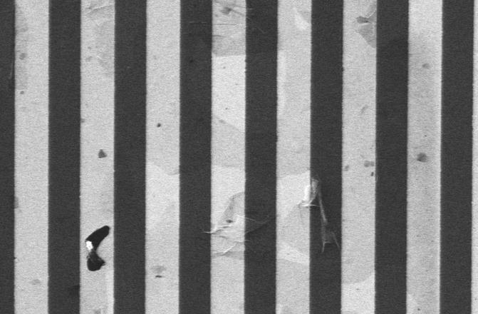
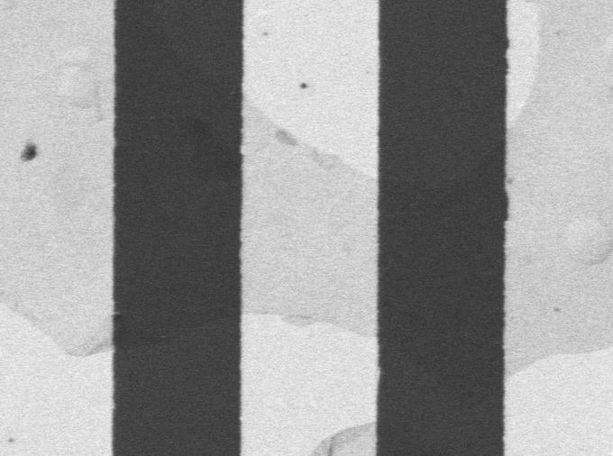
11 (a) (b) (c) (d) Fig. 2. Sahoo et al. 11
12 D band G band Intensity (arb. units) rgo GO Raman shift (cm -1 ) Fig. 3. Sahoo et al. 12
13 K 375 K 0.4 I (ma) V (Volt) Fig. 4. Sahoo et al. 13
14 R (Ohm) T (K) Fig. 5. Sahoo et al. 14
15 273 K 600 Sample K 500 OFF (Remove Ice) 450 Sample ON (Insert Ice) R (Ohm) 300 R (Ohm) 650 (a) Time (Sec) R(T) = *exp(-(t-68.78)/7.72) = sec Sample 1 =6 270 t1 = 0.58 sec R(T) = *exp(-(t-64.48)/6.35) Time (Sec) Fig. 6. Sahoo et al. 15 R (Ohm) sec 550 t2 R (Ohm) t2 Sample t1 = sec (b) 330
16 R (Ohm) R/R sample 1 = 12.1% R/R Sample 1 Pt 111 = 6.8% τ 2 = 6.35 sec τ r = sec 110 τ s = 0.58 sec τ s = 8.66 sec Pt Time (Sec) R (Ohm) Fig. 7. Sahoo et al. 16
Solvothermal Reduction of Chemically Exfoliated Graphene Sheets
 Solvothermal Reduction of Chemically Exfoliated Graphene Sheets Hailiang Wang, Joshua Tucker Robinson, Xiaolin Li, and Hongjie Dai* Department of Chemistry and Laboratory for Advanced Materials, Stanford
Conference Return Seminar- NANO2014,Moscow State University,Moscow,Russia Date: th July 2014
 Conference Return Seminar- NANO2014,Moscow State University,Moscow,Russia Date:13-1818 th July 2014 An electrochemical method for the synthesis of single and few layers graphene sheets for high temperature
Synthesis & Structural Study on Graphene Nano Particles
 Synthesis & Structural Study on Graphene Nano Particles L. Kashinath R. Senthil Kumar Y. Hayakawa Shizuko University Japan. G. Ravi Abstract: Graphene is one atom thick planar sheet of carbon atoms densely
Raman Imaging and Electronic Properties of Graphene
 Raman Imaging and Electronic Properties of Graphene F. Molitor, D. Graf, C. Stampfer, T. Ihn, and K. Ensslin Laboratory for Solid State Physics, ETH Zurich, 8093 Zurich, Switzerland ensslin@phys.ethz.ch
Intrinsic Electronic Transport Properties of High. Information
 Intrinsic Electronic Transport Properties of High Quality and MoS 2 : Supporting Information Britton W. H. Baugher, Hugh O. H. Churchill, Yafang Yang, and Pablo Jarillo-Herrero Department of Physics, Massachusetts
Molecular Dynamics Study of Thermal Rectification in Graphene Nanoribbons
 Int J Thermophys (2012) 33:986 991 DOI 10.1007/s10765-012-1216-y Molecular Dynamics Study of Thermal Rectification in Graphene Nanoribbons Jiuning Hu Xiulin Ruan Yong P. Chen Received: 26 June 2009 / Accepted:
Molecular Dynamics Study of Thermal Rectification in Graphene Nanoribbons
 Molecular Dynamics Study of Thermal Rectification in Graphene Nanoribbons Jiuning Hu 1* Xiulin Ruan 2 Yong P. Chen 3# 1School of Electrical and Computer Engineering and Birck Nanotechnology Center, Purdue
Characterization of partially reduced graphene oxide as room
 Supporting Information Characterization of partially reduced graphene oxide as room temperature sensor for H 2 Le-Sheng Zhang a, Wei D. Wang b, Xian-Qing Liang c, Wang-Sheng Chu d, Wei-Guo Song a *, Wei
The study on physical and mechanical properties of latex/graphene oxide composite film
 Journal of Physics: Conference Series PAPER OPEN ACCESS The study on physical and mechanical properties of latex/graphene oxide composite film To cite this article: S Gea et al 2018 J. Phys.: Conf. Ser.
SUPPORTING INFORMATION
 Electronic Supplementary Material (ESI) for Nanoscale. This journal is The Royal Society of Chemistry 2014 SUPPORTING INFORMATION Materials Graphite powder (SP-1 graphite) was obtained from Bay carbon.
Graphene. Tianyu Ye November 30th, 2011
 Graphene Tianyu Ye November 30th, 2011 Outline What is graphene? How to make graphene? (Exfoliation, Epitaxial, CVD) Is it graphene? (Identification methods) Transport properties; Other properties; Applications;
Iodide-mediated room temperature reduction of graphene oxide: a rapid chemical route for the synthesis of a bifunctional electrocatalyst
 Supporting Information Iodide-mediated room temperature reduction of graphene oxide: a rapid chemical route for the synthesis of a bifunctional electrocatalyst Ashok Kumar Das, 1 Manish Srivastav, 1 Rama
Supporting Information Available:
 Supporting Information Available: Photoresponsive and Gas Sensing Field-Effect Transistors based on Multilayer WS 2 Nanoflakes Nengjie Huo 1, Shengxue Yang 1, Zhongming Wei 2, Shu-Shen Li 1, Jian-Bai Xia
Influence of temperature and voltage on electrochemical reduction of graphene oxide
 Bull. Mater. Sci., Vol. 37, No. 3, May 2014, pp. 629 634. Indian Academy of Sciences. Influence of temperature and voltage on electrochemical reduction of graphene oxide XIUQIANG LI, DONG ZHANG*, PEIYING
Lithography-free Fabrication of High Quality Substrate-supported and. Freestanding Graphene devices
 Lithography-free Fabrication of High Quality Substrate-supported and Freestanding Graphene devices W. Bao 1, G. Liu 1, Z. Zhao 1, H. Zhang 1, D. Yan 2, A. Deshpande 3, B.J. LeRoy 3 and C.N. Lau 1, * 1
Vertical Alignment of Reduced Graphene Oxide/Fe-oxide Hybrids Using the Magneto-Evaporation Method
 Electronic Supplementary Information (ESI) Vertical Alignment of Reduced Graphene Oxide/Fe-oxide Hybrids Using the Magneto-Evaporation Method Sang Cheon Youn, Dae Woo Kim, Seung Bo Yang, Hye Mi Cho, Jae
A. Optimizing the growth conditions of large-scale graphene films
 1 A. Optimizing the growth conditions of large-scale graphene films Figure S1. Optical microscope images of graphene films transferred on 300 nm SiO 2 /Si substrates. a, Images of the graphene films grown
REDUCED GRAPHITE OXIDE-INDIUM TIN OXIDE COMPOSITES FOR TRANSPARENT ELECTRODE USING SOLUTION PROCESS
 18 TH INTERNATIONAL CONFERENCE ON COMPOSITE MATERIALS REDUCED GRAPHITE OXIDE-INDIUM TIN OXIDE COMPOSITES FOR TRANSPARENT ELECTRODE USING SOLUTION PROCESS K. S. Choi, Y. Park, K-.C. Kwon, J. Kim, C. K.
Chemical functionalization of graphene sheets by solvothermal reduction of suspension of
 Supplementary material Chemical functionalization of graphene sheets by solvothermal reduction of suspension of graphene oxide in N-methyl-2-pyrrolidone Viet Hung Pham, Tran Viet Cuong, Seung Hyun Hur,
GRAPHENE EFFECT ON EFFICIENCY OF TiO 2 -BASED DYE SENSITIZED SOLAR CELLS (DSSC)
") Communications in Physics, Vol. 26, No. 1 (2016), pp. 43-49 DOI:10.15625/0868-3166/26/1/7961 GRAPHENE EFFECT ON EFFICIENCY OF TiO 2 -BASED DYE SENSITIZED SOLAR CELLS (DSSC) NGUYEN THAI HA, PHAM DUY LONG,
Communications in Physics, Vol. 26, No. 1 (2016), pp. 43-49 DOI:10.15625/0868-3166/26/1/7961 GRAPHENE EFFECT ON EFFICIENCY OF TiO 2 -BASED DYE SENSITIZED SOLAR CELLS (DSSC) NGUYEN THAI HA, PHAM DUY LONG,
Hydrogenated CoO x Ni(OH) 2 nanosheet core shell nanostructures for high-performance asymmetric supercapacitors
 2 nanosheet core shell nanostructures for high-performance asymmetric supercapacitors") . Electronic Supplementary Material (ESI) for Nanoscale Electronic Supplementary Information (ESI) Hydrogenated CoO x nanowire @ Ni(OH) 2 nanosheet core shell nanostructures for high-performance asymmetric
. Electronic Supplementary Material (ESI) for Nanoscale Electronic Supplementary Information (ESI) Hydrogenated CoO x nanowire @ Ni(OH) 2 nanosheet core shell nanostructures for high-performance asymmetric
Efficient Preparation of Large-Area Graphene Oxide Sheets for Transparent Conductive Films
 Supporting Information Efficient Preparation of Large-Area Graphene Oxide Sheets for Transparent Conductive Films Jinping Zhao, Songfeng Pei, Wencai Ren*, Libo Gao and Hui-Ming Cheng* Shenyang National
sheets in the exfoliation step
 Optimization of the size and yield of graphene oxide sheets in the exfoliation step Cristina Botas, Ana M. Pérez-Mas, Patricia Álvarez, Ricardo Santamaría, Marcos Granda, Clara Blanco, and Rosa Menéndez
Ambipolar bistable switching effect of graphene
 Ambipolar bistable switching effect of graphene Young Jun Shin, 1,2 Jae Hyun Kwon, 1,2 Gopinadhan Kalon, 1,2 Kai-Tak Lam, 1 Charanjit S. Bhatia, 1 Gengchiau Liang, 1 and Hyunsoo Yang 1,2,a) 1 Department
Supporting Information. High-Performance Strain Sensors with Fish Scale-Like Graphene. Sensing Layers for Full-Range Detection of Human Motions
 Supporting Information High-Performance Strain Sensors with Fish Scale-Like Graphene Sensing Layers for Full-Range Detection of Human Motions Qiang Liu, Ji Chen, Yingru Li, and Gaoquan Shi* Department
TRANSVERSE SPIN TRANSPORT IN GRAPHENE
 International Journal of Modern Physics B Vol. 23, Nos. 12 & 13 (2009) 2641 2646 World Scientific Publishing Company TRANSVERSE SPIN TRANSPORT IN GRAPHENE TARIQ M. G. MOHIUDDIN, A. A. ZHUKOV, D. C. ELIAS,
Overview. Carbon in all its forms. Background & Discovery Fabrication. Important properties. Summary & References. Overview of current research
 Graphene Prepared for Solid State Physics II Pr Dagotto Spring 2009 Laurene Tetard 03/23/09 Overview Carbon in all its forms Background & Discovery Fabrication Important properties Overview of current
High Performance, Low Operating Voltage n-type Organic Field Effect Transistor Based on Inorganic-Organic Bilayer Dielectric System
 Journal of Physics: Conference Series PAPER OPEN ACCESS High Performance, Low Operating Voltage n-type Organic Field Effect Transistor Based on Inorganic-Organic Bilayer Dielectric System To cite this
Lithography-Free Fabrication of High Quality Substrate- Supported and Freestanding Graphene Devices
 98 DOI 10.1007/s12274-010-1013-5 Research Article Lithography-Free Fabrication of High Quality Substrate- Supported and Freestanding Graphene Devices Wenzhong Bao 1, Gang Liu 1, Zeng Zhao 1, Hang Zhang
Radiation Induced Reduction: A Effect and Clean Route to
 Supporting Information for Radiation Induced Reduction: A Effect and Clean Route to Synthesize Functionalized Graphene Bowu ZHANG, a, b Linfan LI, a Ziqiang WANG, a Siyuan XIE, a, b Yujie ZHANG, c Yue
High Quality Thin Graphene Films from Fast. Research Center for Applied Sciences, Academia Sinica, Taipei, 11529, Taiwan
 Supporting Materials High Quality Thin Graphene Films from Fast Electrochemical Exfoliation Ching-Yuan Su, Ang-Yu Lu #, Yanping Xu, Fu-Rong Chen #, Andrei N. Khlobystov $ and Lain-Jong Li * Research Center
Supplementary Information
 Supplementary Information Plasma-assisted reduction of graphene oxide at low temperature and atmospheric pressure for flexible conductor applications Seung Whan Lee 1, Cecilia Mattevi 2, Manish Chhowalla
Initial Stages of Growth of Organic Semiconductors on Graphene
 Initial Stages of Growth of Organic Semiconductors on Graphene Presented by: Manisha Chhikara Supervisor: Prof. Dr. Gvido Bratina University of Nova Gorica Outline Introduction to Graphene Fabrication
AN IMPROVED METHOD FOR TRANSFERRING GRAPHENE GROWN BY CHEMICAL VAPOR DEPOSITION
 NANO: Brief Reports and Reviews Vol. 7, No. 1 (2012) 1150001 (6 pages) World Scienti c Publishing Company DOI: 10.1142/S1793292011500019 AN IMPROVED METHOD FOR TRANSFERRING GRAPHENE GROWN BY CHEMICAL VAPOR
Tunneling characteristics of graphene
 Tunneling characteristics of graphene Young Jun Shin, 1,2 Gopinadhan Kalon, 1,2 Jaesung Son, 1 Jae Hyun Kwon, 1,2 Jing Niu, 1 Charanjit S. Bhatia, 1 Gengchiau Liang, 1 and Hyunsoo Yang 1,2,a) 1 Department
SUPPLEMENTARY INFORMATION
 SUPPLEMENTARY INFORMATION Facile Synthesis of High Quality Graphene Nanoribbons Liying Jiao, Xinran Wang, Georgi Diankov, Hailiang Wang & Hongjie Dai* Supplementary Information 1. Photograph of graphene
Spin Injection into a Graphene Thin Film at Room Temperature
 Spin Injection into a Graphene Thin Film at Room Temperature Megumi Ohishi, Masashi Shiraishi*, Ryo Nouchi, Takayuki Nozaki, Teruya Shinjo, and Yoshishige Suzuki Graduate School of Engineering Science,
Effects of interaction of electron-donor and accepter molecules on the electronic structure of graphene
 Effects of interaction of electron-donor and accepter molecules on the electronic structure of graphene Rakesh Voggu 1, Barun Das 1, 2, Chandra Sekhar Rout, 1 1, 2,* and C. N. R. Rao 1 Chemistry and Physics
Three-dimensional Multi-recognition Flexible Wearable
 Electronic Supplementary Material (ESI) for ChemComm. This journal is The Royal Society of Chemistry 2016 This journal is The Royal Society of Chemistry 2016 Supporting Information Three-dimensional Multi-recognition
Supporting Information
 Supporting Information Oxygen Reduction on Graphene-Carbon Nanotube Composites Doped Sequentially with Nitrogen and Sulfur Drew C. Higgins, Md Ariful Hoque, Fathy Hassan, Ja-Yeon Choi, Baejung Kim, Zhongwei
Graphene Chemical Vapor Deposition (CVD) Growth
 Growth") ECE440 Nanoelectronics Graphene Chemical Vapor Deposition (CVD) Growth Zheng Yang Timeline of graphene CVD growth Exfoliation
ECE440 Nanoelectronics Graphene Chemical Vapor Deposition (CVD) Growth Zheng Yang Timeline of graphene CVD growth Exfoliation
Electronic Supplementary Information
 Electronic Supplementary Information Dual N-type Doped Reduced Graphene Oxide Field Effect Transistors Controlled by Semiconductor Nanocrystals Luyang Wang, Jie Lian, Peng Cui, Yang Xu, Sohyeon Seo, Junghyun
Supporting information
 Supporting information Influence of electrolyte composition on liquid-gated carbon-nanotube and graphene transistors By: Iddo Heller, Sohail Chatoor, Jaan Männik, Marcel A. G. Zevenbergen, Cees Dekker,
GRAPHENE ON THE Si-FACE OF SILICON CARBIDE USER MANUAL
 GRAPHENE ON THE Si-FACE OF SILICON CARBIDE USER MANUAL 1. INTRODUCTION Silicon Carbide (SiC) is a wide band gap semiconductor that exists in different polytypes. The substrate used for the fabrication
Graphene Novel Material for Nanoelectronics
 Graphene Novel Material for Nanoelectronics Shintaro Sato Naoki Harada Daiyu Kondo Mari Ohfuchi (Manuscript received May 12, 2009) Graphene is a flat monolayer of carbon atoms with a two-dimensional honeycomb
Surface Modifications of Graphene-based Polymer Nanocomposites by Different Synthesis Techniques
 Surface Modifications of Graphene-based Polymer Nanocomposites by Different Synthesis Techniques Journal: 2012 MRS Spring Meeting Manuscript ID: MRSS12-1451-DD14-02.R1 Manuscript Type: Symposium DD Date
The study of wettability in reduced graphene oxide film on copper substrate using electrostatic spray deposition technique
 Journal of Physics: Conference Series PAPER OPEN ACCESS The study of wettability in reduced graphene oxide film on copper substrate using electrostatic spray deposition technique To cite this article:
Effect of the Substrate on Phonon Properties of Graphene. Estimated by Raman Spectroscopy
 This is a pre-print of an article published in Journal of Low Temperature Physics. The final authenticated version is available online at: https://doi.org/10.1007/s10909-017807-x Effect of the Substrate
Solution-processable graphene nanomeshes with controlled
 Supporting online materials for Solution-processable graphene nanomeshes with controlled pore structures Xiluan Wang, 1 Liying Jiao, 1 Kaixuan Sheng, 1 Chun Li, 1 Liming Dai 2, * & Gaoquan Shi 1, * 1 Department
Supplementary Figure S1. AFM images of GraNRs grown with standard growth process. Each of these pictures show GraNRs prepared independently,
 Supplementary Figure S1. AFM images of GraNRs grown with standard growth process. Each of these pictures show GraNRs prepared independently, suggesting that the results is reproducible. Supplementary Figure
IMPROVEMENT IN MECHANICAL PROPERTIES OF MODIFIED GRAPHENE/EPOXY NANOCOMPOSITES
 18 TH INTERNATIONAL CONFERENCE ON COMPOSITE MATERIALS IMPROVEMENT IN MECHANICAL PROPERTIES OF MODIFIED 1 Introduction Since first successfully separated from graphite by micromechanical cleavage [1], graphene
Transparent Electrode Applications
 Transparent Electrode Applications LCD Solar Cells Touch Screen Indium Tin Oxide (ITO) Zinc Oxide (ZnO) - High conductivity - High transparency - Resistant to environmental effects - Rare material (Indium)
Transient Photocurrent Measurements of Graphene Related Materials
 Transient Photocurrent Measurements of Graphene Related Materials P. Srinivasa Rao Mentor: Prof. dr. Gvido Bratina Laboratory of Organic Matter Physics University of Nova Gorica 1 Contents: 1. Electrical
Resistive switching behavior of reduced graphene oxide memory cells for low power nonvolatile device application
 Resistive switching behavior of reduced graphene oxide memory cells for low power nonvolatile device application S. K. Pradhan, Bo, Xiao, S. Mishra, A. Killam, A. K. Pradhan Center for Materials Research,
Supporting Information
 Electronic Supplementary Material (ESI) for Nanoscale. This journal is The Royal Society of Chemistry 2016 Supporting Information Graphene transfer method 1 : Monolayer graphene was pre-deposited on both
Wafer-scale fabrication of graphene
 Wafer-scale fabrication of graphene Sten Vollebregt, MSc Delft University of Technology, Delft Institute of Mircosystems and Nanotechnology Delft University of Technology Challenge the future Delft University
Electrochemically Exfoliated Graphene as Solution-Processable, Highly-Conductive Electrodes for Organic Electronics
 Supporting Information Electrochemically Exfoliated Graphene as Solution-Processable, Highly-Conductive Electrodes for Organic Electronics Khaled Parvez, Rongjin Li, Sreenivasa Reddy Puniredd, Yenny Hernandez,
Supporting Information
 Supporting Information Repeated Growth Etching Regrowth for Large-Area Defect-Free Single-Crystal Graphene by Chemical Vapor Deposition Teng Ma, 1 Wencai Ren, 1 * Zhibo Liu, 1 Le Huang, 2 Lai-Peng Ma,
A project report on SYNTHESIS AND CHARACTERISATION OF COPPER NANOPARTICLE-GRAPHENE COMPOSITE. Submitted by Arun Kumar Yelshetty Roll no 410 CY 5066
 A project report on SYNTHESIS AND CHARACTERISATION OF COPPER NANOPARTICLE-GRAPHENE COMPOSITE Submitted by Arun Kumar Yelshetty Roll no 410 CY 5066 Under the guidance of Prof. (Ms). Sasmita Mohapatra Department
Synthesis and Characterization of Graphene by Raman Spectroscopy
 Journal of Materials Sciences and Applications 2015; 1(3): 130-135 Published online June 20, 2015 (http://www.aascit.org/journal/jmsa) Synthesis and Characterization of Graphene by Raman Spectroscopy Hilal
Raman spectroscopy at the edges of multilayer graphene
 Raman spectroscopy at the edges of multilayer graphene Q. -Q. Li, X. Zhang, W. -P. Han, Y. Lu, W. Shi, J. -B. Wu, P. -H. Tan* State Key Laboratory of Superlattices and Microstructures, Institute of Semiconductors,
Supporting Information. by Hexagonal Boron Nitride
 Supporting Information High Velocity Saturation in Graphene Encapsulated by Hexagonal Boron Nitride Megan A. Yamoah 1,2,, Wenmin Yang 1,3, Eric Pop 4,5,6, David Goldhaber-Gordon 1 * 1 Department of Physics,
Graphene The Search For Two Dimensions. Christopher Scott Friedline Arizona State University
 Graphene The Search For Two Dimensions Christopher Scott Friedline Arizona State University What Is Graphene? Single atomic layer of graphite arranged in a honeycomb crystal lattice Consists of sp 2 -bonded
Supplementary Material for. Zinc Oxide-Black Phosphorus Composites for Ultrasensitive Nitrogen
 Electronic Supplementary Material (ESI) for Nanoscale Horizons. This journal is The Royal Society of Chemistry 2018 Supplementary Material for Zinc Oxide-Black Phosphorus Composites for Ultrasensitive
Multicolor Graphene Nanoribbon/Semiconductor Nanowire. Heterojunction Light-Emitting Diodes
 Multicolor Graphene Nanoribbon/Semiconductor Nanowire Heterojunction Light-Emitting Diodes Yu Ye, a Lin Gan, b Lun Dai, *a Hu Meng, a Feng Wei, a Yu Dai, a Zujin Shi, b Bin Yu, a Xuefeng Guo, b and Guogang
Graphene FETs with Combined Structure and Transparent Top
 Available online at www.sciencedirect.com Physics Procedia 32 (2012 ) 869 874 18th International Vacuum Congress (IVC-18) Graphene FETs with Combined Structure and Transparent Top Yuanlin Yuan a, Zhen
Supplementary Figure 1 A schematic representation of the different reaction mechanisms
 Supplementary Figure 1 A schematic representation of the different reaction mechanisms observed in electrode materials for lithium batteries. Black circles: voids in the crystal structure, blue circles:
performance electrocatalytic or electrochemical devices. Nanocrystals grown on graphene could have
 Nanocrystal Growth on Graphene with Various Degrees of Oxidation Hailiang Wang, Joshua Tucker Robinson, Georgi Diankov, and Hongjie Dai * Department of Chemistry and Laboratory for Advanced Materials,
Preparation of graphene relying on porphyrin exfoliation of graphite
 Electronic Supplementary Information (ESI) for: Preparation of graphene relying on porphyrin exfoliation of graphite Jianxin Geng, Byung-Seon Kong, Seung Bo Yang and Hee-Tae Jung* National Research Laboratory,
Supporting Information
 Electronic Supplementary Material (ESI) for RSC Advances. This journal is The Royal Society of Chemistry 2014 Supporting Information Au nanoparticles supported on magnetically separable Fe 2 O 3 - graphene
Sub-5 nm Patterning and Applications by Nanoimprint Lithography and Helium Ion Beam Lithography
 Sub-5 nm Patterning and Applications by Nanoimprint Lithography and Helium Ion Beam Lithography Yuanrui Li 1, Ahmed Abbas 1, Yuhan Yao 1, Yifei Wang 1, Wen-Di Li 2, Chongwu Zhou 1 and Wei Wu 1* 1 Department
Intrinsic structure and friction properties of graphene and graphene oxide nanosheets studied by scanning probe microscopy
 Bull. Mater. Sci., Vol. 36, No. 6, November 2013, pp. 1073 1077. c Indian Academy of Sciences. Intrinsic structure and friction properties of graphene and graphene oxide nanosheets studied by scanning
We are IntechOpen, the world s leading publisher of Open Access books Built by scientists, for scientists. International authors and editors
 We are IntechOpen, the world s leading publisher of Open Access books Built by scientists, for scientists 4,100 116,000 120M Open access books available International authors and editors Downloads Our
CVD growth of Graphene. SPE ACCE presentation Carter Kittrell James M. Tour group September 9 to 11, 2014
 CVD growth of Graphene SPE ACCE presentation Carter Kittrell James M. Tour group September 9 to 11, 2014 Graphene zigzag armchair History 1500: Pencil-Is it made of lead? 1789: Graphite 1987: The first
Supporting Information
 Supporting Information Wiley-VCH 2013 69451 Weinheim, Germany 3D Honeycomb-Like Structured Graphene and Its High Efficiency as a Counter-Electrode Catalyst for Dye-Sensitized Solar Cells** Hui Wang, Kai
Enhanced photocurrent of ZnO nanorods array sensitized with graphene. quantum dots
 Electronic Supplementary Material (ESI) for RSC Advances. This journal is The Royal Society of Chemistry 2015 Enhanced photocurrent of ZnO nanorods array sensitized with graphene quantum dots Bingjun Yang,
Functionalization of Graphene Oxide by Two-Step Alkylation
 Full Paper Macromolecular Functionalization of Graphene Oxide by Two-Step Alkylation Yi Huang, Weibo Yan, Yanfei Xu, Lu Huang, Yongsheng Chen * A new reaction sequence for the chemical functionalization
Fabrication of graphene nanogap with crystallographically matching edges and its. electron emission properties
 Fabrication of graphene nanogap with crystallographically matching edges and its electron emission properties H. M. Wang, 1 Z. Zheng, 1 Y.Y.Wang, 1 J.J. Qiu, Z.B. Guo, Z. X. Shen, 1 and T. Yu 1,* 1 Division
Electronic Supplementary Information. Microwave-assisted, environmentally friendly, one-pot preparation. in electrocatalytic oxidation of methanol
 Electronic Supplementary Information Microwave-assisted, environmentally friendly, one-pot preparation of Pd nanoparticles/graphene nanocomposites and their application in electrocatalytic oxidation of
Hybrid Surface-Phonon-Plasmon Polariton Modes in Graphene /
 Supplementary Information: Hybrid Surface-Phonon-Plasmon Polariton Modes in Graphene / Monolayer h-bn stacks Victor W. Brar 1,2, Min Seok Jang 3,, Michelle Sherrott 1, Seyoon Kim 1, Josue J. Lopez 1, Laura
Raman spectroscopy of graphene on different substrates and influence of defects
 Bull. Mater. Sci., Vol. 31, No. 3, June 2008, pp. 579 584. Indian Academy of Sciences. Raman spectroscopy of graphene on different substrates and influence of defects ANINDYA DAS, BISWANATH CHAKRABORTY
Seminars in Nanosystems - I
 Seminars in Nanosystems - I Winter Semester 2011/2012 Dr. Emanuela Margapoti Emanuela.Margapoti@wsi.tum.de Dr. Gregor Koblmüller Gregor.Koblmueller@wsi.tum.de Seminar Room at ZNN 1 floor Topics of the
PARALLEL MEASUREMENT OF CONDUCTIVE AND CONVECTIVE THERMAL TRANSPORT OF MICRO/NANOWIRES BASED ON RAMAN MAPPING
 Proceedings of the Asian Conference on Thermal Sciences 217, 1st ACTS March 26-3, 217, Jeju Island, Korea ACTS-4 PARALLEL MEASUREMENT OF CONDUCTIVE AND CONVECTIVE THERMAL TRANSPORT OF MICRO/NANOWIRES BASED
MICROWAVE AND MILLIMETERWAVE ELECTRICAL PERMITTIVITY OF GRAPHENE MONOLAYER. G. Konstantinidis 3
 1 MICROWAVE AND MILLIMETERWAVE ELECTRICAL PERMITTIVITY OF GRAPHENE MONOLAYER Alina Cismaru 1, Mircea Dragoman 1*, Adrian Dinescu 1, Daniela Dragoman 2, G. Stavrinidis, G. Konstantinidis 3 1 National Institute
One-step reduction, characterization and magnetic behaviour of exfoliated graphene oxide
 Materials Science-Poland, 31(1), 2013, pp. 59-64 http://www.materialsscience.pwr.wroc.pl/ DOI: 10.2478/s13536-012-0068-2 One-step reduction, characterization and magnetic behaviour of exfoliated graphene
Supplementary Figure 1 Dark-field optical images of as prepared PMMA-assisted transferred CVD graphene films on silicon substrates (a) and the one
 and the one") Supplementary Figure 1 Dark-field optical images of as prepared PMMA-assisted transferred CVD graphene films on silicon substrates (a) and the one after PBASE monolayer growth (b). 1 Supplementary Figure
Supplementary Figure 1 Dark-field optical images of as prepared PMMA-assisted transferred CVD graphene films on silicon substrates (a) and the one after PBASE monolayer growth (b). 1 Supplementary Figure
Nanostrukturphysik (Nanostructure Physics)
") Nanostrukturphysik (Nanostructure Physics) Prof. Yong Lei & Dr. Yang Xu Fachgebiet 3D-Nanostrukturierung, Institut für Physik Contact: yong.lei@tu-ilmenau.de; yang.xu@tu-ilmenau.de Office: Unterpoerlitzer
Nanostrukturphysik (Nanostructure Physics) Prof. Yong Lei & Dr. Yang Xu Fachgebiet 3D-Nanostrukturierung, Institut für Physik Contact: yong.lei@tu-ilmenau.de; yang.xu@tu-ilmenau.de Office: Unterpoerlitzer
Synthesis of a highly conductive and large surface area graphene oxide hydrogel and its use in a supercapacitor
 Electronic Supplementary Information for: Synthesis of a highly conductive and large surface area graphene oxide hydrogel and its use in a supercapacitor Van Hoang Luan, a Huynh Ngoc Tien, a Le Thuy Hoa,
ELECTROMAGNETIC PROPERTIES OF COBALT REDUCED GRAPHENE OXIDE (CO-RGO)/ EPOXY COMPOSITES
/ EPOXY COMPOSITES") THE 19 TH INTERNATIONAL CONFERENCE ON COMPOSITE MATERIALS ELECTROMAGNETIC PROPERTIES OF COBALT REDUCED GRAPHENE OXIDE (CO-RGO)/ EPOXY COMPOSITES Y. Wang 1, Y. Zhao 1 *, Y. Su 1, X. Lu 2 1 School of Materials
THE 19 TH INTERNATIONAL CONFERENCE ON COMPOSITE MATERIALS ELECTROMAGNETIC PROPERTIES OF COBALT REDUCED GRAPHENE OXIDE (CO-RGO)/ EPOXY COMPOSITES Y. Wang 1, Y. Zhao 1 *, Y. Su 1, X. Lu 2 1 School of Materials
Graphene is a single, two-dimensional nanosheet of aromatic sp 2 hybridized carbons that
 Chemical Identity and Applications of Graphene-Titanium Dioxide Graphene is a single, two-dimensional nanosheet of aromatic sp 2 hybridized carbons that enhances the performance of photocatalysts. 1 The
Optimizing Graphene Morphology on SiC(0001)
") Optimizing Graphene Morphology on SiC(0001) James B. Hannon Rudolf M. Tromp Graphene sheets Graphene sheets can be formed into 0D,1D, 2D, and 3D structures Chemically inert Intrinsically high carrier mobility
Optimizing Graphene Morphology on SiC(0001) James B. Hannon Rudolf M. Tromp Graphene sheets Graphene sheets can be formed into 0D,1D, 2D, and 3D structures Chemically inert Intrinsically high carrier mobility
Supporting Information
 Electronic Supplementary Material (ESI) for Journal of Materials Chemistry A. This journal is The Royal Society of Chemistry 2015 Supporting Information 1. Synthesis of perovskite materials CH 3 NH 3 I
The GO was synthesized by oxidation of purified natural small graphite and graphite
 Jing-He Yang, a,b Geng Sun, a Yongjun Gao, a Huabo Zhao, a Pei Tang, a Juan Tan, b Lu b and Ding Ma*,a An-Hui a Beijing National Laboratory for Molecular Sciences, College of Chemistry and Molecular Engineering,
Synthesis and Characterization of Exfoliated Graphite (EG) and to Use it as a Reinforcement in Zn-based Metal Matrix Composites
 and to Use it as a Reinforcement in Zn-based Metal Matrix Composites") Synthesis and Characterization of Exfoliated Graphite (EG) and to Use it as a Reinforcement in Zn-based Metal Matrix Composites Here H 2 SO 4 was used as an intercalant and H 2 O 2 as an oxidant. Expandable
Synthesis and Characterization of Exfoliated Graphite (EG) and to Use it as a Reinforcement in Zn-based Metal Matrix Composites Here H 2 SO 4 was used as an intercalant and H 2 O 2 as an oxidant. Expandable
Graphene A One-Atom-Thick Material for Microwave Devices
 ROMANIAN JOURNAL OF INFORMATION SCIENCE AND TECHNOLOGY Volume 11, Number 1, 2008, 29 35 Graphene A One-Atom-Thick Material for Microwave Devices D. DRAGOMAN 1, M. DRAGOMAN 2, A. A. MÜLLER3 1 University
Supporting Information. Temperature dependence on charge transport behavior of threedimensional
 Supporting Information Temperature dependence on charge transport behavior of threedimensional superlattice crystals A. Sreekumaran Nair and K. Kimura* University of Hyogo, Graduate School of Material
Simultaneous Nitrogen Doping and Reduction of Graphene Oxide
 Published on Web 10/09/2009 Simultaneous Nitrogen Doping and Reduction of Graphene Oxide Xiaolin Li, Hailiang Wang, Joshua T. Robinson, Hernan Sanchez, Georgi Diankov, and Hongjie Dai* Department of Chemistry,
Controlling Graphene Ultrafast Hot Carrier Response from Metal-like. to Semiconductor-like by Electrostatic Gating
 Controlling Graphene Ultrafast Hot Carrier Response from Metal-like to Semiconductor-like by Electrostatic Gating S.-F. Shi, 1,2* T.-T. Tang, 1 B. Zeng, 1 L. Ju, 1 Q. Zhou, 1 A. Zettl, 1,2,3 F. Wang 1,2,3
Supplementary Information for. Origin of New Broad Raman D and G Peaks in Annealed Graphene
 Supplementary Information for Origin of New Broad Raman D and G Peaks in Annealed Graphene Jinpyo Hong, Min Kyu Park, Eun Jung Lee, DaeEung Lee, Dong Seok Hwang and Sunmin Ryu* Department of Applied Chemistry,
Supplementary material for High responsivity mid-infrared graphene detectors with antenna-enhanced photo-carrier generation and collection
 Supplementary material for High responsivity mid-infrared graphene detectors with antenna-enhanced photo-carrier generation and collection Yu Yao 1, Raji Shankar 1, Patrick Rauter 1, Yi Song 2, Jing Kong