Two-Dimensional Honeycomb Monolayer of Nitrogen Group. Elements and the Related Nano-Structure: A First-Principle Study
|
|
|
- Meredith Washington
- 6 years ago
- Views:
Transcription
1 Two-Dimensional Honeycomb Monolayer of Nitrogen Group Elements and the Related Nano-Structure: A First-Principle Study Jason Lee, Wen-Chuan Tian,Wei-Liang Wang, Dao-Xin Yao * State Key Laboratory of Optoelectronic Materials and Technologies, School of Physics and Engineering, Sun Yat-Sen University, Guangzhou , China Corresponding author: yaodaox@mail.sysu.edu.cn Abstract In recent years, two-dimensional material attracts great attention, and new twodimensional materials are being predicted, discovered and studied. Based on the idea of octet stability, we predict a new family of two-dimensional material: honeycomb monolayer of nitrogen group elements in the periodic table. From our calculation we prove the existence of two-dimensional structure of all these elements, and their electronic structure has been intensively studied. The effect of spin-orbit coupling on the band structure has also been investigated. Based on analysis of projected density of states, we argue that only the s and p orbitals are sufficient to describe the electronic structure, and a tight-binding model with spin-orbit coupling using only s and p orbitals is constructed, and the parameters are obtained by fitting the band structures. We also shed light on the electronic structure of zigzag nano-ribbon and armchair nano-ribbon, and found spin-polarized ferromagnetic edge states. We look forward to the synthesis and applications of these materials. Key Words: nitrogen group element, honeycomb, two-dimensional, nano-ribbon I. Introduction Various Two-dimensional materials are booming in recent years 1, 2. Successful exfoliation of graphene marked the beginning of study of two-dimensional materials 3,4,5. Particularly, black phosphorus has begun to be synthesized and studied 6,7,8. It was argued that black phosphorus has high carrier mobility, and has certain advantage over other two-dimensional materials 8. Recently, another allotrope of phosphorus call blue phosphorus has been predicted, and it has much larger band gap than black phosphorus 9. In addition to phosphorus, two-dimensional nitrogen atomic sheet has been grown epitaxially on GaAs(001) surface 10. Phosphorus and nitrogen belong to the nitrogen group (VA) elements in the periodic table. They have five valence electrons, and needs three additional electrons to achieve octet stability. In other words, if these elements form a two-dimensional honeycomb lattice so that each atom bonds to three neighboring sites, they achieve octet stability. Based on this idea, we argue that VA elements have stable form of two-dimensional honeycomb structure. In this work, we theoretically predict that VA elements in the periodic table, have two-dimensional stable structure. In fact, several studies investigate the properties of VA elements 11,12, but there is no systemic study yet.
2 In this paper, we use first-principle calculation to explore the unknown phase of VA elements in the periodic table. Our calculation is based on Plane Augmented Wave (PAW) with Perdew-Burke-Ernzerh (PBE) of exchange-correlation 13 as implemented in the Vienna Ab initio Simulation Package (VASP) code 14. To ensure reliable result, we use large energy cut-off of 400eV for bulk and monolayer, but we use default cutoff energy for nano-ribbon. The systems are restricted to periodic boundary conditions in the study of bulk properties, while in the study of system with lower dimension (monolayer and nano-ribbon), a vacuum at least 15 Å thick is inserted to eliminate the interaction between different units. For optimization, ions are relaxed using conjugategradient algorithm until the total force is no greater than 0.01eV/ Å. Grimme s scheme for van de Waals (vdw) correction 15 is used for optimization of bulk structure, and results are compared with those obtained without vdw correction. Unfortunately, vdw correction is not included in case of bismuth because of lack of parameters. Some vdw scheme with higher precision 16 could have been used, but getting accurate vdw energy is not the main interest of this paper, and a simple time-saving scheme of Grimme is sufficient to prove our statements. Spin-orbit Coupling (SOC) is included only in the calculation of band structure of monolayer. II. Layered Structure and Monolayers The three-dimensional AB stacking structures of VA elements are obtained from our calculation. Their structures are similar, as shown in Figure 1. The optimized threedimensional structures of nitrogen (N), phosphorus (P), arsenic (As), antimony (Sb) and Bismuth (Bi) are listed in table 1. It is clear that the inclusion of vdw interaction does not change the structure parameters within a layer dramatically, even though the interlayer distance d is decreased by about 1Å for P and As. The calculated lattice constant a and bond length l bond for blue phosphorus are 3.32Å/3.28 Å (with/without vdw) and 2.27 Å respectively for bulk, and 3.28 Å and 2.27 Å for monolayer, in agreement with previous study by Z. Zhu et.al. 7. But their inter-layer distance is larger than our result. We have also calculated vibration frequencies for monolayers of all VA elements, and no imaginary frequency is found, suggesting the stability of all these structures. It is necessary to point out that, during the optimization process of three-dimensional structure of N, we found the tiny jittering of totally energy as the inter-layer distance changes. This may suggest that interaction between N layers are extraordinarily weak (if they have any) and the computer finds it difficult to optimize the structure to minimize the total energy. It means that these layers can detach from each other very easily, therefore the three-dimensional structure of N may not exists, and it is just a possibility. There is no monotonous increase of inter-layer distance d, but we do see the monotonous increases of lattice constant a, buckling z, bond length l bond and the nearest distance between atoms in different layers l with respect to increasing atomic
3 number from P to Bi are clear. This is in agreement with the periodic law of elements. Interestingly, if we compare the bond length with twice the covalent radius, the bond length is a little bit longer. For all cases, the bond length l bond s are much smaller than the nearest distance between atoms in different layers l s. From table 1 we can see, the inclusion of vdw correction mainly affects the inter-layer distance d while having minor effect on the lattice constant a, buckling z and bond length l bond. When vdw is included, all the l s are about twice the vdw radii.all these phenomena suggest that layers couple with each other by weak vdw interaction and thus can easily exfoliated to form monolayer 17. All the monolayers have silicone-like structures, and resembles that of the bulk. The structure parameters of monolayer only slightly differ from that of the bulk, which indicates the weak inter-layer vdw interaction. Moreover, it is clear that the structure parameters for nitrogen is much smaller than any other VA elements. As in the case of bulk structure, the bond lengths are a little bit longer than twice the covalent radii. III. Electronic structure of monolayer Electronic structures obtained from our first-principle calculation are very similar, as shown in Figure 2 (without SOC) and Figure 3 (with SOC). Three branches of bands are evident, as shown in three different colors in Figure 2 and Figure 3. For nitrogen monolayer, the band structure is similar to that of silicene 18, with the lower branch and the middle branch entangled. As atomic number increases, the lower branch gradually disentangled from the middle one, becomes lower in energy, and forms a graphene-like band structure. Meanwhile, the ranges of all these three bands shrink, suggesting the weakening interaction between orbitals as the covalent bonds become longer. As the atomic number increases, the effect of SOC on band structure increases. SOC mainly affects the middle branch and the upper branch of bands, and has no noticeable influence on the lower branch. As we will see in the projected density of states (PDOS), this is because the lower branch is made up of s orbit and while the middle and upper branch are made up of p orbitals. However, the overall effect of SOC is still minute. The calculated band gaps are listed in table 2. We obtained a smaller band gap (1.97eV) than previous study of blue phosphorus monolayer (over 2eV) 9. The band gap decreases from 3.70eV of nitrogen to just 0.55eV/0.42eV(without/with SOC) of Bi, which means they change from insulator to semiconductor. This makes sense in that the metal character increases as atomic number increases in VA elements. Without SOC, all these band structures have indirect band gaps except Bi. When SOC is included in the calculation, all band structures have indirect band gaps. As the atomic number increases, both the valence band maximum (VBM) and the conducting band minimum (CBM) shift towards Γ point in the BZ. In case of Bi, when SOC is not included, both the VBM and CBM rest in Γ point, making it a direct band gap. But strangely enough, when SOC is included, the VBM of bismuth shifts away from Γ point again, making it an indirect
4 band gap. We also try applying strain to bismuth monolayer, and find that the band gap decreases with increasing strain, then it closes for approximately 5% strain, and it reopens if strain keep increasing. This is consistent with previous studies that focus on the topological aspect of bismuth monolayer 12. The calculated PDOS of VA element monolayers is presented in Figure 4. The evolution of orbital character of band structure can be seen from PDOS. For nitrogen monolayer, the lower branch mainly comes from 2s orbital while the upper one mainly from 2p orbitals, and in the middle branch, 2s and 2p orbital are highly mixed, making roughly the same contribution to this branch of bands. For phosphorus, the s component of the lower branch increases with decreasing p character, but the middle and upper branch takes a totally opposite trend, which is the p character increases as s character decreases. This trend persists all the way to bismuth. This can explain why SOC can influence the middle and upper branch of bands while having no noticeable effect on the lower branch: SOC have nonzero contribution to p orbitals, but it vanishes for s orbital because the angular moment of s orbital is zero. Moreover, from arsenic on, d character begins to creep up, but its contribution is still minute for all cases. Another interesting trend is that, the gap between the lower branch and the middle branch enlarges as atomic number increases, which is an indication of increasing relativistic effect. Based on the analysis of PDOS, it is clear that a tight-binding (TB) model with just s and p orbitals of both atoms is sufficient to describe the system. We could have included d orbitals to give a more accurate description, but it may not be necessary. Recently Zolymoi et. al. have constructed a TB model for silicane and germanane with just s and p orbital 19. In view of certain similarity between the systems we study and the system in Zolymoi s paper (silicane and germanane), we can construct a similar TB model, with minor modification. H = H 0 + H 1 + H 2 + H SO H 0 = [ε s a (R i )a(r i ) + ε p b (R i ) b(r i )] i H 1 = [h s (i, j) + h p (i, j) + h sp (i, j) + h. c. ] i,j H 2 = [h s (i, j) + h p (i, j) + h sp (i, j) + h. c. ] i,j H SO = iλ I ν ij σ z αβ b α (R i ) b β (R j ) i,j αβ + iλ R μ ij (e ij σ) z b α (R i ) b β (R j ) i,j αβ h s (i, j) = γ ss a (R i )a(r j )
5 h p (i, j) = γ ppσ [e ij b (R i )][e ij b(r j )] + γ ppπ {b (R i ) b(r j ) [e ij b (R i )][e ij b(r j )]} h sp (i, j) = γ sp a (R i ) (e ij b(r j )) h s (i, j) = γ ss a (R i )a(r j ) h p (i, j) = γ ppσ [e ij b (R i )][e ij b(r j )] + γ ppπ {b (R i ) b(r j ) [e ij b (R i )][e ij b(r j )]} h sp (i, j) = γ sp a (R i ) (e ij b(r j )) e ij = R i R j R i R j, ν ij = (d z i d j ) d i d j Here, a (R i ) and a(r i ) are the creation and annihilation operators of the s electron in lattice site R i, and b (R i ) = (b x (R i ), b y (R i ), b z (R i )) and b(r i ) = (b x (R i ), b y (R i ), b y (R i )) are the creation and annihilation operators of the p electron in lattice site R i. ε s and ε p in H 0 are the onsite energies of the s and p orbital. H 1 contains all the nearest neighbor hoppings and H 2 contains all the next nearest neighbor hoppings. Both H 1 and H 2 can be divided into three parts: hopping between s orbitals (h s and h s ), hopping between p orbitals (h p and h p ), and hopping between s orbital and p orbital (h sp and h sp ). γ ss, γ ss, γ ppσ and so on are the corresponding hopping integrals. The first term in H SO is intrinsic SOC and the second term is Rashba SOC 20. α and β in H SO are spin indexes. μ ij = ±1 for A(B) sites. d i and d j are the two nearest bonds connecting the next nearest neighbors. There are all together ten parameters in this TB Hamiltonian, not including SOC. We have obtained these parameters by fitting TB band structure to the result from firstprinciple calculation, as presented in Table 3. As can be seen from Table 3, these parameters demonstrates a clear trend that obeys the periodic law of element, with certain abnormality. From the result shown in Figure 5, we can see that the valence band fits very well, while in the conduction band, the tight-binding results deviates from the first principle results. But the band gap and band structure coincide with the first principle results. IV. Zigzag and Armchair Nano-ribbon We have calculated zigzag nano-ribbon (ZNR) and armchair nano-ribbon (ANR) with various widths. Figure 6 (a) shows a particular case of ZNR and ANR of 20 atoms wide.
6 Before calculation of the electronic structure, the outermost three atoms on each side are fully relaxed. As shown in Figure 6 (b) to (f), the edges of nitrogen and bismuth ZNR, and the edges of nitrogen, phosphorus and bismuth ANR are rearranged, while for other cases only minute atom displacements are observed., The nitrogen atoms on the edge of nitrogen ZNR and ANR moves towards the central plane (Figure 6 (b) and (d)). The edges of bismuth ZNR are obviously bent (Figure 6 (c)). The outermost bond of phosphorus and bismuth ANR are rotated, making the buckling on the edges larger than that in the center of ANR(Figure 6 (e) and (f)). There is even possible reconstruction of bismuth ANR on the edges in such a way that each atom is bonded to three neighboring ones. Compared with the band structure of monolayer, the correspondence of the branches of bands are obvious. A particular example of phosphorus is shown in Figure 7. The lower branch of ZNR and ANR mimics the counterpart of graphene. Any bands of ZNR and ANR that have this correspondence can be obtained by projection. And the bulk band gap is 2.05eV for phosphorus ZNR, slightly larger than that of the monolayer, while the bulk band gap for phosphorus ANR is the same as that of the monolayer. It is interesting to notice that there are two bands of phosphorus monolayer that do not correspond to any of the bands in the monolayer. The two bands in ZNR are doubly degenerate, and spin polarized. There is a gap between these two bands, which is about 0.28eV, and the Fermi level lies inside the gap. In other words, this system is ferromagnetic, and demonstrates a magnetic moment about 2.02μ B. This is reasonable, because the band below Fermi level is doubly degenerate, and contains two electrons from each unit cell. This differs from the antiferromagnetic edge state of graphene ZNR 21,22. On the other hand, the two bands in ANR are four-fold degenerate, but are not spin-polarized. In other words, the edges of ANR of phosphorus are antiferromagnetic, processing a zero magnetic moment. We also calculate the band structures of phosphorus ZNR and ANR that are passivated by hydrogen, and the edge states disappear. Therefore it is possible that dangling bonds are responsible for edge states. Similar band structures can be obtained for other cases, as shown in Figure 8. Strangely enough, the edge states of nitrogen and bismuth ZNR, and the edge states of nitrogen, phosphorus and bismuth ANR are not spin-polarized. The total magnetic moments per unit cell are 2.02μ B, 2.00μ B and 2.04μ B for phosphorus, arsenic and antimony ZNR with 20 atoms wide, respectively, and 4.05μ B and 3.95μ B for arsenic and antimony ANR with 20 atoms wide, respectively. And there are no magnetic moment for nitrogen and bismuth ZNR, or nitrogen, phosphorus and bismuth ANR, because their edge states are not spin-polarized. We have also tried various width, such as 22, 24, 26, 28 and 30 atoms wide, and the band structures are very similar, and the edge states are not sensitive to the width of ZNR. Analysis of charge density reveals the existence of edge states. We found that the charge
7 of this band is mainly distributed on both of the edges of the ZNR. Figure 9 shows the charge distribution edge states of phosphorus ZNR with 20 atoms wide. The charge distribution for other element with various width are very similar, and are not presented here. Interestingly, for bismuth ANR, there seems to be no edge states because of possible reconstruction in which no dangling bonds exists that may contribute to edge states. The spin-polarized edge state of ZNR can be useful in several application. It can be used in spin-polarized angular-resolved photoemission spectroscopy (ARPES), a necessary technique in the study of topological insulator. It can also be used in spinpolarized Spin-polarized scanning tunneling microscopy (SP-STM) as a tool to detect the spin texture of material surfaces. Likewise, spin-polarized field emission can take advantage of this polarized spin as well. The graphene ZNR may not be useful in all these cases, since the edge state of graphene ZNR is not spin-polarized, as mentioned above. V. Conclusion Using first-principle calculation, we demonstrate the existence of two-dimensional honeycomb monolayer of VA elements, and the corresponding structure parameter is given. From the three-dimensional structure, it is clear that the systems have AB stacking layered structure (with some uncertainty about N), and each layer is similar to silicene. The geometry of monolayer is very similar to that of the bulk, indicating that layers are bound together by weak van de Waals interaction. Bond length, lattice constant and buckling increases monotonously as atomic number increases from nitrogen to bismuth, obeying the periodic law of elements. Electronic structure shows a clear trend that obeys the periodic law of elements, as atomic number goes from nitrogen to bismuth. Three branches of bands are obvious in the band structure, and they are similar for all VA elements with minor variations. Spinorbit coupling (SOC) plays certain role in the band structures, and its effect becomes greater as atomic number increases, but its influence is still limited. SOC influences p orbitals, which can be seen from minor changes of bands that have much p characters. There is no noticeable effect of SOC on s orbitals. The band gap decreases monotonously, from 3.7eV for nitrogen to only 0.55eV(without SOC)/0.43eV(with SOC), which means it goes from insulator to semiconductor. From projected density of states, it is clear the s and p character of bands changes monotonously. When atomic number is small, s and p orbitals are mixed, such as for cases of nitrogen and phosphorus. As atomic number increases, the s character shifts downwards in energy, and becomes the dominant component of lower branch of bands; on the other hand, the p character shifts upwards in energy, becoming the dominant component of the middle branch and upper branch of bands. In all these cases, the effect of d orbital in the making of band structure is negligible. Based on this analysis, we
8 have constructed a tight-binding (TB) Hamiltonian using only one s orbital and three p orbitals from each atom in the unit cell, and the hopping parameters are obtained by fitting the band structures. SOC is also included in this TB Hamiltonian. Lastly, the atomic and electronic structure of zigzag nano-ribbon (ZNR) and armchair nano-ribbon (ANR) have also been studied. Rearrangements in nitrogen and bismuth ZNR and nitrogen, phosphorus and bismuth ANR are found, and there is possible reconstruction in bismuth ANR. In the study of electronic structure, we found an obvious correspondence of band structure to that of monolayer. Band structures of ZNR and ANR show spin-polarized ferromagnetic edge states for phosphorus, arsenic and antimony ZNR and arsenic and antimony ANR. All these finding may contribute to the study of future use these materials. In particular, the spin-polarized edge state may be useful in spin-polarized angular-resolved photoemission spectroscopy (ARPES), Spin-polarized scanning tunneling microscopy (SP-STM) and spin-polarized field emission. Acknowledgments: This project is supported by National Basic Research Program of China (2012CB821400), NSFC , NSFC , Specialized Research Fund for the Doctoral Program of Higher Education ( ), and NCET
9 Table 1 Structure Parameter for Monolayer of VA Elements Element N P As Sb Bi Bulk a (without z vdw) d l l bond Bulk (with vdw) a z d l l bond Monolayer a z l bond Covalent radius vdw radius Unit in Å Table 2 Band Gaps of Monolayer of VA Elements Element N P As Sb Bi Band gap/ev Without Gap type Indirect Indirect Indirect Indirect Direct SOC VBM Not Γ Not Γ Γ Γ Γ CBM Not Γ Not Γ Not Γ Not Γ Γ Band gap/ev With SOC Gap type Indirect Indirect Indirect Indirect Indirect VBM Not Γ Not Γ Γ Γ Not Γ CBM Not Γ Not Γ Not Γ Not Γ Γ Change of band gap duo to SOC/eV Table 3 Tight-Binding Parameters for Monolayer of VA Elements (ev) Element N P As Sb Bi ε s ε p γ ss γ sp γ ppσ γ ppπ γ ss γ sp γ ppσ γ ppπ


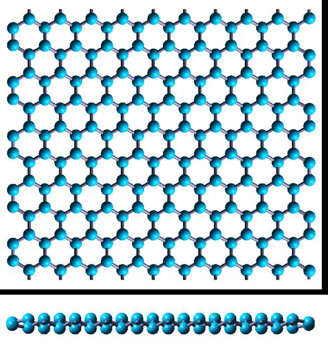
10 Figure 1 (a) The top view and (b) the side view of three-dimensional structure of VA elements. Red arrows are the lattice vectors in the plane. Green rhombus is the unit cell. d is the inter-layer distance.
11 (a) (b) (c) (d) (e) (f) Figure 2 (a) The first Brillouin Zone and the high symmetric points of two-dimensional honeycomb lattice. (b)-(f)band structure evolution of 2-dimensional monolayer of VA elements as it goes from nitrogen to bismuth. Different colors refer to different branches of bands. Fermi energy is set to zero denoted by green dash line.
12 (a) (b) (c) (d) (e) Figure 3 The same as Figure 2, but with SOC. (f)
13 Figure 4 The density of states of monolayers of (a) nigrogen, (b) phosphorus, (c) arsenic, (d) antimony and (e) bismuth. Red, blue and purple solid lines denote the projection into s orbital, p orbital and d orbital, respectively. Fermi energy is set to zero.
14 (a) (b) (c) (d) (e) Figure 5 (a)-(e) Tight-binding band structures of 2-dimensional monolayer of VA elements as it goes from nitrogen to bismuth (red dotted line), compared with first principal results (blue solid line). The first Brillouin Zone and the high symmetric points are the same as two previous figures.
 (d)")


15 (a) (b) (c) (d) (e) (f)

 (b) (c) (d) (e) Figure 7 Band structure of zigzag blue phosphorus ZNR (b) and ANR (c) compared with that of monolayer (a). (d) and (e) Same as (b) and (c), but the energy scale is different.")
16 Figure 6 (a) Schematic drawing of ZNR and ANR with 20 atoms wide. The system is periodic in x direction for ZNR while it is periodic in y direction for ANR. The green and red rectangles represent the atoms in the unit cell for ZNR and ANR, respectively. Vacua of 15 Å are inserted on both sides of the nano-ribbon. (b) and (c) are the optimized structure of ZNR for Nitrogen and Bismuth, respectively. (d), (e) and (f) are the optimized structure of ANR Nitrogen and Bismuth, respectively. (a) (b) (c) (d) (e) Figure 7 Band structure of zigzag blue phosphorus ZNR (b) and ANR (c) compared with that of monolayer (a). (d) and (e) Same as (b) and (c), but the energy scale is different. The Fermi level is denoted by green dash line. Red and blue solid lines in (b) and (d) refer to spin-up and spin-down, respectively.
 and ANR")
 arsenic, (d) antimony")

, (c) and (d), Red and blue")

17 (a) (b) (c) (d) (e) Figure 8 Band structure of ZNR (upper panel) and ANR (lower panel) for (a) nitrogen, (b) phosphorus, (c) arsenic, (d) antimony and (e) bismuth, respectively. The Fermi level is denoted by green dash line. For (b), (c) and (d), Red and blue solid lines refer to spin-up and spin-down, respectively. Figure 9 Charge density distribution of edge state in ZNR of phosphorus.
18 1 Neto A. H. C. et. al. The electronic properties of graphene. Rev. Mod. Phys. 81, 109 (2009) 2 Wang Q. H. et. al. Graphene is not alone. Nat. Nanotech. 7, 683 (2012) 3 Novoselov K. et. al. Two-dimensional atomic crystals. PNAS 102(30), (2005) 4 Neto A. H. C. et. al. Two-Dimensional Crystals: Beyond Graphene. Materials Express 1(1),10 (2011) 5 Butler S. Z. et. al. ACS nano 7(4), 2898 (2013) 6 Castellanos-Gomez A. et. al. Isolation and characterization of few-layer black phosphorus. arxiv: Li L. K. et. al. Black phosphorus field-effect transistors. arxiv: Liu H. et. al., Phosphorene: A New 2D Material with High Carrier Mobility. arxiv: Zhu Z. and Tom ánek D. Semiconducting layered blue phosphorus: A computational study, arxiv: Yukihiro Harada1et. al. Epitaxial two-dimensional nitrogen atomic sheet in GaAs. Appl. Phys. Lett. 104, (2014) 11 Chuang F. C. et. al., Tunable topological electronic structures in Sb(111) bilayers: A firstprinciple study, Appl. Phys. Lett. 102, (2013) 12 Huang Z. Q. et. al., Nontrivial topological electronic structures in a single Bi(111) bilayer on different substrates: A first-principle study. Phys. Rev. B 88, (2013) 13 Perdew J. P., Burke K., and Ernzerhof M. Generalized Gradient Approximation Made Simple. Phys. Rev. Lett. 77, 3865 (1996) 14 Kresse G. and Furthm üller J. Efficient iterative schemes for ab initio total-energy calculations using a plane-wave basis set. Phys. Rev. B 54, (1996) 15 Grimme S. Semiempirical GGA-type density functional constructed with a long-range dispersion correction. J. Comp. Chem 27, 1787 (2006) 16 Klimeš J., Bowler D. R., and Michaelides A. Van der Waals density functionals applied to solids. Phys. Rev. B 83, (2011) 17 Liu H. et. al. Abstract Y at the 2014 March Meeting of the American Physical Society. 18 Cahangirov S., Topsakal M., Aktürk E., Şahin H., and Ciraci S. Two- and One-Dimensional Honeycomb Structures of Silicon and Germanium. Phys. Rev. Lett. 102, (2009) 19 Zólyomi V., Wallbank J. R., Fal'ko V. I. Silicane and germanane: tight-binding and firstprinciples studies. arxiv: v2 20 Liu C. C., Jiang H., and Yao Y. G. Low-energy effective Hamiltonian involving spin-orbit coupling in silicene and two-dimensional germanium and tin. Phys. Rev. B 84, (2011) 21 Okada S. and Oshiyama A. Magnetic Ordering in Hexagonally Bonded Sheets with First-Row Elements. Phys. Rev. Lett., 87, (2001) 22 Bhowmick S. and Shenoy V. B. Edge state magnetism of single layer graphene nanostructures. J. Chem. Phys., 128, (2008) 23
Two-Dimensional Honeycomb Monolayer of Nitrogen Group. Elements and the Related Nano-Structure: A First-Principle Study
 Two-Dimensional Honeycomb Monolayer of Nitrogen Group Elements and the Related Nano-Structure: A First-Principle Study Jason Lee, Wei-Liang Wang, Dao-Xin Yao * State Key Laboratory of Optoelectronic Materials
Band Gap Engineering of Two-Dimensional Nitrogene
 Band Gap Engineering of Two-Dimensional Nitrogene Jie-Sen Li, Wei-Liang Wang, Dao-Xin Yao* State Key Laboratory of Optoelectronic Materials and Technologies, School of Physics, Sun Yat-Sen University,
Tunable Band Gap of Silicene on Monolayer Gallium Phosphide Substrate
 2017 International Conference on Energy Development and Environmental Protection (EDEP 2017) ISBN: 978-1-60595-482-0 Tunable Band Gap of Silicene on Monolayer Gallium Phosphide Substrate Miao-Juan REN
Electronic Structure and Band Gap Engineering of Two-Dimensional Octagon-Nitrogene
 www.nature.com/scientificreports Received: 21 August 2017 Accepted: 3 January 2018 Published: xx xx xxxx OPEN Electronic Structure and Band Gap Engineering of Two-Dimensional Octagon-Nitrogene Wanxing
Effects of biaxial strain on the electronic structures and band. topologies of group-v elemental monolayers
 Effects of biaxial strain on the electronic structures and band topologies of group-v elemental monolayers Jinghua Liang, Long Cheng, Jie Zhang, Huijun Liu * Key Laboratory of Artificial Micro- and Nano-Structures
Two-dimensional octagon-structure monolayer of nitrogen group elements and the related nano-structures
 Two-dimensional octagon-structure monolayer of nitrogen group elements and the related nano-structures Yu Zhang a, Jason Lee a, Wei-Liang Wang a, Dao-Xin Yao a,b* a State Key Laboratory of Optoelectronic
Electronic Supplementary Information
 Electronic Supplementary Material (ESI) for Nanoscale. This journal is The Royal Society of Chemistry 2016 Electronic Supplementary Information Two-dimensional BX (X=P, As, Sb) Semiconductors with Mobilities
Topological band-order transition and quantum spin Hall edge engineering in functionalized X-Bi(111) (X = Ga, In, and Tl) bilayer
 (X = Ga, In, and Tl) bilayer") Supplementary Material Topological band-order transition and quantum spin Hall edge engineering in functionalized X-Bi(111) (X = Ga, In, and Tl) bilayer Youngjae Kim, Won Seok Yun, and J. D. Lee* Department
Supplementary Material Topological band-order transition and quantum spin Hall edge engineering in functionalized X-Bi(111) (X = Ga, In, and Tl) bilayer Youngjae Kim, Won Seok Yun, and J. D. Lee* Department
Puckering and spin orbit interaction in nano-slabs
 Electronic structure of monolayers of group V atoms: Puckering and spin orbit interaction in nano-slabs Dat T. Do* and Subhendra D. Mahanti* Department of Physics and Astronomy, Michigan State University,
Edge effects on the electronic properties of phosphorene nanoribbons
 Edge effects on the electronic properties of phosphorene nanoribbons Xihong Peng, * Qun Wei,, Andrew Copple School of Letters and Sciences, Arizona State University, Mesa, Arizona 8, USA School of Physics
Tinselenidene: a Two-dimensional Auxetic Material with Ultralow Lattice Thermal Conductivity and Ultrahigh Hole Mobility
 Tinselenidene: a Two-dimensional Auxetic Material with Ultralow Lattice Thermal Conductivity and Ultrahigh Hole Mobility Li-Chuan Zhang, Guangzhao Qin, Wu-Zhang Fang, Hui-Juan Cui, Qing-Rong Zheng, Qing-Bo
arxiv: v2 [cond-mat.mtrl-sci] 24 Dec 2014
![arxiv: v2 [cond-mat.mtrl-sci] 24 Dec 2014](/thumbs/93/113232647.jpg "arxiv: v2 [cond-mat.mtrl-sci] 24 Dec 2014") Defect in Phosphorene arxiv:1411.6986v2 [cond-mat.mtrl-sci] 24 Dec 2014 Wei Hu 1, 2, 3, and Jinlong Yang 1 Computational Research Division, Lawrence Berkeley National Laboratory, Berkeley, CA 94720, USA
Defect in Phosphorene arxiv:1411.6986v2 [cond-mat.mtrl-sci] 24 Dec 2014 Wei Hu 1, 2, 3, and Jinlong Yang 1 Computational Research Division, Lawrence Berkeley National Laboratory, Berkeley, CA 94720, USA
Table of Contents. Table of Contents Opening a band gap in silicene and bilayer graphene with an electric field
 Table of Contents Table of Contents Opening a band gap in silicene and bilayer graphene with an electric field Bilayer graphene Building a bilayer graphene structure Calculation and analysis Silicene Optimizing
Physical Properties of Mono-layer of
 Chapter 3 Physical Properties of Mono-layer of Silicene The fascinating physical properties[ 6] associated with graphene have motivated many researchers to search for new graphene-like two-dimensional
arxiv: v3 [cond-mat.mtrl-sci] 4 Mar 2017
![arxiv: v3 [cond-mat.mtrl-sci] 4 Mar 2017](/thumbs/96/128445191.jpg "arxiv: v3 [cond-mat.mtrl-sci] 4 Mar 2017") Transition between strong and weak topological insulator in ZrTe 5 and HfTe 5 Zongjian Fan 1, Qi-Feng Liang 2, Y. B. Chen 3, Shu-Hua Yao 1, and Jian Zhou 1,4,* arxiv:1611.04263v3 [cond-mat.mtrl-sci] 4
Transition between strong and weak topological insulator in ZrTe 5 and HfTe 5 Zongjian Fan 1, Qi-Feng Liang 2, Y. B. Chen 3, Shu-Hua Yao 1, and Jian Zhou 1,4,* arxiv:1611.04263v3 [cond-mat.mtrl-sci] 4
Supplementary Figure S1: Number of Fermi surfaces. Electronic dispersion around Γ a = 0 and Γ b = π/a. In (a) the number of Fermi surfaces is even,
 the number of Fermi surfaces is even,") Supplementary Figure S1: Number of Fermi surfaces. Electronic dispersion around Γ a = 0 and Γ b = π/a. In (a) the number of Fermi surfaces is even, whereas in (b) it is odd. An odd number of non-degenerate
Supplementary Figure S1: Number of Fermi surfaces. Electronic dispersion around Γ a = 0 and Γ b = π/a. In (a) the number of Fermi surfaces is even, whereas in (b) it is odd. An odd number of non-degenerate
ELECTRONIC ENERGY DISPERSION AND STRUCTURAL PROPERTIES ON GRAPHENE AND CARBON NANOTUBES
 ELECTRONIC ENERGY DISPERSION AND STRUCTURAL PROPERTIES ON GRAPHENE AND CARBON NANOTUBES D. RACOLTA, C. ANDRONACHE, D. TODORAN, R. TODORAN Technical University of Cluj Napoca, North University Center of
Supporting Information Tuning Local Electronic Structure of Single Layer MoS2 through Defect Engineering
 Supporting Information Tuning Local Electronic Structure of Single Layer MoS2 through Defect Engineering Yan Chen, 1,2,,$, * Shengxi Huang, 3,6, Xiang Ji, 2 Kiran Adepalli, 2 Kedi Yin, 8 Xi Ling, 3,9 Xinwei
Supporting Information
 Electronic Supplementary Material (ESI) for Nanoscale. This journal is The Royal Society of Chemistry 2015 Supporting Information Single Layer Lead Iodide: Computational Exploration of Structural, Electronic
3-month progress Report
 3-month progress Report Graphene Devices and Circuits Supervisor Dr. P.A Childs Table of Content Abstract... 1 1. Introduction... 1 1.1 Graphene gold rush... 1 1.2 Properties of graphene... 3 1.3 Semiconductor
Transversal electric field effect in multilayer graphene nanoribbon
 Transversal electric field effect in multilayer graphene nanoribbon S. Bala kumar and Jing Guo a) Department of Electrical and Computer Engineering, University of Florida, Gainesville, Florida 32608, USA
Supporting information. Realizing Two-Dimensional Magnetic Semiconductors with. Enhanced Curie Temperature by Antiaromatic Ring Based
 Supporting information Realizing Two-Dimensional Magnetic Semiconductors with Enhanced Curie Temperature by Antiaromatic Ring Based Organometallic Frameworks Xingxing Li and Jinlong Yang* Department of
A comparative computational study of the electronic properties of planar and buckled silicene
 A comparative computational study of the electronic properties of planar and buckled silicene Harihar Behera 1 and Gautam Mukhopadhyay 2 Indian Institute of Technology Bombay, Powai, Mumbai-400076, India
2D MBE Activities in Sheffield. I. Farrer, J. Heffernan Electronic and Electrical Engineering The University of Sheffield
 2D MBE Activities in Sheffield I. Farrer, J. Heffernan Electronic and Electrical Engineering The University of Sheffield Outline Motivation Van der Waals crystals The Transition Metal Di-Chalcogenides
(a) (b) Supplementary Figure 1. (a) (b) (a) Supplementary Figure 2. (a) (b) (c) (d) (e)
 (b) Supplementary Figure 1. (a) (b) (a) Supplementary Figure 2. (a) (b) (c) (d) (e)") (a) (b) Supplementary Figure 1. (a) An AFM image of the device after the formation of the contact electrodes and the top gate dielectric Al 2 O 3. (b) A line scan performed along the white dashed line
(a) (b) Supplementary Figure 1. (a) An AFM image of the device after the formation of the contact electrodes and the top gate dielectric Al 2 O 3. (b) A line scan performed along the white dashed line
Available online at ScienceDirect. Procedia Materials Science 11 (2015 )
") Available online at www.sciencedirect.com ScienceDirect Procedia Materials Science ( ) 9 th International Biennial Conference on Ultrafine Grained and Nanostructured Materials, UFGNSM Doping Effect on
Available online at www.sciencedirect.com ScienceDirect Procedia Materials Science ( ) 9 th International Biennial Conference on Ultrafine Grained and Nanostructured Materials, UFGNSM Doping Effect on
arxiv: v2 [cond-mat.mes-hall] 5 Feb 2015
![arxiv: v2 [cond-mat.mes-hall] 5 Feb 2015](/thumbs/91/106233706.jpg "arxiv: v2 [cond-mat.mes-hall] 5 Feb 2015") Orientation and strain modulated electronic structures in puckered arsenene nanoribbons Z. Y. Zhang, J. C. Zhang, Y. H. Wang, D. S. Xue, and M. S. Si arxiv:1501.06044v2 [cond-mat.mes-hall] 5 Feb 2015 Key
Orientation and strain modulated electronic structures in puckered arsenene nanoribbons Z. Y. Zhang, J. C. Zhang, Y. H. Wang, D. S. Xue, and M. S. Si arxiv:1501.06044v2 [cond-mat.mes-hall] 5 Feb 2015 Key
Band structure engineering of graphene by strain: First-principles calculations
 Band structure engineering of graphene by strain: First-principles calculations Gui Gui, Jin Li, and Jianxin Zhong* Laboratory for Quantum Engineering and Micro-Nano Energy Technology, Xiangtan University,
Structure and Quantum Well States in Silicene Nanoribbons. on Ag(110)
") Structure and Quantum Well States in Silicene Nanoribbons on Ag(110) Baojie Feng 1, Hui Li 1, Sheng Meng 1,2, Lan Chen 1 *, and Kehui Wu 1,2 * 1 Institute of Physics, Chinese Academy of Sciences, Beijing
Structure and Quantum Well States in Silicene Nanoribbons on Ag(110) Baojie Feng 1, Hui Li 1, Sheng Meng 1,2, Lan Chen 1 *, and Kehui Wu 1,2 * 1 Institute of Physics, Chinese Academy of Sciences, Beijing
Supporting information for. Stacking dependent electronic structure and optical properties of bilayer. black phosphorus
 Electronic Supplementary Material (ESI) for Physical Chemistry Chemical Physics. This journal is the Owner Societies 016 Supporting information for Stacking dependent electronic structure and optical properties
Experiment Section Fig. S1 Fig. S2
 Electronic Supplementary Material (ESI) for ChemComm. This journal is The Royal Society of Chemistry 2018 Supplementary Materials Experiment Section The STM experiments were carried out in an ultrahigh
CITY UNIVERSITY OF HONG KONG. Theoretical Study of Electronic and Electrical Properties of Silicon Nanowires
 CITY UNIVERSITY OF HONG KONG Ë Theoretical Study of Electronic and Electrical Properties of Silicon Nanowires u Ä öä ªqk u{ Submitted to Department of Physics and Materials Science gkö y in Partial Fulfillment
The calculation of energy gaps in small single-walled carbon nanotubes within a symmetry-adapted tight-binding model
 The calculation of energy gaps in small single-walled carbon nanotubes within a symmetry-adapted tight-binding model Yang Jie( ) a), Dong Quan-Li( ) a), Jiang Zhao-Tan( ) b), and Zhang Jie( ) a) a) Beijing
CHAPTER 6. ELECTRONIC AND MAGNETIC STRUCTURE OF ZINC-BLENDE TYPE CaX (X = P, As and Sb) COMPOUNDS
 COMPOUNDS") 143 CHAPTER 6 ELECTRONIC AND MAGNETIC STRUCTURE OF ZINC-BLENDE TYPE CaX (X = P, As and Sb) COMPOUNDS 6.1 INTRODUCTION Almost the complete search for possible magnetic materials has been performed utilizing
143 CHAPTER 6 ELECTRONIC AND MAGNETIC STRUCTURE OF ZINC-BLENDE TYPE CaX (X = P, As and Sb) COMPOUNDS 6.1 INTRODUCTION Almost the complete search for possible magnetic materials has been performed utilizing
Electronic properties of aluminium and silicon doped (2, 2) graphyne nanotube
 graphyne nanotube") Journal of Physics: Conference Series PAPER OPEN ACCESS Electronic properties of aluminium and silicon doped (2, 2) graphyne nanotube To cite this article: Jyotirmoy Deb et al 2016 J. Phys.: Conf. Ser.
Journal of Physics: Conference Series PAPER OPEN ACCESS Electronic properties of aluminium and silicon doped (2, 2) graphyne nanotube To cite this article: Jyotirmoy Deb et al 2016 J. Phys.: Conf. Ser.
Defects in TiO 2 Crystals
 , March 13-15, 2013, Hong Kong Defects in TiO 2 Crystals Richard Rivera, Arvids Stashans 1 Abstract-TiO 2 crystals, anatase and rutile, have been studied using Density Functional Theory (DFT) and the Generalized
A model for the direct-to-indirect band-gap transition in monolayer MoSe 2 under strain
 PRAMANA c Indian Academy of Sciences Vol. 84, No. 6 journal of June 25 physics pp. 33 4 A model for the direct-to-indirect band-gap transition in monolayer MoSe 2 under strain RUMA DAS and PRIYA MAHADEVAN
This manuscript was submitted first in a reputed journal on Apri1 16 th Stanene: Atomically Thick Free-standing Layer of 2D Hexagonal Tin
 This manuscript was submitted first in a reputed journal on Apri1 16 th 2015 Stanene: Atomically Thick Free-standing Layer of 2D Hexagonal Tin Sumit Saxena 1, Raghvendra Pratap Choudhary, and Shobha Shukla
Supplementary Figure S1. STM image of monolayer graphene grown on Rh (111). The lattice
. The lattice") Supplementary Figure S1. STM image of monolayer graphene grown on Rh (111). The lattice mismatch between graphene (0.246 nm) and Rh (111) (0.269 nm) leads to hexagonal moiré superstructures with the expected
Supplementary Figure S1. STM image of monolayer graphene grown on Rh (111). The lattice mismatch between graphene (0.246 nm) and Rh (111) (0.269 nm) leads to hexagonal moiré superstructures with the expected
Supplementary Information
 Supplementary Information Supplementary Figure 1: Electronic Kohn-Sham potential profile of a charged monolayer MoTe 2 calculated using PBE-DFT. Plotted is the averaged electronic Kohn- Sham potential
Dumbbell Stanane: A large-gap quantum spin Hall insulator
 Dumbbell Stanane: A large-gap quantum spin Hall insulator Xin Chen, Linyang Li, Mingwen Zhao* School of Physics and State Key Laboratory of Crystal Materials, Shandong University, Jinan, Shandong, 250100,
arxiv: v1 [cond-mat.mes-hall] 23 Oct 2014
![arxiv: v1 [cond-mat.mes-hall] 23 Oct 2014](/thumbs/89/98938212.jpg "arxiv: v1 [cond-mat.mes-hall] 23 Oct 2014") Unusual Electronic Structure of Few-Layer Grey Arsenic: A Computational Study Zhen Zhu, Jie Guan, and David Tománek Physics and Astronomy Department, Michigan State University, East Lansing, Michigan 4884,
Unusual Electronic Structure of Few-Layer Grey Arsenic: A Computational Study Zhen Zhu, Jie Guan, and David Tománek Physics and Astronomy Department, Michigan State University, East Lansing, Michigan 4884,
Supporting Information. Enhanced Raman Scattering on In-Plane Anisotropic Layered Materials
 Supporting Information Enhanced Raman Scattering on In-Plane Anisotropic Layered Materials Jingjing Lin 1, Liangbo Liang 2,3, Xi Ling 4, Shuqing Zhang 1, Nannan Mao 1, Na Zhang 1, Bobby G. Sumpter 2,5,
Theoretical Concepts of Spin-Orbit Splitting
 Chapter 9 Theoretical Concepts of Spin-Orbit Splitting 9.1 Free-electron model In order to understand the basic origin of spin-orbit coupling at the surface of a crystal, it is a natural starting point
SnO 2 Physical and Chemical Properties due to the Impurity Doping
 , March 13-15, 2013, Hong Kong SnO 2 Physical and Chemical Properties due to the Impurity Doping Richard Rivera, Freddy Marcillo, Washington Chamba, Patricio Puchaicela, Arvids Stashans Abstract First-principles
This article is available at IRis:
 Author(s) D. Hsieh, Y. Xia, D. Qian, L. Wray, F. Meier, J. H. Dill, J. Osterwalder, L. Patthey, A. V. Fedorov, H. Lin, A. Bansil, D. Grauer, Y. S. Hor, R. J. Cava, and M. Z. Hasan This article is available
arxiv: v1 [cond-mat.mes-hall] 15 Aug 2014
![arxiv: v1 [cond-mat.mes-hall] 15 Aug 2014](/thumbs/89/97831186.jpg "arxiv: v1 [cond-mat.mes-hall] 15 Aug 2014") The potential applications of phosphorene as anode arxiv:1408.3488v1 [cond-mat.mes-hall] 15 Aug 2014 materials in Li-ion batteries Shijun Zhao,, and Wei Kang, HEDPS, Center for Applied Physics and Technology,
The potential applications of phosphorene as anode arxiv:1408.3488v1 [cond-mat.mes-hall] 15 Aug 2014 materials in Li-ion batteries Shijun Zhao,, and Wei Kang, HEDPS, Center for Applied Physics and Technology,
Electronic structure and properties of a few-layer black phosphorus Mikhail Katsnelson
 Electronic structure and properties of a few-layer black phosphorus Mikhail Katsnelson Main collaborators: Sasha Rudenko Shengjun Yuan Rafa Roldan Milton Pereira Sergey Brener Motivation Plenty of 2D materials
arxiv: v2 [cond-mat.mtrl-sci] 25 Jan 2010
![arxiv: v2 [cond-mat.mtrl-sci] 25 Jan 2010](/thumbs/76/73887967.jpg "arxiv: v2 [cond-mat.mtrl-sci] 25 Jan 2010") A First-Principles Study of Zinc Oxide Honeycomb Structures arxiv:0907.3070v2 [cond-mat.mtrl-sci] 25 Jan 2010 M. Topsakal, 1 S. Cahangirov, 1 E. Bekaroglu, 1 and S. Ciraci 1, 2 1 UNAM-Institute of Materials
A First-Principles Study of Zinc Oxide Honeycomb Structures arxiv:0907.3070v2 [cond-mat.mtrl-sci] 25 Jan 2010 M. Topsakal, 1 S. Cahangirov, 1 E. Bekaroglu, 1 and S. Ciraci 1, 2 1 UNAM-Institute of Materials
Supplementary Information
 Supplementary Information Supplementary Figure S1: Ab initio band structures in presence of spin-orbit coupling. Energy bands for (a) MoS 2, (b) MoSe 2, (c) WS 2, and (d) WSe 2 bilayers. It is worth noting
and strong interlayer quantum confinement
 Supporting Information GeP3: A small indirect band gap 2D crystal with high carrier mobility and strong interlayer quantum confinement Yu Jing 1,3, Yandong Ma 1, Yafei Li 2, *, Thomas Heine 1,3 * 1 Wilhelm-Ostwald-Institute
arxiv: v2 [cond-mat.mtrl-sci] 21 Apr 2014
![arxiv: v2 [cond-mat.mtrl-sci] 21 Apr 2014](/thumbs/85/92449877.jpg "arxiv: v2 [cond-mat.mtrl-sci] 21 Apr 2014") Peierls transition and edge reconstruction in phosphorene nanoribbons Ajanta Maity, Akansha Singh, and Prasenjit Sen,a) Harish-Chandra Research Institute, Chhatnag Road, Jhunsi, Allahabad 9, India. arxiv:44.469v
Peierls transition and edge reconstruction in phosphorene nanoribbons Ajanta Maity, Akansha Singh, and Prasenjit Sen,a) Harish-Chandra Research Institute, Chhatnag Road, Jhunsi, Allahabad 9, India. arxiv:44.469v
Construction of Two Dimensional Chiral Networks
 Supporting Information Construction of Two Dimensional Chiral Networks through Atomic Bromine on Surfaces Jianchen Lu, De-Liang Bao, Huanli Dong, Kai Qian, Shuai Zhang, Jie Liu, Yanfang Zhang, Xiao Lin
CO Adsorption Site Preference on Platinum: Charge Is the Essence
 Supporting Information CO Adsorption Site Preference on Platinum: Charge Is the Essence G.T. Kasun Kalhara Gunasooriya, and Mark Saeys *, Laboratory for Chemical Technology, Ghent University, Technologiepark
Edinburgh Research Explorer
 Edinburgh Research Explorer Hydrogenation induced carrier mobility polarity reversal in single layer AlN Citation for published version: Ackland, G & Zong, H 2017, 'Hydrogenation induced carrier mobility
Lectures Graphene and
 Lectures 15-16 Graphene and carbon nanotubes Graphene is atomically thin crystal of carbon which is stronger than steel but flexible, is transparent for light, and conducts electricity (gapless semiconductor).
Supporting Information: Local Electronic Structure of a Single-Layer. Porphyrin-Containing Covalent Organic Framework
 Supporting Information: Local Electronic Structure of a Single-Layer Porphyrin-Containing Covalent Organic Framework Chen Chen 1, Trinity Joshi 2, Huifang Li 3, Anton D. Chavez 4,5, Zahra Pedramrazi 2,
SUPPLEMENTARY INFORMATION
 Atomic structure and dynamic behaviour of truly one-dimensional ionic chains inside carbon nanotubes Ryosuke Senga 1, Hannu-Pekka Komsa 2, Zheng Liu 1, Kaori Hirose-Takai 1, Arkady V. Krasheninnikov 2
SUPPLEMENTARY INFORMATION
 A Dirac point insulator with topologically non-trivial surface states D. Hsieh, D. Qian, L. Wray, Y. Xia, Y.S. Hor, R.J. Cava, and M.Z. Hasan Topics: 1. Confirming the bulk nature of electronic bands by
Hydrogenation of Penta-Graphene Leads to Unexpected Large. Improvement in Thermal Conductivity
 Supplementary information for Hydrogenation of Penta-Graphene Leads to Unexpected Large Improvement in Thermal Conductivity Xufei Wu, a Vikas Varshney, b,c Jonghoon Lee, b,c Teng Zhang, a Jennifer L. Wohlwend,
PBS: FROM SOLIDS TO CLUSTERS
 PBS: FROM SOLIDS TO CLUSTERS E. HOFFMANN AND P. ENTEL Theoretische Tieftemperaturphysik Gerhard-Mercator-Universität Duisburg, Lotharstraße 1 47048 Duisburg, Germany Semiconducting nanocrystallites like
Supporting Information for Ultra-narrow metallic armchair graphene nanoribbons
 Supporting Information for Ultra-narrow metallic armchair graphene nanoribbons Supplementary Figure 1 Ribbon length statistics. Distribution of the ribbon lengths and the fraction of kinked ribbons for
Supporting information for Polymer interactions with Reduced Graphene Oxide: Van der Waals binding energies of Benzene on defected Graphene
 Supporting information for Polymer interactions with Reduced Graphene Oxide: Van der Waals binding energies of Benzene on defected Graphene Mohamed Hassan, Michael Walter *,,, and Michael Moseler, Freiburg
Introduction of XPS Absolute binding energies of core states Applications to silicone Outlook
 Core level binding energies in solids from first-principles Introduction of XPS Absolute binding energies of core states Applications to silicone Outlook TO and C.-C. Lee, Phys. Rev. Lett. 118, 026401
Our first-principles calculations were performed using the Vienna Ab Initio Simulation
 Supplementary Note 1: Computational details First-principles calculations Our first-principles calculations were performed using the Vienna Ab Initio Simulation Package (VASP) 1, which is based on density
Novel Phases of Semi-Conducting Silicon Nitride Bilayer: A First-Principle Study
 Novel Phases of Semi-Conducting Silicon Nitride Bilayer: A First-Principle Study Jiesen Li 1, Wanxing Lin 2, Junjun Shi 1, Feng Zhu 1, Weiliang Wang 2, Haiwen Xie 1, Dao-Xin Yao* 2 1 School of Environment
From Graphene to Nanotubes
 From Graphene to Nanotubes Zone Folding and Quantum Confinement at the Example of the Electronic Band Structure Christian Krumnow christian.krumnow@fu-berlin.de Freie Universität Berlin June 6, Zone folding
Band engineering of Dirac surface states in topological insulators-based van. der Waals heterostructures
 Band engineering of Dirac surface states in topological insulators-based van der Waals heterostructures Cui-Zu Chang, 1, 2 Peizhe Tang, 1 Xiao Feng, 1, 2 Kang Li, 2 Xu-Cun Ma, 1 Wenhui Duan, 1,3 Ke He,
Structural, electronic and magnetic properties of vacancies in single-walled carbon nanotubes
 Structural, electronic and magnetic properties of vacancies in single-walled carbon nanotubes W. Orellana and P. Fuentealba Departamento de Física, Facultad de Ciencias, Universidad de Chile, Casilla 653,
SUPPLEMENTARY INFORMATION
 In the format provided by the authors and unedited. DOI: 10.1038/NPHYS3968 Topological mosaic in Moiré superlattices of van der Waals heterobilayers Qingjun Tong 1, Hongyi Yu 1, Qizhong Zhu 1, Yong Wang
SUPPLEMENTARY INFORMATION
 A Stable Three-dimensional Topological Dirac Semimetal Cd 3 As 2 Z. K. Liu, J. Jiang, B. Zhou, Z. J. Wang, Y. Zhang, H. M. Weng, D. Prabhakaran, S. -K. Mo, H. Peng, P. Dudin, T. Kim, M. Hoesch, Z. Fang,
Supporting Information
 Supporting Information Ultrathin Spinel-Structured Nanosheets Rich in Oxygen Deficiencies for Enhanced Electrocatalytic Water Oxidation** Jian Bao, Xiaodong Zhang,* Bo Fan, Jiajia Zhang, Min Zhou, Wenlong
Large-gap quantum spin Hall state in functionalized dumbbell stanene
 Large-gap quantum spin Hall state in functionalized dumbbell stanene Ya-ping Wang, a Wei-xiao Ji, a Chang-wen Zhang*, a Ping Li, a Feng Li, a Pei-ji Wang, a Sheng-shi Li, b Shi-shen Yan b a School of Physics
Regulating Intrinsic Defects and Substrate Transfer Doping
 Fermi Level Tuning of Epitaxial Sb 2 Te 3 Thin Films on Graphene by Regulating Intrinsic Defects and Substrate Transfer Doping Yeping Jiang, 1,2 Y. Y. Sun, 3 Mu Chen, 1,2 Yilin Wang, 1 Zhi Li, 1 Canli
Monolayer hexagonal arsenene with tunable electronic structures and. magnetic properties via impurity doping
 Monolayer hexagonal arsenene with tunable electronic structures and magnetic properties via impurity doping Zhongjun Li, a Wei Xu, a Yuanqin Yu, b Hongyang Du, a Kun Zhen, a Jun Wang, a Linbao Luo,* a
Graphene and Planar Dirac Equation
 Graphene and Planar Dirac Equation Marina de la Torre Mayado 2016 Marina de la Torre Mayado Graphene and Planar Dirac Equation June 2016 1 / 48 Outline 1 Introduction 2 The Dirac Model Tight-binding model
Black phosphorus: A new bandgap tuning knob
 Black phosphorus: A new bandgap tuning knob Rafael Roldán and Andres Castellanos-Gomez Modern electronics rely on devices whose functionality can be adjusted by the end-user with an external knob. A new
An Extended Hückel Theory based Atomistic Model for Graphene Nanoelectronics
 Journal of Computational Electronics X: YYY-ZZZ,? 6 Springer Science Business Media, Inc. Manufactured in The Netherlands An Extended Hückel Theory based Atomistic Model for Graphene Nanoelectronics HASSAN
arxiv: v1 [cond-mat.mes-hall] 25 Jun 2013
![arxiv: v1 [cond-mat.mes-hall] 25 Jun 2013](/thumbs/85/91564485.jpg "arxiv: v1 [cond-mat.mes-hall] 25 Jun 2013") Effects of charging and electric field on the properties of silicene and germanene H. Hakan Gürel, 1, 2, 3 V. Ongun Özçelik,1, 2 1, 2, 4, and S. Ciraci 1 UNAM-National Nanotechnology Research Center, arxiv:1306.5891v1
Effects of charging and electric field on the properties of silicene and germanene H. Hakan Gürel, 1, 2, 3 V. Ongun Özçelik,1, 2 1, 2, 4, and S. Ciraci 1 UNAM-National Nanotechnology Research Center, arxiv:1306.5891v1
Supporting Information for
 Supporting Information for Pb-activated Amine-assisted Photocatalytic Hydrogen Evolution Reaction on Organic-Inorganic Perovskites Lu Wang *,,, Hai Xiao, Tao Cheng, Youyong Li *,, William A. Goddard III
Selectivity in the initial C-H bond cleavage of n-butane on PdO(101)
") Supporting Information for Selectivity in the initial C-H bond cleavage of n-butane on PdO(101) Can Hakanoglu (a), Feng Zhang (a), Abbin Antony (a), Aravind Asthagiri (b) and Jason F. Weaver (a) * (a)
Supporting Information for Selectivity in the initial C-H bond cleavage of n-butane on PdO(101) Can Hakanoglu (a), Feng Zhang (a), Abbin Antony (a), Aravind Asthagiri (b) and Jason F. Weaver (a) * (a)
Chemical Modification of Silicene *
 Chemical Modification of Silicene * Rong Wang ( 王蓉 ), 1 Mingsheng Xu ( 徐明生 ) 2 & Xiaodong Pi ( 皮孝东 ) 3 1 Key Laboratory of Interface Science and Engineering in Advanced Materials, Ministry of Education,
SUPPLEMENTARY FIGURES
 1 SUPPLEMENTARY FIGURES Supplementary Figure 1: Initial stage showing monolayer MoS 2 islands formation on Au (111) surface. a, Scanning tunneling microscopy (STM) image of molybdenum (Mo) clusters deposited
Solid State Communications
 Solid State Communications 152 (2012) 1089 1093 Contents lists available at SciVerse ScienceDirect Solid State Communications journal homepage: www.elsevier.com/locate/ssc Fast-track Communication First-principle
DFT EXERCISES. FELIPE CERVANTES SODI January 2006
 DFT EXERCISES FELIPE CERVANTES SODI January 2006 http://www.csanyi.net/wiki/space/dftexercises Dr. Gábor Csányi 1 Hydrogen atom Place a single H atom in the middle of a largish unit cell (start with a
Theoretical Study on Carrier Mobility of Hydrogenated Graphene/Hexagonal Boron-Nitride Heterobilayer
 Ye et al. Nanoscale Research Letters (2018) 13:376 https://doi.org/10.1186/s11671-018-2780-2 NANO EXPRESS Theoretical Study on Carrier Mobility of Hydrogenated Graphene/Hexagonal Boron-Nitride Heterobilayer
First-principles study of zinc oxide honeycomb structures
 PHYSICAL REVIEW B 8, 235119 29 First-principles study of zinc oxide honeycomb structures M. Topsakal, 1 S. Cahangirov, 1 E. Bekaroglu, 1 and S. Ciraci 1,2 1 UNAM-Institute of Materials Science and Nanotechnology,
Conductance of Graphene Nanoribbon Junctions and the Tight Binding Model
 Wu and Childs Nanoscale es Lett, 6:6 http://www.nanoscalereslett.com/content/6//6 NANO EXPE Open Access Conductance of Graphene Nanoribbon Junctions and the Tight Binding Model Y Wu, PA Childs * Abstract
GRAPHENE NANORIBBONS TRANSPORT PROPERTIES CALCULATION. Jan VOVES
 GRAPHENE NANORIBBONS TRANSPORT PROPERTIES CALCULATION Jan VOVES Czech Technical University in Prague, Faculty of Electrical Engineering, Technicka 2, CZ-16627 Prague 6 Czech Republic, voves@fel.cvut.cz
arxiv: v1 [cond-mat.mes-hall] 17 Jan 2013
![arxiv: v1 [cond-mat.mes-hall] 17 Jan 2013](/thumbs/92/108463391.jpg "arxiv: v1 [cond-mat.mes-hall] 17 Jan 2013") Electrically Tunable Topological State in [111] Perovskite Materials with Antiferromagnetic Exchange Field Qi-Feng Liang, 1,2 Long-Hua Wu, 1 and Xiao Hu 1 1 International Center for Materials Nanoarchitectornics
Electrically Tunable Topological State in [111] Perovskite Materials with Antiferromagnetic Exchange Field Qi-Feng Liang, 1,2 Long-Hua Wu, 1 and Xiao Hu 1 1 International Center for Materials Nanoarchitectornics
Strain-induced energy band gap opening in two-dimensional bilayered silicon film
 Strain-induced energy band gap opening in two-dimensional bilayered silicon film Z. Ji 1, R. Zhou 2, L. C. Lew Yan Voon 3, Y. Zhuang 1 1 Department of Electrical Engineering, Wright State University, Dayton,
Strong Facet-Induced and Light-Controlled Room-Temperature. Ferromagnetism in Semiconducting β-fesi 2 Nanocubes
 Supporting Information for Manuscript Strong Facet-Induced and Light-Controlled Room-Temperature Ferromagnetism in Semiconducting β-fesi 2 Nanocubes Zhiqiang He, Shijie Xiong, Shuyi Wu, Xiaobin Zhu, Ming
Supplementary Figure 1. Selected area electron diffraction (SAED) of bilayer graphene and tblg. (a) AB
 of bilayer graphene and tblg. (a) AB") Supplementary Figure 1. Selected area electron diffraction (SAED) of bilayer graphene and tblg. (a) AB stacked bilayer graphene (b), (c), (d), (e), and (f) are twisted bilayer graphene with twist angle
Supplementary Figure 1. Selected area electron diffraction (SAED) of bilayer graphene and tblg. (a) AB stacked bilayer graphene (b), (c), (d), (e), and (f) are twisted bilayer graphene with twist angle
Epitaxial graphene on SiC(0001): More than just honeycombs. Y. Qi, S. H. Rhim, G. F. Sun, M. Weinert, and L. Li*
: More than just honeycombs. Y. Qi, S. H. Rhim, G. F. Sun, M. Weinert, and L. Li*") Epitaxial graphene on SiC(0001): More than just honeycombs Y. Qi, S. H. Rhim, G. F. Sun, M. Weinert, and L. Li* Department of Physics and Laboratory for Surface Studies University of Wisconsin, Milwaukee,
Epitaxial graphene on SiC(0001): More than just honeycombs Y. Qi, S. H. Rhim, G. F. Sun, M. Weinert, and L. Li* Department of Physics and Laboratory for Surface Studies University of Wisconsin, Milwaukee,
arxiv: v2 [cond-mat.mtrl-sci] 10 Jul 2018
![arxiv: v2 [cond-mat.mtrl-sci] 10 Jul 2018](/thumbs/81/84557778.jpg "arxiv: v2 [cond-mat.mtrl-sci] 10 Jul 2018") Linear response phonon dynamics of anisotropic black phosphorous monolayer: PAW mediated ab initio DFPT calculations Sushant Kumar Behera and Pritam Deb Advanced Functional Material Laboratory, Department
Linear response phonon dynamics of anisotropic black phosphorous monolayer: PAW mediated ab initio DFPT calculations Sushant Kumar Behera and Pritam Deb Advanced Functional Material Laboratory, Department
arxiv: v1 [cond-mat.mes-hall] 1 Nov 2011
![arxiv: v1 [cond-mat.mes-hall] 1 Nov 2011](/thumbs/93/111880633.jpg "arxiv: v1 [cond-mat.mes-hall] 1 Nov 2011") V The next nearest neighbor effect on the D materials properties Maher Ahmed Department of Physics and Astronomy, University of Western Ontario, London ON N6A K7, Canada and arxiv:.v [cond-mat.mes-hall]
V The next nearest neighbor effect on the D materials properties Maher Ahmed Department of Physics and Astronomy, University of Western Ontario, London ON N6A K7, Canada and arxiv:.v [cond-mat.mes-hall]
Supplementary Materials for Oxygen-induced self-assembly of quaterphenyl molecule on metal surfaces
 Electronic Supplementary Material (ESI) for ChemComm. This journal is The Royal Society of Chemistry 2014 Supplementary Materials for Oxygen-induced self-assembly of quaterphenyl molecule on metal surfaces
Co-existing honeycomb and Kagome characteristics. in the electronic band structure of molecular. graphene: Supporting Information
 Co-existing honeycomb and Kagome characteristics in the electronic band structure of molecular graphene: Supporting Information Sami Paavilainen,, Matti Ropo,, Jouko Nieminen, Jaakko Akola,, and Esa Räsänen
Supplementary information: Topological Properties Determined by Atomic Buckling in Self-Assembled Ultrathin Bi (110)
") Supplementary information: Topological Properties Determined by Atomic Buckling in Self-Assembled Ultrathin Bi (110) Yunhao Lu, *,, Wentao Xu, Mingang Zeng, Guanggeng Yao, Lei Shen, Ming Yang, Ziyu Luo,
Supplementary information: Topological Properties Determined by Atomic Buckling in Self-Assembled Ultrathin Bi (110) Yunhao Lu, *,, Wentao Xu, Mingang Zeng, Guanggeng Yao, Lei Shen, Ming Yang, Ziyu Luo,
CHAPTER 6 CHIRALITY AND SIZE EFFECT IN SINGLE WALLED CARBON NANOTUBES
 10 CHAPTER 6 CHIRALITY AND SIZE EFFECT IN SINGLE WALLED CARBON NANOTUBES 6.1 PREAMBLE Lot of research work is in progress to investigate the properties of CNTs for possible technological applications.