Table of Contents. Table of Contents Opening a band gap in silicene and bilayer graphene with an electric field
|
|
|
- Laura Newton
- 5 years ago
- Views:
Transcription
1 Table of Contents Table of Contents Opening a band gap in silicene and bilayer graphene with an electric field Bilayer graphene Building a bilayer graphene structure Calculation and analysis Silicene Optimizing the geometry Band structure References More reading
2 QuantumATK Try it! QuantumATK Contact Docs» Tutorials» Graphene and other 2D materials» Opening a band gap in silicene and bilayer graphene with an electric field Opening a band gap in silicene and bilayer graphene with an electric field Version: 2017 Downloads & Links PDF Introduction to QuantumATK ATK Reference Manual In this tutorial you will learn how to insert metallic gate electrodes in an QuantumATK bulk calculation and use them to apply electric fields. You will use these features to study the opening of a band gap in bilayer graphene and in silicene under the presence of an electric field. It is assumed that you are familiar with the basic functionalities of QuantumATK. Bilayer graphene Building a bilayer graphene structure 1. Create a new empty project and open Builder (icon ). 2. Insert graphite (not graphene!) from Database. 3. Open Bulk Tools Lattice Parameters. Select Cartesian coordinates and set the value of c lattice constant to be 25 Å.
3

4 4. Go to Coordinate Tools Center and click Appy to center the system.
.")
5 5. To insert the metal electrodes, open Miscellaneous Spatial Regions..., right-click the table (the area under the headers Region Type/Value) and click Insert region twice. 6. Set the voltage to 0 V for the first metallic region, and 10 V for the second. Change their size so that they cover the entire hexagonal unit cell (see the figure below). It does not matter if the regions stick outside the cell, those parts will be ignored in the calculation anyway.

6 The applied voltage results in 4 V/nm in the z direction, just above the field that has been found in experiments to open a band gap. Calculation and analysis We will then analyze the band structure of the graphene bilayer under the static electric field. 1. Send the graphene bilayer structure to Script Generator. 2. Insert a New Calculator block

7 3. Open the New Calculator block, and choose the ATK-SE: Extended Hückel method. For good accuracy, set the k-points to be 9x9x1. 4. Under Huckel basis set select the Cerda. Carbon [graphite] basis set, which describes the sp2 bonding of graphene very well. 5. Untick the No SCF iteration option to carry out the computation self-consistently.

8 Warning It is extremely important to include self-selconsistency; otherwise the field will not have any effect at all! 6. Go to Poisson solver, set Multi-grid in Solver, and choose Dirichlet in Boundary Conditioins on both sides in the C direction. Note For this particular calculation, you can choose any boundary condition in the C direction since the metal gates will fix the potential at the boundaries anyway, but Dirichlet is the physically correct condition when a constant value of the potential is desired at the boundary. 7. Add a Bandstructure block by clicking Analysis Bandstructure.


9 8. Double-click the Bandstructure block and change the route to G, M, K, G. Also increase the number of points per segment to 200.
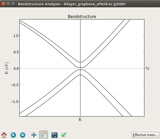
10 9. Name the output file bilayer_graphene_efield.nc. 10. Send the calculation to Job Manager, save the Python script in the window that appears and run the calculation. It should take no more than seconds to run. After the calculation, visualize the band structure and zoom in around the K point, where a band gap is opening with increasing the strength of the electric field. The following figures, from top to bottom, show the band structure of the bilayer graphene with an applied electric field of 0, 10, and 20 Volts, respectively.

11
12

13 Note You can use DFT as well, the results will be similar. No attention was paid to the interlayer distance. You can change it a bit to see how the band structure changes. Note, however, that you cannot use DFT/GGA to optimize this distance because no energy minimum will be found, due to the absence of dispersion corrections (the layers are bound by Van der Waals forces, not captured in standard GGA). LDA works, fortuitously, because of a cancellation of errors, but the results cannot really be trusted. Silicene To study the effect of electric fields on silicene you first need a good model of this material. The approach will be to start with graphene and turn it into silicene, optimize the geometry, and then repeat the same steps followed to calculate the bilayer graphene under the presence of an electric field.
 and using the Periodic Table tool. 3.")
14 Optimizing the geometry 1. In Builder, add graphene (not graphite this time) from Database to Stash following the same steps explained above for the bilayer graphene. 2. Change the two C atoms to Si by selecting them (using the left mouse button while holding down the Ctrl button of your keyboard) and using the Periodic Table tool. 3. The lattice constant of silicene is not the same as for graphene, but rather than guess it, it will simply be part of the geometry optimization to determine it. To start from a reasonable guess, click Bulk Tools Lattice Parameters. Make sure to keep the fractional coordinates constant, set the lattice parameter a to be 3.8 Å and increase the c lattice parameter to 20 Å.
15 4. In Builder, go to Coordinate Tools Center, in order to center the configuration. 5. The flat geometry where both Si atoms are in the same plane is a local minimum in the potential energy surface. Therefore, click the Rattle tool a few times to add a small perturbation to the coordinates. This ensures that the geometry optimization will converge to the global minimum. 6. Send the geometry to Script Generator by using the Send To button. 7. In Script Generator, insert New Calculator and OptimizeGeometry blocks by double-clicking the icons in the Blocks panel:

16 New Calculator. Optimization OptimizeGeometry. 8. Use 21x21x1 k-points for good accuracy, and choose GGA-PBE for exchange-correlation. You can in principle use the default DoubleZetaPolarized basis set, but here you will use the Tight Tier 1 basis set, which provides slightly better results. 9. In the OptimizeGeometry block, set the force tolerance to be small (0.01 ev/å) and the stress tolerance to be even smaller ( ev/å 3). Unconstrain the cell in the x and y directions.

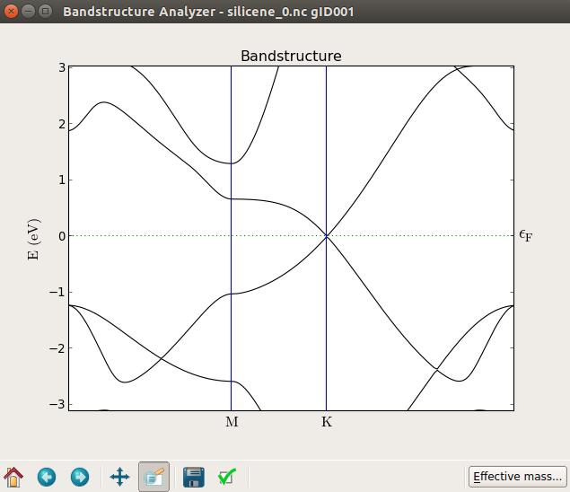
17 10. Name the output file silicene_optimize.nc and save the Python script. 11. Send the script to Job Manager, save the script and run the job. The calculation will take about 10 minutes. When it finishes, drop the Bulk Configuration with ID gid001 on Builder, and inspect the geometry. You will find a nicely optimized silicene sheet with a buckling of about 0.5 Å and an optimized lattice constant of 3.86 Å. Both values are in good agreement with those reported in the literature [1-2]. Band structure Using the optimized structure, repeat the steps above for the bilayer graphene to insert metallic gates and compute the band structure with electric fields. Notice that, in the case of silicene, you need to make the spatial region larger in the XY plane, since the cell is also larger. Use 20 V as the voltage on the second electrode.
 and with 20 V applied on the gate (bottom), which produces a band gap of about 0.1 ev.")
18 Note You should use the same calculator settings as for the optimization. The calculation will take less than a minute. In the plot below you can see the band structure at zero field (top) and with 20 V applied on the gate (bottom), which produces a band gap of about 0.1 ev. By trying different values of the voltage you will find that the band gap increases essentially linearly with the field as shown in [3].
19

20 Notice that in this case, if you look closely, the band gap is not exactly at the K point. Note If you apply a transverse field to a single graphene layer, no gap opens up. The reason is that the graphene is completely flat, and so the field just gives a constant shift of the potential. In the case of silicene the gap appears because the sheet is naturally bukled. References [1] S. Cahangirov, M. Topsakal, E. Akturk, H. Sahin, and S. Ciraci, Two- and One-Dimensional Honeycomb Structures of Silicon and Germanium, Physical Review Letters 102, (2009) [2] N. D. Drummond, V. Zolyomi, and V. I. Fal ko, Electrically tunable band gap in silicene, Physical Review B 85, (2012) [3] R. Zhou, Structural And Electronic Properties of Two-Dimensional Silicene, Graphene, and Related Structures, Master Thesis, Wright State University, Electrical Engineering, Dayton OH, USA (2012) More reading Z. Ni et al., Tunable Bandgap in Silicene and Germanene, Nano Letters 12, (2011) C. Xu et al., Giant magnetoresistance in silicene nanoribbons, Nanoscale 4, (2012)
21 Y. Wang et al., Half-metallic Silicene And Germanene Nanoribbons. Towards High-performance Spintronics Device, Nano 7, (2012) L. Pan et al., Thermoelectric properties of armchair and zigzag silicene nanoribbons, Phys. Chem. Chem. Phys. 14, (2012) H. Li et al., High performance silicene nanoribbon field effect transistors with current saturation, European Physical Journal B 85, 1 (2012) R. Quhe et al., Tunable and sizable band gap in silicene by surface adsorption, Sci. Rep. 2, 853 (2012) For a similar study on hexagonal boron-nitride (hbn), see K. Tang et al., Electronic and transport properties of a biased multilayer hexagonal boron nitride, European Physical Journal B 85, 301 (2012) Copyright 2018, Synopsys Denmark.
QuantumWise. QuantumWise is now part of Synopsys
 Table of Contents Table of Contents NiSi2 Si interface Create the NiSi2/Si device The screening region Increase the length of the central region Set-up the calculation for the undoped device Dope the device
Phonons: Bandstructure, thermal transport, thermo-electrics
 Phonons: Bandstructure, thermal transport, thermo-electrics Tutorial Version 2014.0 Phonons: Bandstructure, thermal transport, thermo-electrics: Tutorial Version 2014.0 Copyright 2008 2014 QuantumWise
Table of Contents. Table of Contents Spin-orbit splitting of semiconductor band structures
 Table of Contents Table of Contents Spin-orbit splitting of semiconductor band structures Relavistic effects in Kohn-Sham DFT Silicon band splitting with ATK-DFT LSDA initial guess for the ground state
Table of Contents. Table of Contents Exploring graphene. Build a graphene sheet Build a CNT Transmission spectrum of a GNR Twisted nanoribbon
 Table of Contents Table of Contents Exploring graphene Build a graphene sheet Build a CNT Transmission spectrum of a GNR Twisted nanoribbon Transmission spectrum Möbius nanoribbon Buckling a graphene sheet
Table of Contents. Table of Contents Phonon-limited mobility in graphene using the Boltzmann transport equation
 Table of Contents Table of Contents Phonon-limited mobility in graphene using the Boltzmann transport equation Geometry and electronic structure of graphene Phonons in Graphene Mobility of graphene 1.
Table of Contents. Table of Contents Electronic structure of NiO with DFT+U. Introduction The electronic structure of NiO calculated with DFT
 Table of Contents Table of Contents Electronic structure of NiO with DFT+U Introduction The electronic structure of NiO calculated with DFT Setting up the calculation Performing the calculation Analysing
Table of Contents. Table of Contents Using the Crystal Builder. Introduction Crystal structure of black phosphorus Phosphorene and its bandstructure
 Table of Contents Table of Contents Using the Crystal Builder Introduction Crystal structure of black phosphorus Phosphorene and its bandstructure Bandstructure References 1 2 2 3 7 9 10 QuantumATK Try
Table of Contents. Table of Contents Computing the piezoelectric tensor for AlN. Introduction. Computing the piezoelectric tensor
 Table of Contents Table of Contents Computing the piezoelectric tensor for AlN Introduction The piezoelectric tensor Computing the piezoelectric tensor Analysis of the e 33 e33 coefficient Alternative
Table of Contents. Table of Contents DFT-1/2 and DFT-PPS density functional methods for electronic structure calculations
 Table of Contents Table of Contents DFT-1/2 and DFT-PPS density functional methods for electronic structure calculations DFT-1/2 methods InP bandstructure using PBE-1/2 III-V type semiconductor band gaps
Table of Contents. Table of Contents Initialize from a converged state. Introduction Examples
 Table of Contents Table of Contents Initialize from a converged state Introduction Examples Water molecule example Looping over parameters Stepping up in bias Special example: anti-parallel spin in MTJs
Spin transport in Magnetic Tunnel Junctions
 Spin transport in Magnetic Tunnel Junctions Tutorial on spin transport in Fe-MgO-Fe Version 2015.2 Spin transport in Magnetic Tunnel Junctions: Tutorial on spin transport in Fe-MgO-Fe Version 2015.2 Copyright
Tunable Band Gap of Silicene on Monolayer Gallium Phosphide Substrate
 2017 International Conference on Energy Development and Environmental Protection (EDEP 2017) ISBN: 978-1-60595-482-0 Tunable Band Gap of Silicene on Monolayer Gallium Phosphide Substrate Miao-Juan REN
Strain-induced energy band gap opening in two-dimensional bilayered silicon film
 Strain-induced energy band gap opening in two-dimensional bilayered silicon film Z. Ji 1, R. Zhou 2, L. C. Lew Yan Voon 3, Y. Zhuang 1 1 Department of Electrical Engineering, Wright State University, Dayton,
Table of Contents. Table of Contents Bi2Se3 topological insulator. Build the Bi2Se3 crystal. Bi2Se3 bulk band structure
 Table of Contents Table of Contents Bi2Se3 topological insulator Build the Bi2Se3 crystal Lattice Basis Bi2Se3 bulk band structure GGA calculation SOGGA calculation Results Bi2Se3 surface: Spin-orbit band
The DFTB model in ATK-SE
 The DFTB model in ATK-SE Tutorial Version 2014.0 The DFTB model in ATK-SE: Tutorial Version 2014.0 Copyright 2008 2014 QuantumWise A/S Atomistix ToolKit Copyright Notice All rights reserved. This publication
Spin transport in Magnetic Tunnel Junctions
 Spin transport in Magnetic Tunnel Junctions This tutorial shows how to simulate and analyze the electronic transport properties of magnetic tunnel junctions (MTJs). You will study the collinear and non-collinear
Table of Contents. Table of Contents Converting lattices: Rhombohedral to hexagonal and back
 Table of Contents Table of Contents Converting lattices: Rhombohedral to hexagonal and back Conversion between hp and hr representations Converting hp supercell to hr primitive cell Crystal classifications
Speed-up of ATK compared to
 What s new @ Speed-up of ATK 2008.10 compared to 2008.02 System Speed-up Memory reduction Azafulleroid (molecule, 97 atoms) 1.1 15% 6x6x6 MgO (bulk, 432 atoms, Gamma point) 3.5 38% 6x6x6 MgO (k-point sampling
An Extended Hückel Theory based Atomistic Model for Graphene Nanoelectronics
 Journal of Computational Electronics X: YYY-ZZZ,? 6 Springer Science Business Media, Inc. Manufactured in The Netherlands An Extended Hückel Theory based Atomistic Model for Graphene Nanoelectronics HASSAN
SCIENCE & TECHNOLOGY
 Pertanika J. Sci. & Technol. 25 (S): 205-212 (2017) SCIENCE & TECHNOLOGY Journal homepage: http://www.pertanika.upm.edu.my/ Effect of Boron and Oxygen Doping to Graphene Band Structure Siti Fazlina bt
GRAPHENE NANORIBBONS TRANSPORT PROPERTIES CALCULATION. Jan VOVES
 GRAPHENE NANORIBBONS TRANSPORT PROPERTIES CALCULATION Jan VOVES Czech Technical University in Prague, Faculty of Electrical Engineering, Technicka 2, CZ-16627 Prague 6 Czech Republic, voves@fel.cvut.cz
Two-Dimensional Honeycomb Monolayer of Nitrogen Group. Elements and the Related Nano-Structure: A First-Principle Study
 Two-Dimensional Honeycomb Monolayer of Nitrogen Group Elements and the Related Nano-Structure: A First-Principle Study Jason Lee, Wei-Liang Wang, Dao-Xin Yao * State Key Laboratory of Optoelectronic Materials
Tunable band gap in germanene by surface adsorption
 Tunable band gap in germanene by surface adsorption Meng Ye, 1, Ruge Quhe, 1,3, Jiaxin Zheng, 1,2 Zeyuan Ni, 1 Yangyang Wang, 1 Yakun Yuan, 1 Geoffrey Tse, 1 Junjie Shi, 1 Zhengxiang Gao, 1 and Jing Lu
3-month progress Report
 3-month progress Report Graphene Devices and Circuits Supervisor Dr. P.A Childs Table of Content Abstract... 1 1. Introduction... 1 1.1 Graphene gold rush... 1 1.2 Properties of graphene... 3 1.3 Semiconductor
Table of Contents. Table of Contents LAMMPS trajectories into QuantumATK
 Table of Contents Table of Contents LAMMPS trajectories into QuantumATK Preparing a LAMMPS script Running LAMMPS Importing to QuantumATK Postprocessing LAMMPS trajectories References 1 2 2 3 3 5 8 QuantumATK
Available online at ScienceDirect. Procedia Materials Science 11 (2015 )
") Available online at www.sciencedirect.com ScienceDirect Procedia Materials Science 11 (2015 ) 407 411 5th International Biennial Conference on Ultrafine Grained and Nanostructured Materials, FGNSM15 Simulation
Available online at www.sciencedirect.com ScienceDirect Procedia Materials Science 11 (2015 ) 407 411 5th International Biennial Conference on Ultrafine Grained and Nanostructured Materials, FGNSM15 Simulation
Electronic Supplementary Information
 Electronic Supplementary Material (ESI) for Nanoscale. This journal is The Royal Society of Chemistry 2016 Electronic Supplementary Information Two-dimensional BX (X=P, As, Sb) Semiconductors with Mobilities
Spontaneous polarization of ferroelectric BaTiO3
 Spontaneous polarization of ferroelectric BaTiO3 Tutorial on how to use ATK for polarization calculations Version 2014.0 Spontaneous polarization of ferroelectric BaTiO3: Tutorial on how to use ATK for
Spin-orbit effects in graphene and graphene-like materials. Józef Barnaś
 Spin-orbit effects in graphene and graphene-like materials Józef Barnaś Faculty of Physics, Adam Mickiewicz University, Poznań & Institute of Molecular Physics PAN, Poznań In collaboration with: A. Dyrdał,
Two-Dimensional Honeycomb Monolayer of Nitrogen Group. Elements and the Related Nano-Structure: A First-Principle Study
 Two-Dimensional Honeycomb Monolayer of Nitrogen Group Elements and the Related Nano-Structure: A First-Principle Study Jason Lee, Wen-Chuan Tian,Wei-Liang Wang, Dao-Xin Yao * State Key Laboratory of Optoelectronic
GRAPHENE NANORIBBONS Nahid Shayesteh,
 USC Department of Physics Graduate Seminar 1 GRAPHENE NANORIBBONS Nahid Shayesteh, Outlines 2 Carbon based material Discovery and innovation of graphen Graphene nanoribbons structure Application of Graphene
arxiv: v1 [cond-mat.mes-hall] 25 Jun 2013
![arxiv: v1 [cond-mat.mes-hall] 25 Jun 2013](/thumbs/85/91564485.jpg "arxiv: v1 [cond-mat.mes-hall] 25 Jun 2013") Effects of charging and electric field on the properties of silicene and germanene H. Hakan Gürel, 1, 2, 3 V. Ongun Özçelik,1, 2 1, 2, 4, and S. Ciraci 1 UNAM-National Nanotechnology Research Center, arxiv:1306.5891v1
Effects of charging and electric field on the properties of silicene and germanene H. Hakan Gürel, 1, 2, 3 V. Ongun Özçelik,1, 2 1, 2, 4, and S. Ciraci 1 UNAM-National Nanotechnology Research Center, arxiv:1306.5891v1
Structural And Electronic Properties of Two- Dimensional Silicene, Graphene, and Related Structures
 Wright State University CORE Scholar Browse all Theses and Dissertations Theses and Dissertations 2012 Structural And Electronic Properties of Two- Dimensional Silicene, Graphene, and Related Structures
Application Note. U. Heat of Formation of Ethyl Alcohol and Dimethyl Ether. Introduction
 Application Note U. Introduction The molecular builder (Molecular Builder) is part of the MEDEA standard suite of building tools. This tutorial provides an overview of the Molecular Builder s basic functionality.
Outline. Introduction: graphene. Adsorption on graphene: - Chemisorption - Physisorption. Summary
 Outline Introduction: graphene Adsorption on graphene: - Chemisorption - Physisorption Summary 1 Electronic band structure: Electronic properties K Γ M v F = 10 6 ms -1 = c/300 massless Dirac particles!
Leaf Spring (Material, Contact, geometric nonlinearity)
") 00 Summary Summary Nonlinear Static Analysis - Unit: N, mm - Geometric model: Leaf Spring.x_t Leaf Spring (Material, Contact, geometric nonlinearity) Nonlinear Material configuration - Stress - Strain
00 Summary Summary Nonlinear Static Analysis - Unit: N, mm - Geometric model: Leaf Spring.x_t Leaf Spring (Material, Contact, geometric nonlinearity) Nonlinear Material configuration - Stress - Strain
A comparative computational study of the electronic properties of planar and buckled silicene
 A comparative computational study of the electronic properties of planar and buckled silicene Harihar Behera 1 and Gautam Mukhopadhyay 2 Indian Institute of Technology Bombay, Powai, Mumbai-400076, India
Table of Contents. Table of Contents MoS2 nanotubes
 Table of Contents Table of Contents MoS nanotubes 1 QuantumATK Try it! QuantumATK Contact Docs» Tutorials» QuantumATK tasks and workflows» MoS nanotubes MoS nanotubes Note Links: DFTB, DFTB model in QuantumATK,
Table of Contents. Table of Contents Spin Transfer Torque. Introduction. Getting Started
 Table of Contents Table of Contents Spin Transfer Torque Introduction Application in Random Access Memory (RAM Theory Getting Started Collinear Initial State Noncollinear State: 90 Spin Rotation Visualizations
Energy-Level Alignment at the Interface of Graphene Fluoride and Boron Nitride Monolayers: An Investigation by Many-Body Perturbation Theory
 Supporting Information Energy-Level Alignment at the Interface of Graphene Fluoride and Boron Nitride Monolayers: An Investigation by Many-Body Perturbation Theory Qiang Fu, Dmitrii Nabok, and Claudia
arxiv: v1 [cond-mat.mes-hall] 13 Feb 2012
![arxiv: v1 [cond-mat.mes-hall] 13 Feb 2012](/thumbs/87/96046631.jpg "arxiv: v1 [cond-mat.mes-hall] 13 Feb 2012") Controlling Band Gap in Silicene Monolayer Using External Electric Field C. Kamal 1 arxiv:1202.2636v1 [cond-mat.mes-hall] 13 Feb 2012 1 Indus Synchrotrons Utilization Division, Raja Ramanna Centre for
Controlling Band Gap in Silicene Monolayer Using External Electric Field C. Kamal 1 arxiv:1202.2636v1 [cond-mat.mes-hall] 13 Feb 2012 1 Indus Synchrotrons Utilization Division, Raja Ramanna Centre for
arxiv: v1 [cond-mat.mes-hall] 15 Aug 2014
![arxiv: v1 [cond-mat.mes-hall] 15 Aug 2014](/thumbs/89/97831186.jpg "arxiv: v1 [cond-mat.mes-hall] 15 Aug 2014") The potential applications of phosphorene as anode arxiv:1408.3488v1 [cond-mat.mes-hall] 15 Aug 2014 materials in Li-ion batteries Shijun Zhao,, and Wei Kang, HEDPS, Center for Applied Physics and Technology,
The potential applications of phosphorene as anode arxiv:1408.3488v1 [cond-mat.mes-hall] 15 Aug 2014 materials in Li-ion batteries Shijun Zhao,, and Wei Kang, HEDPS, Center for Applied Physics and Technology,
Achieving a higher performance in bilayer graphene FET Strain Engineering
 SISPAD 2015, September 9-11, 2015, Washington, DC, USA Achieving a higher performance in bilayer graphene FET Strain Engineering Fan W. Chen, Hesameddin Ilatikhameneh, Gerhard Klimeck and Rajib Rahman
Strain-Induced Energy Band-Gap Opening of Silicene
 Wright State University CORE Scholar Browse all Theses and Dissertations Theses and Dissertations 2015 Strain-Induced Energy Band-Gap Opening of Silicene Zhonghang Ji Wright State University Follow this
GRAPHENE NANORIBBONS Nahid Shayesteh,
 USC Department of Physics Graduate Seminar GRAPHENE NANORIBBONS Nahid Shayesteh, Outlines 2 Carbon based material Discovery and innovation of graphen Graphene nanoribbons structure and... FUNCTIONS 3 Carbon-based
Comparing whole genomes
 BioNumerics Tutorial: Comparing whole genomes 1 Aim The Chromosome Comparison window in BioNumerics has been designed for large-scale comparison of sequences of unlimited length. In this tutorial you will
Introduction to Hartree-Fock calculations in Spartan
 EE5 in 2008 Hannes Jónsson Introduction to Hartree-Fock calculations in Spartan In this exercise, you will get to use state of the art software for carrying out calculations of wavefunctions for molecues,
Structure and Quantum Well States in Silicene Nanoribbons. on Ag(110)
") Structure and Quantum Well States in Silicene Nanoribbons on Ag(110) Baojie Feng 1, Hui Li 1, Sheng Meng 1,2, Lan Chen 1 *, and Kehui Wu 1,2 * 1 Institute of Physics, Chinese Academy of Sciences, Beijing
Structure and Quantum Well States in Silicene Nanoribbons on Ag(110) Baojie Feng 1, Hui Li 1, Sheng Meng 1,2, Lan Chen 1 *, and Kehui Wu 1,2 * 1 Institute of Physics, Chinese Academy of Sciences, Beijing
Co-existing honeycomb and Kagome characteristics. in the electronic band structure of molecular. graphene: Supporting Information
 Co-existing honeycomb and Kagome characteristics in the electronic band structure of molecular graphene: Supporting Information Sami Paavilainen,, Matti Ropo,, Jouko Nieminen, Jaakko Akola,, and Esa Räsänen
Effects of biaxial strain on the electronic structures and band. topologies of group-v elemental monolayers
 Effects of biaxial strain on the electronic structures and band topologies of group-v elemental monolayers Jinghua Liang, Long Cheng, Jie Zhang, Huijun Liu * Key Laboratory of Artificial Micro- and Nano-Structures
Modeling of optical properties of 2D crystals: Silicene, germanene and stanene
 Modeling of optical properties of 2D crystals: Silicene, germanene and stanene Friedhelm Bechstedt 1 collaboration: L. Matthes 1 and O. Pulci 2 1 Friedrich-Schiller-Universität Jena, Germany 2 Università
Hrudya Nair. COBDEN RESEARCH GROUP Nanodevice Physics Lab CAPACITOR BRIDGE
 Hrudya Nair COBDEN RESEARCH GROUP Nanodevice Physics Lab CAPACITOR BRIDGE Overview: In this lab students will learn to measure the capacitance of an unknown capacitor by building a capacitor bridge circuit
Transversal electric field effect in multilayer graphene nanoribbon
 Transversal electric field effect in multilayer graphene nanoribbon S. Bala kumar and Jing Guo a) Department of Electrical and Computer Engineering, University of Florida, Gainesville, Florida 32608, USA
Electronic and optical properties of 2D (atomically thin) InSe crystals
 InSe crystals") Electronic and optical properties of 2D (atomically thin) InSe crystals Vladimir Falko National Graphene Institute Zoo of 2D Materials layered substances with covalent bonding within the layers and van
Electronic and optical properties of 2D (atomically thin) InSe crystals Vladimir Falko National Graphene Institute Zoo of 2D Materials layered substances with covalent bonding within the layers and van
Supporting Information for. Interfacial Electronic States and Self-Formed p-n Junctions in
 Electronic Supplementary Material (ESI) for Journal of Materials Chemistry C. This journal is The Royal Society of Chemistry 2018 Supporting Information for Interfacial Electronic States and Self-Formed
Structural and Electronic Properties of Silicene/hexagonal-Boron Nitride/Graphene Hetero-structure
 Structural and Electronic Properties of Silicene/hexagonal-Boron Nitride/Graphene Hetero-structure Carlo Angelo Pelotenia 1, 2, Susan Aspera 1, Nelson Arboleda 2, Melanie David 2, Hideaki Kasai 1 1Division
Molecular Modeling and Conformational Analysis with PC Spartan
 Molecular Modeling and Conformational Analysis with PC Spartan Introduction Molecular modeling can be done in a variety of ways, from using simple hand-held models to doing sophisticated calculations on
Dumbbell Stanane: A large-gap quantum spin Hall insulator
 Dumbbell Stanane: A large-gap quantum spin Hall insulator Xin Chen, Linyang Li, Mingwen Zhao* School of Physics and State Key Laboratory of Crystal Materials, Shandong University, Jinan, Shandong, 250100,
Band Gap Engineering of Two-Dimensional Nitrogene
 Band Gap Engineering of Two-Dimensional Nitrogene Jie-Sen Li, Wei-Liang Wang, Dao-Xin Yao* State Key Laboratory of Optoelectronic Materials and Technologies, School of Physics, Sun Yat-Sen University,
Dislocation network structures in 2D bilayer system
 Dislocation network structures in 2D bilayer system Shuyang DAI School of Mathematics and Statistics Wuhan University Joint work with: Prof. Yang XIANG, HKUST Prof. David SROLOVITZ, UPENN S. Dai IMS Workshop,
arxiv: v2 [cond-mat.mtrl-sci] 24 Dec 2014
![arxiv: v2 [cond-mat.mtrl-sci] 24 Dec 2014](/thumbs/93/113232647.jpg "arxiv: v2 [cond-mat.mtrl-sci] 24 Dec 2014") Defect in Phosphorene arxiv:1411.6986v2 [cond-mat.mtrl-sci] 24 Dec 2014 Wei Hu 1, 2, 3, and Jinlong Yang 1 Computational Research Division, Lawrence Berkeley National Laboratory, Berkeley, CA 94720, USA
Defect in Phosphorene arxiv:1411.6986v2 [cond-mat.mtrl-sci] 24 Dec 2014 Wei Hu 1, 2, 3, and Jinlong Yang 1 Computational Research Division, Lawrence Berkeley National Laboratory, Berkeley, CA 94720, USA
ELEC 1908 The Electric Potential (V) March 28, 2013
 March 28, 2013") ELEC 1908 The Electric Potential (V) March 28, 2013 1 Abstract The objective of this lab is to solve numerically Laplace s equation in order to obtain the electric potential distribution in di erent electric
ELEC 1908 The Electric Potential (V) March 28, 2013 1 Abstract The objective of this lab is to solve numerically Laplace s equation in order to obtain the electric potential distribution in di erent electric
IFM Chemistry Computational Chemistry 2010, 7.5 hp LAB2. Computer laboratory exercise 1 (LAB2): Quantum chemical calculations
: Quantum chemical calculations") Computer laboratory exercise 1 (LAB2): Quantum chemical calculations Introduction: The objective of the second computer laboratory exercise is to get acquainted with a program for performing quantum chemical
Computer laboratory exercise 1 (LAB2): Quantum chemical calculations Introduction: The objective of the second computer laboratory exercise is to get acquainted with a program for performing quantum chemical
Nanoscale Accepted Manuscript
 Nanoscale Accepted Manuscript This is an Accepted Manuscript, which has been through the Royal Society of Chemistry peer review process and has been accepted for publication. Accepted Manuscripts are published
T. Interface Energy of Metal-Ceramic Interface Co-WC Using ab initio Thermodynamics
 Application Note T. Using ab initio Thermodynamics Introduction In many metal-ceramic composites the interface between the metallic and ceramic phases determines the mechanical properties of the material.
Graphene Devices, Interconnect and Circuits Challenges and Opportunities
 Graphene Devices, Interconnect and Circuits Challenges and Opportunities Mircea R. Stan, Dincer Unluer, Avik Ghosh, Frank Tseng Univ. of Virginia, ECE Dept., Charlottesville, VA 22904 {mircea,du7x,ag7rq,ft8e}@virginia.edu
HW#6 (Bandstructure) and DOS
 and DOS") HW#6 (Bandstructure) and DOS Problem 1. The textbook works out the bandstructure for GaAs. Let us do it for silicon. Notice that both cation and anion are Si atoms. Plot the bandstructure along the L-Γ-X
HW#6 (Bandstructure) and DOS Problem 1. The textbook works out the bandstructure for GaAs. Let us do it for silicon. Notice that both cation and anion are Si atoms. Plot the bandstructure along the L-Γ-X
Supplementary Information. Interfacial Properties of Bilayer and Trilayer Graphene on Metal. Substrates
 Supplementary Information Interfacial Properties of Bilayer and Trilayer Graphene on Metal Substrates Jiaxin Zheng, 1,2, Yangyang Wang, 1, Lu Wang, 3 Ruge Quhe, 1,2 Zeyuan Ni, 1 Wai-Ning Mei, 3 Zhengxiang
Avogadro with YAeHMOP Manual
 Avogadro with YAeHMOP Manual Patrick Avery, Herbert Ludowieg, Jochen Autschbach, and Eva Zurek Department of Chemistry University at Buffalo Buffalo, NY 14260-3000, USA September 11, 2017 Contents 1 Installation
Electric control of the edge magnetization. in zigzag stanene nanoribbon
 Electric control of the edge magnetization in zigzag stanene nanoribbon Jingshan Qi 1*, Kaige Hu 2*, Xiao Li 3* 1 School of Physics and Electronic Engineering, Jiangsu Normal University, Xuzhou 221116,People
Physics in two dimensions in the lab
 Physics in two dimensions in the lab Nanodevice Physics Lab David Cobden PAB 308 Collaborators at UW Oscar Vilches (Low Temperature Lab) Xiaodong Xu (Nanoscale Optoelectronics Lab) Jiun Haw Chu (Quantum
Carbon Structure Simulations using Crystal Viewer Tool
 Carbon Structure Simulations using Crystal Viewer Tool The Crystal Viewer tool in nanohub.org can be used to build three carbon nanostructures: graphene sheets, Buckminsterfullerene, Bucky balls (C 60
Hexagonal-boron nitride substrates for electroburnt graphene nanojunctions
 Hexagonal-boron nitride substrates for electroburnt graphene nanojunctions Hatef Sadeghi, Sara Sangtarash and Colin Lambert Quantum Technology Centre, Department of Physics, Lancaster University, Lancaster
CITY UNIVERSITY OF HONG KONG. Theoretical Study of Electronic and Electrical Properties of Silicon Nanowires
 CITY UNIVERSITY OF HONG KONG Ë Theoretical Study of Electronic and Electrical Properties of Silicon Nanowires u Ä öä ªqk u{ Submitted to Department of Physics and Materials Science gkö y in Partial Fulfillment
Supplementary Figures
 Supplementary Figures 8 6 Energy (ev 4 2 2 4 Γ M K Γ Supplementary Figure : Energy bands of antimonene along a high-symmetry path in the Brillouin zone, including spin-orbit coupling effects. Empty circles
Bilayer GNR Mobility Model in Ballistic Transport Limit
 ilayer GNR Mobility Model in allistic Transport Limit S. Mahdi Mousavi, M.Taghi Ahmadi, Hatef Sadeghi, and Razali Ismail Computational Nanoelectronics (CoNE) Research Group, Electrical Engineering Faculty,
Electronic Structure Properties of Graphene/Boron-Nitride Layered Systems
 Electronic Structure Properties of Graphene/Boron-Nitride Layered Systems Max Petulante 1 Nam Le 2 Lilia M. Woods 2 1. University of Maryland, Baltimore County 2. University of South Florida Department
Theoretical UV/VIS Spectroscopy
 Theoretical UV/VIS Spectroscopy Why is a Ruby Red When Chromium Oxide is Green? How Does a Ruby Laser Work? Goals of this Exercise: - Calculation of the energy of electronically excited states - Understanding
Electronic and Vibrational Properties of Monolayer Hexagonal Indium Chalcogenides
 Electronic and Vibrational Properties of Monolayer Hexagonal Indium Chalcogenides V. Zólyomi, N. D. Drummond and V. I. Fal ko Department of Physics, Lancaster University QMC in the Apuan Alps IX, TTI,
Armchair nanoribbons of silicon and germanium honeycomb structures
 Armchair nanoribbons of silicon and germanium honeycomb structures We have performed first-principles plane wave calculations within Local Density Approximation (LDA) 22 using projector augmented wave
Supplementary Figure 1. Electron micrographs of graphene and converted h-bn. (a) Low magnification STEM-ADF images of the graphene sample before
 Low magnification STEM-ADF images of the graphene sample before") Supplementary Figure 1. Electron micrographs of graphene and converted h-bn. (a) Low magnification STEM-ADF images of the graphene sample before conversion. Most of the graphene sample was folded after
Supplementary Figure 1. Electron micrographs of graphene and converted h-bn. (a) Low magnification STEM-ADF images of the graphene sample before conversion. Most of the graphene sample was folded after
Theoretical Study on Carrier Mobility of Hydrogenated Graphene/Hexagonal Boron-Nitride Heterobilayer
 Ye et al. Nanoscale Research Letters (2018) 13:376 https://doi.org/10.1186/s11671-018-2780-2 NANO EXPRESS Theoretical Study on Carrier Mobility of Hydrogenated Graphene/Hexagonal Boron-Nitride Heterobilayer
The Electronic Properties of SiC Graphene-Like: Doped and No-Doped Case
 Copyright 2011 American Scientific Publishers All rights reserved Printed in the United States of America Journal of Computational and Theoretical Nanoscience Vol. 8, 1 5, 2011 The Electronic Properties
Ligand Scout Tutorials
 Ligand Scout Tutorials Step : Creating a pharmacophore from a protein-ligand complex. Type ke6 in the upper right area of the screen and press the button Download *+. The protein will be downloaded and
Physics Department, De La Salle University, Taft Avenue, 0922 Manila, Philippines
 Manila Journal of Science 9 (2016), pp. 148-155 Density Functional Theory Based Study of the Structural Properties of Hexagonal Boron Nitride/Graphene Hetero- Bilayer and Silicene/Hexagonal Boron Nitride/Graphene
Is the peculiar behavior of 1/f noise. inhomogeneities?
 Is the peculiar behavior of 1/f noise in graphene the result of the interplay between band-structure and inhomogeneities? B. Pellegrini, P. Marconcini, M. Macucci, G. Fiori, and G. Basso Dipartimento di
Computational Chemistry Lab Module: Conformational Analysis of Alkanes
 Introduction Computational Chemistry Lab Module: Conformational Analysis of Alkanes In this experiment, we will use CAChe software package to model the conformations of butane, 2-methylbutane, and substituted
Jaguar DFT Optimizations and Transition State Searches
 Jaguar DFT Optimizations and Transition State Searches Density Functional Theory (DFT) is a quantum mechanical (QM) method that gives results superior to Hartree Fock (HF) in less computational time. A
Experiment 0 ~ Introduction to Statistics and Excel Tutorial. Introduction to Statistics, Error and Measurement
 Experiment 0 ~ Introduction to Statistics and Excel Tutorial Many of you already went through the introduction to laboratory practice and excel tutorial in Physics 1011. For that reason, we aren t going
Branislav K. Nikolić
 First-principles quantum transport modeling of thermoelectricity in nanowires and single-molecule nanojunctions Branislav K. Nikolić Department of Physics and Astronomy, University of Delaware, Newark,
Introduction to Nanotechnology Chapter 5 Carbon Nanostructures Lecture 1
 Introduction to Nanotechnology Chapter 5 Carbon Nanostructures Lecture 1 ChiiDong Chen Institute of Physics, Academia Sinica chiidong@phys.sinica.edu.tw 02 27896766 Section 5.2.1 Nature of the Carbon Bond
Supporting Information for. Structural and Chemical Dynamics of Pyridinic Nitrogen. Defects in Graphene
 Supporting Information for Structural and Chemical Dynamics of Pyridinic Nitrogen Defects in Graphene Yung-Chang Lin, 1* Po-Yuan Teng, 2 Chao-Hui Yeh, 2 Masanori Koshino, 1 Po-Wen Chiu, 2 Kazu Suenaga
Ab initio study of polarizability and induced charge densities in multilayer graphene films
 Ab initio study of polarizability and induced charge densities in multilayer graphene films E. K. Yu* Department of Electrical and Computer Engineering, Cornell University, Ithaca, New York 14853, USA
2D-NANOLATTICES. Highly anisotropic graphite-like semiconductor/dielectric 2D nanolattices. Deliverable D1.3
 2D-NANOLATTICES FP7-ICT-2009-C (FET Open) Highly anisotropic graphite-like semiconductor/dielectric 2D nanolattices Deliverable D1.3 Impact of Strain on the Properties of Silicene and Germanene Report
ON SITE SYSTEMS Chemical Safety Assistant
 ON SITE SYSTEMS Chemical Safety Assistant CS ASSISTANT WEB USERS MANUAL On Site Systems 23 N. Gore Ave. Suite 200 St. Louis, MO 63119 Phone 314-963-9934 Fax 314-963-9281 Table of Contents INTRODUCTION
Binding energy of 2D materials using Quantum Monte Carlo
 Quantum Monte Carlo in the Apuan Alps IX International Workshop, 26th July to 2nd August 2014 The Apuan Alps Centre for Physics @ TTI, Vallico Sotto, Tuscany, Italy Binding energy of 2D materials using
10: Testing Testing. Basic procedure to validate calculations
 The Nuts and Bolts of First-Principles Simulation 10: Testing Testing. Basic procedure to validate calculations Durham, 6th-13th December 2001 CASTEP Developers Group with support from the ESF ψ k Network
One-dimensional Silicon and Germanium Nanostructures With No Carbon Analogues
 One-dimensional Silicon and Germanium Nanostructures With No Carbon Analogues E. Perim a, R. Paupitz b, T. Botari a and D. S. Galvao a arxiv:1403.2061v2 [cond-mat.mes-hall] 2 Oct 2014 a Instituto de Física
Self-modulated band gap in boron nitride nanoribbons and. hydrogenated sheets
 This journal is The Royal Society of Chemistry 1 Self-modulated band gap in boron nitride nanoribbons and hydrogenated sheets Zhuhua Zhang a,b, Wanlin Guo a, and Boris I. Yakobson b a State ey Laboratory
(a) (b) Supplementary Figure 1. (a) (b) (a) Supplementary Figure 2. (a) (b) (c) (d) (e)
 (b) Supplementary Figure 1. (a) (b) (a) Supplementary Figure 2. (a) (b) (c) (d) (e)") (a) (b) Supplementary Figure 1. (a) An AFM image of the device after the formation of the contact electrodes and the top gate dielectric Al 2 O 3. (b) A line scan performed along the white dashed line
(a) (b) Supplementary Figure 1. (a) An AFM image of the device after the formation of the contact electrodes and the top gate dielectric Al 2 O 3. (b) A line scan performed along the white dashed line