Electron Beam Nanosculpting of Suspended Graphene Sheets
|
|
|
- Clinton Robbins
- 5 years ago
- Views:
Transcription
1 Electron Beam Nanosculpting of Suspended Graphene Sheets Michael D. Fischbein and Marija Drndić Department of Physics and Astronomy, University of Pennsylvania, Philadelphia, PA We demonstrate high-resolution modification of suspended multi-layer graphene sheets by controlled exposure to the focused electron beam of a transmission electron microscope. We show that this technique can be used to realize, on timescales of a few seconds, a variety of features, including nanometer-scale pores, slits, and gaps that are stable and do not evolve over time. Despite the extreme thinness of the suspended graphene sheets, extensive removal of material to produce the desired feature geometries is found to not introduce long-range distortion of the suspended sheet structure. 1
2 Graphene, a two-dimensional carbon crystal, has been the focus of intense research since techniques were developed to extract it from graphite in the form of multi-layers 1 and single layers. 2 Graphene-based devices measured on substrates have revealed an impressive set of exotic electronic and optical properties with promising applications. 3-7 Furthermore, suspended graphene has been shown to have exceptionally high electron mobilities 8 and high strength. 9,10 Due to its single-atom-thickness and the relatively low atomic number of carbon, suspended graphene is emerging as powerful platform for transmission electron microscopy (TEM). 10,11,12 In addition to serving as a near-ideal substrate for TEM analysis, 13 it has been shown that electron-beam-induced-deposition (EBID) of carbon onto graphene can be achieved with high accuracy in a TEM. 14 In this Letter we show that suspended multi-layer graphene sheets can be controllably nanosculpted with few-nanometer precision by ablation via focused electronbeam irradiation in a TEM at room temperature. We demonstrate nanopores, nanobridges and nanogaps. These examples and other nanometer-scale patterns of arbitrary design may prove useful in graphene-based electronic and mechanical applications. For instance, fabricating narrow constrictions in graphene layers is of interest for electronic property engineering Structures made by electron-beam irradiation are stable and do not evolve over time. Furthermore, we find that extensive removal of carbon does not introduce significant long-range distortions of the graphene sheet. Specifically, the sheets do not begin to fold, wrinkle, curl, or warp out of the focal plane during cutting. Graphene sheets were extracted from graphite by mechanical exfoliation 2 on ~ 300 nm SiO 2 substrates coated with ~ 100 nm of PMMA and then transferred to a suspended ~ 50 nm-thick suspended SiN x membrane substrate. 24 Prior to transfer, arrays of ~ 1 µm square holes were patterned into the SiN x membranes by exposing the surface to a SF 6 reactive ion etch through a resist mask made by electron beam lithography. In order to transfer graphene sheets onto the SiN x membranes, we followed a method used by Meyer et al. 14 for transferring graphene to TEM-compatible holey carbon grids. After locating 2
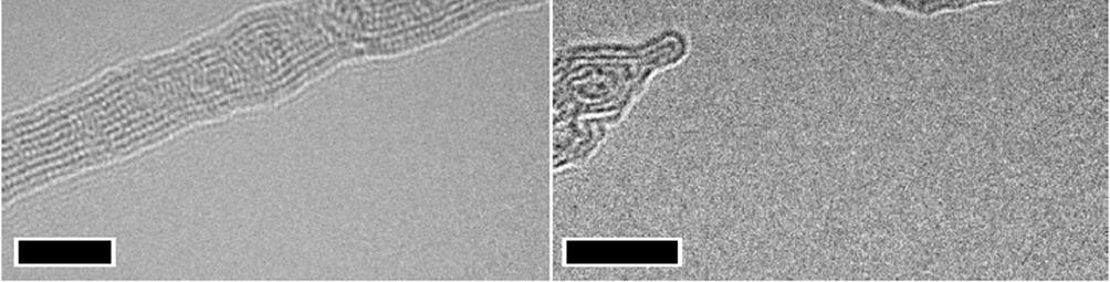
3 graphene sheets on the PMMA surface with an optical microscope, a drop of isopropanol is added to the surface. A SiN x membrane substrate is then placed onto the drop over a region containing graphene sheets, with its surface facing the PMMA surface. As the isopropanol evaporates, its surface tension brings the two surfaces into a close contact, which is further improved by heating at ~ 200 C for ~ 5 minutes. Finally, the PMMA is dissolved in acetone, which releases the graphene sheets on the PMMA side and allows them to transfer and stick to the SiN x membrane substrate. Graphene sheets suspended over a hole in the SiN x membrane were identified in a TEM (JEOL 2010F operating at 200 kv). The number of graphene layers in a sheet could often be determined by imaging the edge of a folded region, 11 in a manner similar to counting the number of tubes in a multi-walled nanotube. We have worked with samples ranging in thickness roughly from 1-20 graphene layers, though the majority of graphene sheets used in this work were composed of ~ 5 layers. Using a method described previously, arbitrary patterns were created in the graphene sheets by increasing the TEM magnification to ~ 800,000x, condensing the imaging electron beam to its minimum diameter, ~ 1 nm, and moving the beam position with the condenser deflectors. 25 To avoid EBID of carbon, likely to occur for a spot-mode beam setting, nanosculpting was performed with the beam at cross-over in a diffusive mode. With the beam at cross-over, the current density measured on the imaging screen was ~ 50 pa/cm 2 which, after accounting for magnification, corresponds to an estimated ~ 0.3 pa/nm 2 at the sample position. The exposure of the graphene sheets to the beam was ~ 1 s/nm 2. All of the structures shown were made at room temperature. Figures 1(a)-(c) show TEM images of a graphene sheet before and after creating a ~ 3.5 nm diameter nanopore by irradiating this spot with the condensed electron beam for ~ 5 s. We have also observed that very brief (~ 500 ms) exposure of graphene sheets to the condensed electron beam can be used to create a partial nanopore by removing a fraction of the graphene layers, while leaving other layers intact. A single nanopore is the 3
4 simplest structure that can be made by ablation, yet nanopores have proven extremely valuable in studies of molecular translocation, DNA in particular. 26 Given that graphene is the thinnest possible membrane yet at the same time structurally robust 9 and impermeable, 27 nanopores in graphene sheets may be useful for achieving significant resolution enhancement in molecular translocation measurements. As shown in Fig. 1(d), multiple nanopores can be made in close proximity to each other, indicating that large arrays of closely packed nanopore arrays can be achieved. Since the average irradiation exposure time per nanopore is on the order of seconds, serial processing is not prohibitively time intensive and large arrays or more complicated geometries can be made quickly. Moreover, parallel fabrication with multiple electron beams would allow for substantial scalability. All of the nanopores that we have made have a concentric ring-like structure extending several nanometers away from their edges. This ring-like structure, evident in Figs. 1(c) and 1(d), bares a close resemblance to the dark lines often observed at the edge of a folded graphene sheet, an example of which is shown in Fig. 1(e). The orientation of a folded graphene layer s edge is locally parallel to the TEM beam and consequently each layer in a folded graphene sheet introduces a dark line along the edge of the fold, 11 similar to what is seen at the radial edges of a multi-walled carbon nanotube. Intensity cross-sections [Figs. 1(f) and 1(g)] obtained from the images of the folded graphene sheet [Fig. 1(c)] and nanopore [Fig. 1(d)] reveal an average spacing between dark lines of nm and nm, respectively. These values are equivalent within the error introduced by finite TEM resolution and are close to the inter-layer distance of HOPG (~ 0.34 nm). These observations suggest that irradiation can induce coordinated inter-layer bonding between freshly exposed layer edges, leading in this case to an inverted-onion - like structure. Irradiation of carbon systems has been previously shown to be capable of inducing a variety of structural changes 28 and our results demonstrate that graphene sheets can provide a valuable initial system for deriving carbon morphologies. 4
5 Figure 2(a) shows two parallel ~ 6 nm wide lines, i.e., regions where graphene has been removed, separated by ~ 25 nm. Starting with these lines, additional focused irradiation was used to gradually increase the lines widths until their separation was reduced to ~ 5 nm, resulting in a nanobridge [Figs. 2(b) and 2(c)]. Although the final nanobridge is highly crystalline [Fig. 2(c)], the extensive exposure to irradiation may have induced significant inter-layer rebonding and atomic restructuring within individual layers. Nanobridges can be cut with the TEM beam to create a gap [Fig. 2(d)] with initial size less than a nanopore diameter but quickly increasing with continued irradiation. In the regions near the cut, irradiation induces morphological changes of the crystalline structure and, in particular, we observe that cut ends close completely, similar to fullerene capping observed for irradiated nanotubes. 28 Such carbon-based point contacts and nanobridges directly connected to a larger graphene structure may find use in mechanical and electrical applications. In conclusion, we have demonstrated that suspended graphene sheets can be controllably nanosculpted with electron-beam irradiation. The ability to introduce features into suspended graphene sheets by electron-beam-induced cutting and reshaping with high spatial resolution expands their value as TEM compatible platforms and offers a route to fabricating graphitic structures for potential use in electrical, mechanical and molecular translocation studies. 5
6 Acknowledgements This work has been partially supported by NSF (NSF Career Award DMR , NSF NSEC DMR and MRSEC DMR ), ONR YIP N , the Penn Genome Frontiers Institute and a grant with the Pennsylvania Department of Health. The Department of Health specifically disclaims responsibility for any analyses, interpretations, or conclusions. 6
7 References [1] Y. Zhang, J. P. Small, W. V. Pontius, and P. Kim, Appl. Phys. Lett. 86, (2005). [2] K. S. Novoselov, D. Jiang, F. Schedin, T. J. Booth, V. V. Khotkevich, S. V. Morozov, and A. K. Geim, PNAS 102, (2005). [3] A. K. Geim and K. S. Novoselov, Nature Mat. 6, 183 (2007). [4] A. H. Castro Neto, F. Guinea, N. M. R. Peres, K. S. Novoselov, and A. K. Geim, cond-mat/ (2007). [5] R. R. Nair, P. Blake, A. N. Grigorenko, K. S. Novoselov, T. J. Booth, T. Stauber, N. M. R. Peres, and A. K. Geim, Science 320, 1308 (2008). [6] N. Tombros, C. Jozsa, M. Popinciuc, H. T. Jonkman, and B. J. van Wees, Nature 448, 571 (2007). [7] K. S. Novoselov, Z. Jiang, Y. Zhang, S. V. Morozov, H. L. Stormer, U. Zeitler, J. C. Maan, G. S. Boebinger, P. Kim, and A. K. Geim, Science 315, 1379 (2008). [8] K. I. Bolotin, K. J. Sikes, Z. Jiang, M. Klima, G. Fudenberg, J. Hone, P. Kim, and H. L. Stormer, Solid State Comm. 146, 351 (2008). [9] C. Lee, X. Wei, J. W., Kysar, and J. Hone, Science 321, 385 (2008). [10] T. J. Booth, P. Blake, R. R. Nair, D. Jiang, E. W. Hill, U. Bangert, A. Bleloch, M. Gass, K. S. Novoselov, M. I. Katsnelson, and A. K. Geim, Nano Lett. asap (2008). [11] J. C. Meyer, A. K. Geim, M. I. Katsnelson, K. S. Novoselov, T. J. Booth and S. Roth, Nature 446, 60 (2007). [12] J. C. Meyer, D. Kisielowski, R. Erni, M. D. Rossell, M. F. Crommie, and A. Zettl, Nano Lett. asap (2008). [13] J. C. Meyer, C. O. Girit, M. F. Crommie, and A. Zettl, Nature 454, 319 (2008). [14] J. C. Meyer, C. O. Girit, M. F. Crommie, and A. Zettl, Appl. Phys. Lett. 92, (2008). 7
8 [15] C. Berger, Z. Song, X. Li, X. Wu, N. Brown, C. Naud, D. Mayou, T. Li, J. Hass, A. N. Marchenkov, E. H. Conrad, P. N. First, and W. A. de Heer, Science 3012, 1191 (2006). [16] J. S. Bunch, Y. Yaish, M. Brink, K. Bolotin, and P. L. McEuen, Nano Lett. 5, 287 (2005). [17] L. A. Ponomarenko, F. Schedin, M. I. Katsnelson, R. Yang, E. W. Hill, K. S. Novoselov, and A. K. Geim, Science 320, 356 (2008). [18] M. Y. Han, B. Ozylmaz, Y. Zhang, and P. Kim, Phys. Rev. Lett. 98, (2007). [19] C. Stampfer, J. Guttinger, F. Molitor, D. Graf, T. Ihn, and K. Ensslin, Appl. Phys. Lett. 92, (2008). [20] Z. Chen, Y.-M. Lin, M. J. Rooks, and P. Avouris, Physica E 40, 228 (2007). [21] X. Li, X. Wang, L. Zhang, S. Lee, and H. Dai, Science 319, (2008). [22] S. S. Datta, D. R. Strachan, S. M. Khamis, and A. T. Johnson, Nano Lett. 8, 1912 (2008). [23] L. Tapaszto, G. Dobrik, P. Lambin, and L. P. Biro, Nature Nanotech. 3, 397 (2008). [24] M. D. Fischbein and M. Drndic, Appl. Phys. Lett. 88 (6), (2006). [25] M. D. Fischbein and M. Drndic, Nano Lett. 7, 1329 (2007). [26] K. Healy, B. Schiedt, and A.P. Morrison, Nanomedicine 2, 875 (2007). [27] J. S. Bunch, S. S. Verbridge, J. S. Alden, A. M. van der Zande, J. M. Parpia, H.G. Craighead, and P. L. McEuen, Nano Lett. asap (2008). [28] For review see, A. V. Krasheninnikov and F. Banhart, Nature Mater. 6, 723 (2007) and references therein. 8
9 Figure Captions Figure 1 TEM images of a suspended graphene sheet is shown (a) before and (b) after a nanopore is made by electron beam ablation. (c) Higher magnification image of the nanopore. (d) Multiple nanopores made in close proximity to each other. (e) Folded edge of a graphene sheet showing lines corresponding to layer number. These lines are similar to those seen around the nanopores (Scale bars are 50, 50, 2, 10, 5 nm). (f) Average of intensity crosssections taken along 6 different radial directions of the nanopore in (c), each starting at the edge and proceeding radially outward. (g) Average of 6 intensity cross-sections of the graphene sheet in (e), each taken perpendicular to and starting at the sheet edge. Figure 2 (a) Two ~ 6 nm lines cut into a graphene sheet. (b) Electron irradiation is continued to create a ~ 5 nm wide bridge. (c) Higher resolution of the bridge shows clear atomic order. (d) Small gap opened in the nanobridge by additional electron irradiation. We note that the cut ends are closed. (Scale bars are 20, 10, 5, 5 nm). 9


10 Figure 1 10


11 Figure 2 11
Graphene Thickness Determination Using Reflection and Contrast Spectroscopy
 Graphene Thickness Determination Using Reflection and Contrast Spectroscopy NANO LETTERS 2007 Vol. 7, No. 9 2758-2763 Z. H. Ni, H. M. Wang, J. Kasim, H. M. Fan,, T. Yu, Y. H. Wu, Y. P. Feng, and Z. X.
Edge chirality determination of graphene by Raman spectroscopy
 Edge chirality determination of graphene by Raman spectroscopy YuMeng You, ZhenHua Ni, Ting Yu, ZeXiang Shen a) Division of Physics and Applied Physics, School of Physical and Mathematical Sciences, Nanyang
Ambipolar Graphene Field Effect Transistors by Local Metal Side Gates USA. Indiana 47907, USA. Abstract
 Ambipolar Graphene Field Effect Transistors by Local Metal Side Gates J. F. Tian *, a, b, L. A. Jauregui c, b, G. Lopez c, b, H. Cao a, b *, a, b, c, and Y. P. Chen a Department of Physics, Purdue University,
Etching of Graphene Devices with a Helium Ion Beam
 Etching of Graphene Devices with a Helium Ion Beam The Harvard community has made this article openly available. Please share how this access benefits you. Your story matters Citation Lemme, Max C., David
Precision Cutting and Patterning of Graphene with Helium Ions. 1.School of Engineering and Applied Sciences, Harvard University, Cambridge MA 02138
 Precision Cutting and Patterning of Graphene with Helium Ions D.C. Bell 1,2, M.C. Lemme 3, L. A. Stern 4, J.R. Williams 1,3, C. M. Marcus 3 1.School of Engineering and Applied Sciences, Harvard University,
Effect of electron-beam irradiation on graphene field effect devices
 Effect of electron-beam irradiation on graphene field effect devices Isaac Childres 1,2, Luis A. Jauregui 2,3, Mike Foxe 4,#, Jifa Tian 1,2, Romaneh Jalilian 1,2,*, Igor Jovanovic 4,#, Yong P. Chen 1,2,3,$
From One Electron to One Hole: Quasiparticle Counting in Graphene Quantum Dots Determined by Electrochemical and Plasma Etching
 From One Electron to One Hole: Quasiparticle Counting in Graphene Quantum Dots Determined by Electrochemical and Plasma Etching S. Neubeck 1, L. A. Ponomarenko 1, F. Freitag 1, A. J. M. Giesbers 2, U.
Lithography-free Fabrication of High Quality Substrate-supported and. Freestanding Graphene devices
 Lithography-free Fabrication of High Quality Substrate-supported and Freestanding Graphene devices W. Bao 1, G. Liu 1, Z. Zhao 1, H. Zhang 1, D. Yan 2, A. Deshpande 3, B.J. LeRoy 3 and C.N. Lau 1, * 1
Multilayer graphene under vertical electric field
 Multilayer graphene under vertical electric field S. Bala kumar and Jing Guo a) Department of Electrical and Computer Engineering, University of Florida, Gainesville, Florida 3608, USA Abstract We study
ICTP Conference Graphene Week 2008
 1960-3 ICTP Conference Graphene Week 2008 25-29 August 2008 Current-induced cleaning of graphene J. Moser CIN2 Barcelona, Campus UAB, Bellaterra, Spain A. Barreiro CIN2 Barcelona, Campus UAB, Bellaterra,
Determination of the Number of Graphene Layers: Discrete. Distribution of the Secondary Electron Intensity Derived from
 Determination of the Number of Graphene Layers: Discrete Distribution of the Secondary Electron Intensity Derived from Individual Graphene Layers Hidefumi Hiura 1, 2 *, Hisao Miyazaki 2, 3, and Kazuhito
TRANSVERSE SPIN TRANSPORT IN GRAPHENE
 International Journal of Modern Physics B Vol. 23, Nos. 12 & 13 (2009) 2641 2646 World Scientific Publishing Company TRANSVERSE SPIN TRANSPORT IN GRAPHENE TARIQ M. G. MOHIUDDIN, A. A. ZHUKOV, D. C. ELIAS,
Raman spectroscopy of graphene on different substrates and influence of defects
 Bull. Mater. Sci., Vol. 31, No. 3, June 2008, pp. 579 584. Indian Academy of Sciences. Raman spectroscopy of graphene on different substrates and influence of defects ANINDYA DAS, BISWANATH CHAKRABORTY
Raman Imaging and Electronic Properties of Graphene
 Raman Imaging and Electronic Properties of Graphene F. Molitor, D. Graf, C. Stampfer, T. Ihn, and K. Ensslin Laboratory for Solid State Physics, ETH Zurich, 8093 Zurich, Switzerland ensslin@phys.ethz.ch
The role of charge traps in inducing hysteresis: capacitance voltage measurements on top gated bilayer graphene
 The role of charge traps in inducing hysteresis: capacitance voltage measurements on top gated bilayer graphene Gopinadhan Kalon, Young Jun Shin, Viet Giang Truong, Alan Kalitsov, and Hyunsoo Yang a) Department
In-situ electronic characterization of graphene nanoconstrictions fabricated in a transmission electron microscope
 In-situ electronic characterization of graphene nanoconstrictions fabricated in a transmission electron microscope Ye Lu, Christopher A. Merchant, Marija Drndić, A. T. Charlie Johnson Department of Physics
Quantum transport through graphene nanostructures
 Quantum transport through graphene nanostructures S. Rotter, F. Libisch, L. Wirtz, C. Stampfer, F. Aigner, I. Březinová, and J. Burgdörfer Institute for Theoretical Physics/E136 December 9, 2009 Graphene
Polarization dependence of photocurrent in a metalgraphene-metal
 Polarization dependence of photocurrent in a metalgraphene-metal device Minjung Kim, 1 Ho Ang Yoon, 2 Seungwoo Woo, 1 Duhee Yoon, 1 Sang Wook Lee, 2 and Hyeonsik Cheong 1,a) 1 Department of Physics, Sogang
G raphene1,2 is a unique material that may soon find use in
 pubs.acs.org/nanolett In Situ Electronic Characterization of Graphene Nanoconstrictions Fabricated in a Transmission Electron Microscope Ye Lu, Christopher A. Merchant, Marija Drndic,* and A. T. Charlie
Scanning Tunneling Microscopy Characterization of the Electrical Properties of Wrinkles in Exfoliated Graphene Monolayers
 Scanning Tunneling Microscopy Characterization of the Electrical Properties of Wrinkles in Exfoliated Graphene Monolayers NANO LETTERS 2009 Vol. 9, No. 12 4446-4451 Ke Xu, Peigen Cao, and James R. Heath*
Raman spectroscopy study of rotated double-layer graphene: misorientation angle dependence of electronic structure
 Supplementary Material for Raman spectroscopy study of rotated double-layer graphene: misorientation angle dependence of electronic structure Kwanpyo Kim 1,2,3, Sinisa Coh 1,3, Liang Z. Tan 1,3, William
Sub-5 nm Patterning and Applications by Nanoimprint Lithography and Helium Ion Beam Lithography
 Sub-5 nm Patterning and Applications by Nanoimprint Lithography and Helium Ion Beam Lithography Yuanrui Li 1, Ahmed Abbas 1, Yuhan Yao 1, Yifei Wang 1, Wen-Di Li 2, Chongwu Zhou 1 and Wei Wu 1* 1 Department
Lithography-Free Fabrication of High Quality Substrate- Supported and Freestanding Graphene Devices
 98 DOI 10.1007/s12274-010-1013-5 Research Article Lithography-Free Fabrication of High Quality Substrate- Supported and Freestanding Graphene Devices Wenzhong Bao 1, Gang Liu 1, Zeng Zhao 1, Hang Zhang
Reduction of Fermi velocity in folded graphene observed by resonance Raman spectroscopy
 Reduction of Fermi velocity in folded graphene observed by resonance Raman spectroscopy Zhenhua Ni, Yingying Wang, Ting Yu, Yumeng You, and Zexiang Shen* Division of Physics and Applied Physics, School
Supporting Online Material for
 www.sciencemag.org/cgi/content/full/320/5874/356/dc1 Supporting Online Material for Chaotic Dirac Billiard in Graphene Quantum Dots L. A. Ponomarenko, F. Schedin, M. I. Katsnelson, R. Yang, E. W. Hill,
High-Quality BN-Graphene-BN Nanoribbon Capacitors Modulated by Graphene Side-gate Electrodes
 High-Quality BN-Graphene-BN Nanoribbon Capacitors Modulated by Graphene Side-gate Electrodes Yang Wang, Xiaolong Chen, Weiguang Ye, Zefei Wu, Yu Han, Tianyi Han, Yuheng He, Yuan Cai and Ning Wang* Department
Quantum Hall effect in graphene
 Solid State Communications 143 (2007) 14 19 www.elsevier.com/locate/ssc Quantum Hall effect in graphene Z. Jiang a,b, Y. Zhang a, Y.-W. Tan a, H.L. Stormer a,c, P. Kim a, a Department of Physics, Columbia
Correlation between structure and electrical transport in ion-irradiated graphene grown on Cu foils CA 94720;
 1 Correlation between structure and electrical transport in ion-irradiated graphene grown on Cu foils Grant Buchowicz 1,2, Peter R. Stone 1,2, Jeremy T. Robinson 3, Cory D. Cress 3, Jeffrey W. Beeman 1,
Supporting Information. by Hexagonal Boron Nitride
 Supporting Information High Velocity Saturation in Graphene Encapsulated by Hexagonal Boron Nitride Megan A. Yamoah 1,2,, Wenmin Yang 1,3, Eric Pop 4,5,6, David Goldhaber-Gordon 1 * 1 Department of Physics,
performance electrocatalytic or electrochemical devices. Nanocrystals grown on graphene could have
 Nanocrystal Growth on Graphene with Various Degrees of Oxidation Hailiang Wang, Joshua Tucker Robinson, Georgi Diankov, and Hongjie Dai * Department of Chemistry and Laboratory for Advanced Materials,
Supplementary Information for
 Supplementary Information for Highly Stable, Dual-Gated MoS 2 Transistors Encapsulated by Hexagonal Boron Nitride with Gate-Controllable Contact Resistance and Threshold Voltage Gwan-Hyoung Lee, Xu Cui,
Ambipolar bistable switching effect of graphene
 Ambipolar bistable switching effect of graphene Young Jun Shin, 1,2 Jae Hyun Kwon, 1,2 Gopinadhan Kalon, 1,2 Kai-Tak Lam, 1 Charanjit S. Bhatia, 1 Gengchiau Liang, 1 and Hyunsoo Yang 1,2,a) 1 Department
Molecular Dynamics Study of Thermal Rectification in Graphene Nanoribbons
 Molecular Dynamics Study of Thermal Rectification in Graphene Nanoribbons Jiuning Hu 1* Xiulin Ruan 2 Yong P. Chen 3# 1School of Electrical and Computer Engineering and Birck Nanotechnology Center, Purdue
Intrinsic Electronic Transport Properties of High. Information
 Intrinsic Electronic Transport Properties of High Quality and MoS 2 : Supporting Information Britton W. H. Baugher, Hugh O. H. Churchill, Yafang Yang, and Pablo Jarillo-Herrero Department of Physics, Massachusetts
Hybrid Surface-Phonon-Plasmon Polariton Modes in Graphene /
 Supplementary Information: Hybrid Surface-Phonon-Plasmon Polariton Modes in Graphene / Monolayer h-bn stacks Victor W. Brar 1,2, Min Seok Jang 3,, Michelle Sherrott 1, Seyoon Kim 1, Josue J. Lopez 1, Laura
Quantum transport through graphene nanostructures
 Quantum transport through graphene nanostructures F. Libisch, S. Rotter, and J. Burgdörfer Institute for Theoretical Physics/E136, January 14, 2011 Graphene [1, 2], the rst true two-dimensional (2D) solid,
Thickness Estimation of Epitaxial Graphene on SiC using Attenuation of Substrate Raman Intensity
 Thickness Estimation of Epitaxial Graphene on SiC using Attenuation of Substrate Raman Intensity Shriram Shivaraman 1, MVS Chandrashekhar 1, John J. Boeckl 2, Michael G. Spencer 1 1 School of Electrical
Graphene as a transparent conductive support for studying biological molecules by transmission electron microscopy
 Graphene as a transparent conductive support for studying biological molecules by transmission electron microscopy R. R. Nair 1, P. Blake 2, J. R. Blake 2, R. Zan 1,3, S. Anissimova 1, U. Bangert 3, A.
Fabrication of graphene nanogap with crystallographically matching edges and its. electron emission properties
 Fabrication of graphene nanogap with crystallographically matching edges and its electron emission properties H. M. Wang, 1 Z. Zheng, 1 Y.Y.Wang, 1 J.J. Qiu, Z.B. Guo, Z. X. Shen, 1 and T. Yu 1,* 1 Division
Supporting Information. Direct Growth of Graphene Films on 3D Grating. Structural Quartz Substrates for High-performance. Pressure-Sensitive Sensor
 Supporting Information Direct Growth of Graphene Films on 3D Grating Structural Quartz Substrates for High-performance Pressure-Sensitive Sensor Xuefen Song, a,b Tai Sun b Jun Yang, b Leyong Yu, b Dacheng
arxiv:cond-mat/ v1 [cond-mat.mtrl-sci] 12 Jun 2006
![arxiv:cond-mat/ v1 [cond-mat.mtrl-sci] 12 Jun 2006](/thumbs/74/71073497.jpg "arxiv:cond-mat/ v1 [cond-mat.mtrl-sci] 12 Jun 2006") The Raman Fingerprint of Graphene arxiv:cond-mat/66284v1 [cond-mat.mtrl-sci] 12 Jun 26 A. C. Ferrari 1, J. C. Meyer 2, V. Scardaci 1, C. Casiraghi 1, M. Lazzeri 2, F. Mauri 2, S. Piscanec 1, Da Jiang 4,
The Raman Fingerprint of Graphene arxiv:cond-mat/66284v1 [cond-mat.mtrl-sci] 12 Jun 26 A. C. Ferrari 1, J. C. Meyer 2, V. Scardaci 1, C. Casiraghi 1, M. Lazzeri 2, F. Mauri 2, S. Piscanec 1, Da Jiang 4,
Research Article Graphene and Other 2D Material Components Dynamic Characterization and Nanofabrication at Atomic Scale
 Nanomaterials Volume 2015, Article ID 198126, 6 pages http://dx.doi.org/10.1155/2015/198126 Research Article Graphene and Other 2D Material Components Dynamic Characterization and Nanofabrication at Atomic
Efficient Preparation of Large-Area Graphene Oxide Sheets for Transparent Conductive Films
 Supporting Information Efficient Preparation of Large-Area Graphene Oxide Sheets for Transparent Conductive Films Jinping Zhao, Songfeng Pei, Wencai Ren*, Libo Gao and Hui-Ming Cheng* Shenyang National
Perfect spin-fillter and spin-valve in carbon atomic chains
 Perfect spin-fillter and spin-valve in carbon atomic chains M. G. Zeng,1, 2 L. Shen,1 Y. Q. Cai,1 Z. D. Sha,1 and Y. P. Feng1, * 1Department of Physics, National University of Singapore, 2 Science Drive
arxiv: v1 [cond-mat.mtrl-sci] 29 Jan 2008
![arxiv: v1 [cond-mat.mtrl-sci] 29 Jan 2008](/thumbs/85/92280048.jpg "arxiv: v1 [cond-mat.mtrl-sci] 29 Jan 2008") Strong Suppression of Electrical Noise in Bilayer Graphene Nano Devices YU-MING LIN and PHAEDON AVOURIS IBM T. J. Watson Research Center, arxiv:0801.4576v1 [cond-mat.mtrl-sci] 29 Jan 2008 Yorktown Heights,
Strong Suppression of Electrical Noise in Bilayer Graphene Nano Devices YU-MING LIN and PHAEDON AVOURIS IBM T. J. Watson Research Center, arxiv:0801.4576v1 [cond-mat.mtrl-sci] 29 Jan 2008 Yorktown Heights,
Direct Observation of Inner and Outer G Band Double-resonance Raman Scattering in Free Standing Graphene
 Direct Observation of Inner and Outer G Band Double-resonance Raman Scattering in Free Standing Graphene Zhiqiang Luo 1, Chunxiao Cong 1, Jun Zhang 1, Qihua Xiong 1 1, 2, 3*, Ting Yu 1. Division of Physics
Intrinsic Response of Graphene Vapor Sensors
 Intrinsic Response of Graphene Vapor Sensors Yaping Dan, Ye Lu, Nicholas J. Kybert, A. T. Charlie Johnson Department of Electrical and Systems Engineering, University of Pennsylvania, Philadelphia, PA
AN IMPROVED METHOD FOR TRANSFERRING GRAPHENE GROWN BY CHEMICAL VAPOR DEPOSITION
 NANO: Brief Reports and Reviews Vol. 7, No. 1 (2012) 1150001 (6 pages) World Scienti c Publishing Company DOI: 10.1142/S1793292011500019 AN IMPROVED METHOD FOR TRANSFERRING GRAPHENE GROWN BY CHEMICAL VAPOR
Supporting Information Available:
 Supporting Information Available: Photoresponsive and Gas Sensing Field-Effect Transistors based on Multilayer WS 2 Nanoflakes Nengjie Huo 1, Shengxue Yang 1, Zhongming Wei 2, Shu-Shen Li 1, Jian-Bai Xia
Impact of Calcium on Transport Property of Graphene. Jyoti Katoch and Masa Ishigami*
 Impact of Calcium on Transport Property of Graphene Jyoti Katoch and Masa Ishigami* Department of Physics and Nanoscience Technology Center, University of Central Florida, Orlando, FL, 32816 *Corresponding
Despite the intense interest in the measurements and
 pubs.acs.org/nanolett Direct Measurement of Adhesion Energy of Monolayer Graphene As- Grown on Copper and Its Application to Renewable Transfer Process Taeshik Yoon,, Woo Cheol Shin,, Taek Yong Kim, Jeong
Optimizing Graphene Morphology on SiC(0001)
") Optimizing Graphene Morphology on SiC(0001) James B. Hannon Rudolf M. Tromp Graphene sheets Graphene sheets can be formed into 0D,1D, 2D, and 3D structures Chemically inert Intrinsically high carrier mobility
Optimizing Graphene Morphology on SiC(0001) James B. Hannon Rudolf M. Tromp Graphene sheets Graphene sheets can be formed into 0D,1D, 2D, and 3D structures Chemically inert Intrinsically high carrier mobility
Scanning tunneling microscopy and spectroscopy of graphene layers on graphite
 Scanning tunneling microscopy and spectroscopy of graphene layers on graphite Adina Luican, Guohong Li and Eva Y. Andrei Department of Physics and Astronomy, Rutgers University, Piscataway, New Jersey
SUPPLEMENTARY INFORMATION
 SUPPLEMENTARY INFORMATION Facile Synthesis of High Quality Graphene Nanoribbons Liying Jiao, Xinran Wang, Georgi Diankov, Hailiang Wang & Hongjie Dai* Supplementary Information 1. Photograph of graphene
Graphene Segregated on Ni surfaces and Transferred to Insulators
 Graphene Segregated on Ni surfaces and Transferred to Insulators Qingkai Yu Center for Advanced Materials, Electrical and Computer Engineering, University of Houston, Houston, Texas 77204 Jie Lian Department
Tunable Graphene Single Electron Transistor
 Tunable Graphene Single Electron Transistor NANO LETTERS 2008 Vol. 8, No. 8 2378-2383 C. Stampfer,* E. Schurtenberger, F. Molitor, J. Güttinger, T. Ihn, and K. Ensslin Solid State Physics Laboratory, ETH
Supplementary Figure 1 Detailed illustration on the fabrication process of templatestripped
 Supplementary Figure 1 Detailed illustration on the fabrication process of templatestripped gold substrate. (a) Spin coating of hydrogen silsesquioxane (HSQ) resist onto the silicon substrate with a thickness
MECHANICAL PROPERTIES OF GRAPHENE NANORIBBONS: A SELECTIVE REVIEW OF COMPUTER SIMULATIONS
 Mechanical Rev. Adv. Mater. properties Sci. 40 of (2015) graphene 249-256 nanoribbons: a selective review of computer simulations 249 MECHANICAL PROPERTIES OF GRAPHENE NANORIBBONS: A SELECTIVE REVIEW OF
arxiv: v3 [cond-mat.mtrl-sci] 16 Aug 2008
![arxiv: v3 [cond-mat.mtrl-sci] 16 Aug 2008](/thumbs/86/93290957.jpg "arxiv: v3 [cond-mat.mtrl-sci] 16 Aug 2008") Measurement of the Optical Absorption Spectra of Epitaxial Graphene from Terahertz to Visible Jahan M. Dawlaty, Shriram Shivaraman, Jared Strait, Paul George, Mvs Chandrashekhar, Farhan Rana, and Michael
Measurement of the Optical Absorption Spectra of Epitaxial Graphene from Terahertz to Visible Jahan M. Dawlaty, Shriram Shivaraman, Jared Strait, Paul George, Mvs Chandrashekhar, Farhan Rana, and Michael
Multicolor Graphene Nanoribbon/Semiconductor Nanowire. Heterojunction Light-Emitting Diodes
 Multicolor Graphene Nanoribbon/Semiconductor Nanowire Heterojunction Light-Emitting Diodes Yu Ye, Lin Gan, Lun Dai, *, Hu Meng, Feng Wei, Yu Dai, Zujin Shi, Bin Yu, Xuefeng Guo, and Guogang Qin *, State
status solidi Department of Physics, University of California at Berkeley, Berkeley, CA, USA 2
 physica pss status solidi basic solid state physics b Extreme thermal stability of carbon nanotubes G. E. Begtrup,, K. G. Ray, 3, B. M. Kessler, T. D. Yuzvinsky,, 3, H. Garcia,,, 3 and A. Zettl Department
Supporting Information
 Supporting Information Thickness of suspended epitaxial graphene (SEG) resonators: Graphene thickness was estimated using an atomic force microscope (AFM) by going over the step edge from SiC to graphene.
Supplementary information
 Supplementary information Electrochemical synthesis of metal and semimetal nanotube-nanowire heterojunctions and their electronic transport properties Dachi Yang, ab Guowen Meng,* a Shuyuan Zhang, c Yufeng
Graphene devices and integration: A primer on challenges
 Graphene devices and integration: A primer on challenges Archana Venugopal (TI) 8 Nov 2016 Acknowledgments: Luigi Colombo (TI) UT Dallas and UT Austin 1 Outline Where we are Issues o Contact resistance
Epitaxial graphene on SiC formed by the surface structure control technique
 Epitaxial graphene on SiC formed by the surface structure control technique Takuya Aritsuki*, Takeshi Nakashima, Keisuke Kobayashi, Yasuhide Ohno, and Masao Nagase Tokushima University, Tokushima 770-8506,
arxiv: v1 [cond-mat.mes-hall] 22 Dec 2011
![arxiv: v1 [cond-mat.mes-hall] 22 Dec 2011](/thumbs/76/73542175.jpg "arxiv: v1 [cond-mat.mes-hall] 22 Dec 2011") Direct Measurement of the Fermi Energy in Graphene Using a Double Layer Structure Seyoung Kim, 1 Insun Jo, 2 D. C. Dillen, 1 D. A. Ferrer, 1 B. Fallahazad, 1 Z. Yao, 2 S. K. Banerjee, 1 and E. Tutuc 1
Direct Measurement of the Fermi Energy in Graphene Using a Double Layer Structure Seyoung Kim, 1 Insun Jo, 2 D. C. Dillen, 1 D. A. Ferrer, 1 B. Fallahazad, 1 Z. Yao, 2 S. K. Banerjee, 1 and E. Tutuc 1
Application Note. Graphene Characterization by Correlation of Scanning Electron, Atomic Force and Interference Contrast Microscopy
 Graphene Characterization by Correlation of Scanning Electron, Atomic Force and Interference Contrast Microscopy Graphene Characterization by Correlation of Scanning Electron, Atomic Force and Interference
Supporting Information. Fast Synthesis of High-Performance Graphene by Rapid Thermal Chemical Vapor Deposition
 1 Supporting Information Fast Synthesis of High-Performance Graphene by Rapid Thermal Chemical Vapor Deposition Jaechul Ryu, 1,2, Youngsoo Kim, 4, Dongkwan Won, 1 Nayoung Kim, 1 Jin Sung Park, 1 Eun-Kyu
Supplementary Figure 1. Selected area electron diffraction (SAED) of bilayer graphene and tblg. (a) AB
 of bilayer graphene and tblg. (a) AB") Supplementary Figure 1. Selected area electron diffraction (SAED) of bilayer graphene and tblg. (a) AB stacked bilayer graphene (b), (c), (d), (e), and (f) are twisted bilayer graphene with twist angle
Supplementary Figure 1. Selected area electron diffraction (SAED) of bilayer graphene and tblg. (a) AB stacked bilayer graphene (b), (c), (d), (e), and (f) are twisted bilayer graphene with twist angle
state spectroscopy Xing Lan Liu, Dorothee Hug, Lieven M. K. Vandersypen Netherlands
 Gate-defined graphene double quantum dot and excited state spectroscopy Xing Lan Liu, Dorothee Hug, Lieven M. K. Vandersypen Kavli Institute of Nanoscience, Delft University of Technology, P.O. Box 5046,
Molecular Dynamics Study of Thermal Rectification in Graphene Nanoribbons
 Int J Thermophys (2012) 33:986 991 DOI 10.1007/s10765-012-1216-y Molecular Dynamics Study of Thermal Rectification in Graphene Nanoribbons Jiuning Hu Xiulin Ruan Yong P. Chen Received: 26 June 2009 / Accepted:
arxiv: v1 [cond-mat.mes-hall] 29 Nov 2013
![arxiv: v1 [cond-mat.mes-hall] 29 Nov 2013](/thumbs/74/71156913.jpg "arxiv: v1 [cond-mat.mes-hall] 29 Nov 2013") Transport Spectroscopy of a Graphene Quantum Dot Fabricated by Atomic Force Microscope Nanolithography R.K. Puddy, 1 C.J. Chua, 1 1,2, 3, and M.R. Buitelaar 1 Cavendish Laboratory, University of Cambridge,
Transport Spectroscopy of a Graphene Quantum Dot Fabricated by Atomic Force Microscope Nanolithography R.K. Puddy, 1 C.J. Chua, 1 1,2, 3, and M.R. Buitelaar 1 Cavendish Laboratory, University of Cambridge,
Initial Stages of Growth of Organic Semiconductors on Graphene
 Initial Stages of Growth of Organic Semiconductors on Graphene Presented by: Manisha Chhikara Supervisor: Prof. Dr. Gvido Bratina University of Nova Gorica Outline Introduction to Graphene Fabrication
Spatially resolved spectroscopy of monolayer graphene on SiO 2
 Spatially resolved spectroscopy of monolayer graphene on SiO 2 A. Deshpande, 1 W. Bao, 2 F. Miao, 2 C. N. Lau, 2 and B. J. LeRoy 1, * 1 Department of Physics, University of Arizona, Tucson, Arizona 85721,
A BIT OF MATERIALS SCIENCE THEN PHYSICS
 GRAPHENE AND OTHER D ATOMIC CRYSTALS Andre Geim with many thanks to K. Novoselov, S. Morozov, D. Jiang, F. Schedin, I. Grigorieva, J. Meyer, M. Katsnelson A BIT OF MATERIALS SCIENCE THEN PHYSICS CARBON
Thermal Transport in Suspended and Supported Monolayer Graphene Grown by Chemical Vapor Deposition
 Thermal Transport in Suspended and Supported Monolayer Graphene Grown by Chemical Vapor Deposition Weiwei Cai, Arden L. Moore, Yanwu Zhu, Xuesong Li, Shanshan Chen, Li Shi,* and Rodney S. Ruoff* pubs.acs.org/nanolett
Wafer-Scale Single-Domain-Like Graphene by. Defect-Selective Atomic Layer Deposition of
 Electronic Supplementary Material (ESI) for Nanoscale. This journal is The Royal Society of Chemistry 2015 Wafer-Scale Single-Domain-Like Graphene by Defect-Selective Atomic Layer Deposition of Hexagonal
A Chemical Route to Graphene for Device Applications
 A Chemical Route to Graphene for Device Applications NANO LETTERS xxxx Vol. 0, No. 0 A-E Scott Gilje, Song Han, Minsheng Wang, Kang L. Wang, and Richard B. Kaner*, Department of Chemistry and Biochemistry
Towards electron transport measurements in chemically modified graphene: effect of a solvent
 Towards electron transport measurements in chemically modified graphene: effect of a solvent To cite this article: Arnhild Jacobsen et al 2010 New J. Phys. 12 125007 View the article online for updates
Graphene Segregated on Ni surfaces and Transferred to Insulators
 Graphene Segregated on Ni surfaces and Transferred to Insulators Qingkai Yu Center for Advanced Materials, Electrical and Computer Engineering, University of Houston, Houston, Texas 77204 Jie Lian Department
Solvothermal Reduction of Chemically Exfoliated Graphene Sheets
 Solvothermal Reduction of Chemically Exfoliated Graphene Sheets Hailiang Wang, Joshua Tucker Robinson, Xiaolin Li, and Hongjie Dai* Department of Chemistry and Laboratory for Advanced Materials, Stanford
Soft Carrier Multiplication by Hot Electrons in Graphene
 Soft Carrier Multiplication by Hot Electrons in Graphene Anuj Girdhar 1,3 and J.P. Leburton 1,2,3 1) Department of Physics 2) Department of Electrical and Computer Engineering, and 3) Beckman Institute
Raman spectroscopy at the edges of multilayer graphene
 Raman spectroscopy at the edges of multilayer graphene Q. -Q. Li, X. Zhang, W. -P. Han, Y. Lu, W. Shi, J. -B. Wu, P. -H. Tan* State Key Laboratory of Superlattices and Microstructures, Institute of Semiconductors,
Electronic Doping and Scattering by Transition Metals on Graphene
 Electronic Doping and Scattering by Transition Metals on Graphene K. Pi,* K. M. McCreary,* W. Bao, Wei Han, Y. F. Chiang, Yan Li, S.-W. Tsai, C. N. Lau, and R. K. Kawakami Department of Physics and Astronomy,
Layer-dependent morphologies of silver on n-layer graphene
 Huang et al. Nanoscale Research Letters 2012, 7:618 NANO EXPRESS Layer-dependent morphologies of silver on n-layer graphene Cheng-wen Huang 1, Hsing-Ying Lin 2, Chen-Han Huang 2, Ren-Jye Shiue 3, Wei-Hua
Overview. Carbon in all its forms. Background & Discovery Fabrication. Important properties. Summary & References. Overview of current research
 Graphene Prepared for Solid State Physics II Pr Dagotto Spring 2009 Laurene Tetard 03/23/09 Overview Carbon in all its forms Background & Discovery Fabrication Important properties Overview of current
Supporting Information
 Electronic Supplementary Material (ESI) for Nanoscale. This journal is The Royal Society of Chemistry 2016 Supporting Information Graphene transfer method 1 : Monolayer graphene was pre-deposited on both
Transport Properties of Graphene Nanoribbon Transistors on. Chemical-Vapor-Deposition Grown Wafer-Scale Graphene
 Transport Properties of Graphene Nanoribbon Transistors on Chemical-Vapor-Deposition Grown Wafer-Scale Graphene Wan Sik Hwang 1, a), Kristof Tahy 1, Xuesong Li 2, Huili (Grace) Xing 1, Alan C. Seabaugh
Supplementary Figure 1 Experimental setup for crystal growth. Schematic drawing of the experimental setup for C 8 -BTBT crystal growth.
 Supplementary Figure 1 Experimental setup for crystal growth. Schematic drawing of the experimental setup for C 8 -BTBT crystal growth. Supplementary Figure 2 AFM study of the C 8 -BTBT crystal growth
Controllable Atomic Scale Patterning of Freestanding Monolayer. Graphene at Elevated Temperature
 Controllable Atomic Scale Patterning of Freestanding Monolayer Graphene at Elevated Temperature AUTHOR NAMES Qiang Xu 1, Meng-Yue Wu 1, Grégory F. Schneider 1, Lothar Houben 2, Sairam K. Malladi 1, Cees
SUPPLEMENTARY INFORMATION
 Imaging and Dynamics of Light Atoms and Molecules on Graphene Supplementary information Jannik C. Meyer, Caglar. O. Girit, Michael F. Crommie and Alex Zettl Department of Physics, University of California
Probing the mechanical properties of graphene using a corrugated elastic substrate
 Probing the mechanical properties of graphene using a corrugated elastic substrate Scott Scharfenberg, 1 D. Z. Rocklin, 1, 2 Cesar Chialvo, 1 Richard L. Weaver, 1, 2 Paul M. Goldbart, 1, 2 and Nadya Mason
Large Scale Direct Synthesis of Graphene on Sapphire and Transfer-free Device Fabrication
 Supplementary Information Large Scale Direct Synthesis of Graphene on Sapphire and Transfer-free Device Fabrication Hyun Jae Song a, Minhyeok Son a, Chibeom Park a, Hyunseob Lim a, Mark P. Levendorf b,
Spin Injection into a Graphene Thin Film at Room Temperature
 Spin Injection into a Graphene Thin Film at Room Temperature Megumi Ohishi, Masashi Shiraishi*, Ryo Nouchi, Takayuki Nozaki, Teruya Shinjo, and Yoshishige Suzuki Graduate School of Engineering Science,
Low-temperature ballistic transport in nanoscale epitaxial graphene cross junctions
 Low-temperature ballistic transport in nanoscale epitaxial graphene cross junctions S. Weingart, C. Bock, and U. Kunze Werkstoffe und Nanoelektronik, Ruhr-Universität Bochum, D-44780 Bochum, Germany F.
Supplementary materials for: Large scale arrays of single layer graphene resonators
 Supplementary materials for: Large scale arrays of single layer graphene resonators Arend M. van der Zande* 1, Robert A. Barton 2, Jonathan S. Alden 2, Carlos S. Ruiz-Vargas 2, William S. Whitney 1, Phi
Supplementary Information. Experimental Evidence of Exciton Capture by Mid-Gap Defects in CVD. Grown Monolayer MoSe2
 Supplementary Information Experimental Evidence of Exciton Capture by Mid-Gap Defects in CVD Grown Monolayer MoSe2 Ke Chen 1, Rudresh Ghosh 2,3, Xianghai Meng 1, Anupam Roy 2,3, Joon-Seok Kim 2,3, Feng
Free-Standing Epitaxial Graphene
 Free-Standing Epitaxial Graphene Shriram Shivaraman,* Robert A. Barton, Xun Yu, Jonathan Alden, Lihong Herman, MVS Chandrashekhar, Jiwoong Park, Paul L. McEuen, Jeevak M. Parpia, Harold G. Craighead, and
Stacking-Dependent Optical Conductivity of Bilayer Graphene
 Georgia Southern University Digital Commons@Georgia Southern Physics Faculty Publications Department of Physics 010 Stacking-Dependent Optical Conductivity of Bilayer Graphene Yingying Wang Nanyang Technological
Fabrication and Domain Imaging of Iron Magnetic Nanowire Arrays
 Abstract #: 983 Program # MI+NS+TuA9 Fabrication and Domain Imaging of Iron Magnetic Nanowire Arrays D. A. Tulchinsky, M. H. Kelley, J. J. McClelland, R. Gupta, R. J. Celotta National Institute of Standards