Department of Physics, Graduate School of Science, Osaka University Assistant Professor Yutaka Ohno
|
|
|
- Sophie Thomas
- 5 years ago
- Views:
Transcription
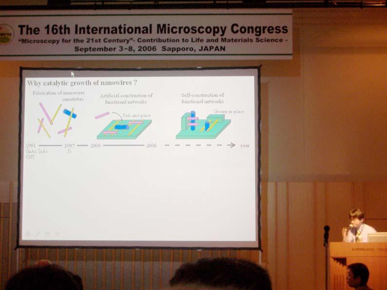
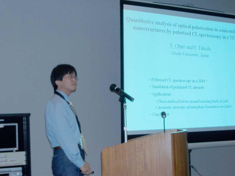
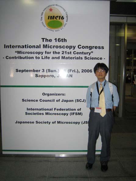
1 Quantitative analysis of optical polarization in semiconductor nanostructures by polarized cathodoluminescence spectroscopy in a transmission electron microscope Microstructure and optical properties of ZnSe nanowires grown on.znse(001) with Fe catalysts Formation mechanism of silicon surface manoholes Department of Physics, Graduate School of Science, Osaka University Assistant Professor Yutaka Ohno Oral Presentations at The 16th International Microscopy Congress September 3 8, 2006 Sapporo Convention Center, Sapporo, Hokkaido, Japan 21 st COE Program Towards a New Basic Science : Depth and Synthesis
2

 and nanowires, interact with polarized lights.")
3 Quantitative Analysis of Optical Polarization in Semiconductor Nanostructures by Polarized Cathodoluminescence Spectroscopy in a Transmission Electron Microscope Yutaka Ohno* and Seiji Takeda Department of Physics, Graduate School of Science, Osaka University, 1-1, Machikane-yama, Toyonaka, Osaka , JAPAN Optical properties in nanostructures have been of physical and technological interests since the properties are distinct from those of bulk crystals. Among them, optical polarization is an interesting topic. Nanostructures with anisotropic electronic structures, such as quantum wells (QWs) and nanowires, interact with polarized lights. For example, a QW emits a polarized light whose polarization direction is either parallel to or perpendicular to the well. From a viewpoint of technical interest, nanostructures emitting polarized light have potential application to future photonic nanodevices, such as polarization detectors and polarization threshold switches of nanometer size. Optical polarization in nanostructures was often studied by cathodoluminescence (CL) spectroscopy, since polarized CL light was obtained from a small space where a focused electron beam was illuminated. Polarized CL light was usually collected with a truncated ellipsoidal mirror equipped in an electron microscope, and the polarization of the collected light differed from one of the emitted light due to the effect of reflection on the mirror. So far, the reflection-effect was not fully taken into account. It has been shown that [1] optical polarization can be determined through the simulation of polarized CL intensities taken into account of the reflection-effect [FIG. 1]. By means of the method, and by using an apparatus designed especially for polarized CL spectroscopy in a transmission electron microscope (TEM) [2], optical polarization of semiconductor nanostructures has been examined quantitatively [e.g., 3-5]. Here we show a result concerning the nanostructures in a CuPt-ordered GaInP alloy. Cross-sectional scanning tunnelling microscopy on an alloy revealed that [3, 6] atomic layers of InP on (-111) and (-110), sandwiched between the ordered domains (about 2-10 nm in size), are formed. Polarized CL spectroscopy in a TEM revealed that [3] the InP layers act as QWs oriented on a slant with respect to the substrate and they emit lights linearly polarized parallel to the layers [FIG. 2]. The temperature-dependent intensity, polarization, and photon energy of the CL lights peaking below the band gap energy E g (at E g - 20 and E g - 33 mev) were expounded with the InP QW model. The method is also applied to examine the photo-induced stress in ZnSe due to photo-induced glide of stacking faults [4], anisotropic optical properties of multiple nanotwins in AlGaAs [5], etc. [1] Y. Ohno and S. Takeda, J. Electron Microsc. 51 (2002) 281. [2] Y. Ohno and S. Takeda, Rev. Sci. Instrum. 66 (1995) [3] Y. Ohno, Rhys. Rev. B 72 (2005) (R). [4] Y. Ohno, Appl. Phys. Lett. 87 (2005) [5] Y. Ohno, K. Shoda, S. Takeda, and N. Yamamoto, unpublished. [6] Y. Ohno, Jpn. J. Appl. Phys. 45(3B) (2006) [7] The author is indebted to Dr. K. Fujii of Tokyo University of Science for his supports. This work was partially supported by a Grant-in-Aid for Young Scientist (A) (# , ) from the Ministry of Education, Culture, Sports, Science and Technology. FIG. 1. Simulation of the polarized CL intensity of a (a) twoor (b) one-dimensional nanostructure measured with a truncated ellipsoidal mirror [1]. FIG. 2. (a) Experimental setup for polarized CL spectroscopy [3]. (b) Polarized CL spectra for various. (c) CL intensities vs.. The solid or broken curve is a calculated CL intensity for a QW on (-110) or (-111), respectively.

4 Microstructure and Optical Property of ZnSe Nanowires Grown on ZnSe(001) with Fe Catalysts Yutaka Ohno 1 *, Takeo Shirahama 1, Seiji Takeda 1, Atsushi Ishizumi 2, and Yoshihiko Kanemitsu 2,3 1 Department of Physics, Graduate School of Science, Osaka University, 1-1, Machikane-yama, Toyonaka, Osaka , JAPAN 2 Graduate School of Materials Science, Nara Institute of Science and Technology, Ikoma, Nara , JAPAN 3 Institute for Chemical Research, Kyoto University, Uji, Kyoto , JAPAN One-dimensional nanocrystals such as nanowires (NWs) have attracted a great deal of interest for applications in optoelectronics, etc. They have been frequently synthesized by the catalytic growth method, since we can grow NWs whose nucleation sites and sizes are precisely decided on a substrate by controlling those of catalysts [e.g., refs. 1 and 2], at temperatures much lower than the usual growth temperatures. By means of the method, ZnSe NWs can be grown on ZnSe(001) at low temperatures of K [3], which are comparable to the usual temperatures for fabrication of ZnSe-base optoelectronic devices [4], with proper catalysts of Fe nanoparticles. In this paper, we have determined in detail the microstructure and the optical property. ZnSe NWs were grown in a VG-80 chamber that is designed especially for growth of II-VI compound semiconductors by molecular-beam epitaxy [5]. A GaAs(001) wafer was installed into the chamber, and a ZnSe epilayer (about 90 nm thick) was grown on the wafer at the temperature of 573 K [5]. The wafer was cooled down to room temperature, and Fe atoms were evaporated on the epilayer, for fear that As and Ga atoms mix with the Fe deposit. The thickness was estimated to be about 1 nm. The deposited wafer was heated up to a growth temperature T g and maintained for a few min in order to generate Fe nanoparticles. Subsequently, NWs were grown at T g by the exposition of Zn and Se fluxes (the flow ratio of 1:2) simultaneously for 1 h. No NW grew at T g without the exposition. The structural nature was characterized by high-resolution transmission electron microscopy (HRTEM) with a JEOL JEM-2010 microscope operated at 160 kv and scanning electron microscopy (SEM) with a FEI Sirion 400 microscope operated at 3 kv [6]. The optical property was characterized with a photoluminescence (PL) spectroscopy system (the spectral resolution of ~3 mev), at temperatures in the range K. A large amount of NWs (the number density of the order of 10 9 cm -2 ) grew at the optimum temperature of T g = 573 K [FIG. 1(a)]. A NW tapered off to the top. The diameter at the top or the bottom was the order of 10 or 30 nm, respectively, and the typical length was about 200 nm. A NW was the zinc-blend structure, and it contained some stacking faults [FIG. 1(b)]. The longitudinal direction was <001>, <111>, <110>, or <112>. A nanoparticle that contains Fe, Zn, and Se atoms existed on the top of a NW, and no Fe atom was detected inside the NW. This result clearly shows that the NW grew via the vapor-liquid-solid mechanism [7]. NWs also grew at T g = 523 or 623 K, even though the number density was small. The NWs emitted excitonic PL light even at room temperature, due to high electronic quality. The temperature dependence of the linewidth, the peak energy, or the peak intensity of the PL light were examined [FIG. 2(a)], and the results were explained in terms of quantum confinement effects [e.g., FIG. 2(b)], as well as effects of structure inhomogeneity such as strain and stacking faults in NWs [8]. [1] J. Kikkawa, Y. Ohno, and S. Takeda, Appl. Phys. Lett. 86 (2005) [2] S. Takeda, K. Ueda, N. Ozaki, and Y. Ohno, Appl. Phys. Lett. 82 (2003) 979. [3] Y. Ohno, T. Shirahama, S. Takeda, A. Ishizumi, and Y. Kanemitsu, Appl. Phys. Lett. 87 (2005) [4] ZnSe nanowires have so far been grown on a substrate at temperatures above about K [3]. [5] Y. Ohno, N. Adachi, and S. Takeda, Appl. Phys. Lett. 83 (2003) 54. [6] SEM images were taken at FEI Company Japan Ltd. [7] R. S. Wagner and W. C. Ellis, Appl. Phys. Lett. 4 (1964) 89. [8] For example, Y. Kanemitsu, T. Nagai, Y. Yamada, and T. Taguchi, Appl. Phys. Lett. 82 (2003) 388. [9] This work was partially supported by a Grant-in-Aid for Young Scientist (A) (# , ) from the Ministry of Education, Culture, Sports, Science and Technology. FIG. 1. (a) SEM and (b) HRTEM images of NW [T g = 573 K]. FIG. 2. (a) PL spectra of a specimen grown at T g = 573 K at different temperatures. (b) Temperature dependence of the linewidth of the excitonic PL, defined as a full-width at the half-maximum (FWHM) of the luminescence. The solid line is the theoretical fit.

5 Formation Mechanism of Silicon Surface Nanoholes Yutaka Ohno 1 *, Seiji Takeda 1, Toshinari Ichihashi 2, and Sumio Iijima 2, 3 1 Department of Physics, Graduate School of Science, Osaka University, 1-1, Machikane-yama, Toyonaka, Osaka , JAPAN. 2 Fundamental Research Laboratories, NEC Corporation, 34 Miyukigaoka, Tsukuba, Ibaraki , JAPAN. 3 Meijo University, Shiogamaguchi, Tenpaku-ku, Nagoya , JAPAN. Nano-, meso-, and micro-porous materials have recently attracted considerable attention. Among them, allays of nanoholes on surfaces may be applied to optoelectronic devices, such as photonic waveguides and plasmonic integrated circuits, and also they may be used as templates for fabrication of useful nanostructures, catalysts for adsorption of gases, etc. Surface nanohole arrays can be formed by spontaneous fabrication techniques such as electron irradiation and electrochemical etching, etc., which have advantages in comparison with artificial techniques such as electron lithography, even though the formation mechanism is not fully understood. Here, surface nanohole arrays in silicon, formed spontaneously on electron exit surfaces of silicon foils via agglomeration of surface vacancies introduced under electron irradiation [1], are examined. The formation mechanism is studied by transmission electron microscopy (TEM) at an ultrahigh vacuum (UHV) and related techniques, since controlled clean surfaces can be provided and formation of nanostructures on the surfaces, on which an arbitrary number of surface vacancies are introduced intentionally, can be pursued. Nanoholes were formed on a clean deoxidized surface in an UHV microscope (the base pressure P ir ~1x10⁻⁸ Pa) or a surface virtually deoxidized in a conventional microscope [2] (P ir ~1x10⁻⁵ Pa) by electron irradiation. The electron flux f was the order of cm -2 s -1, and the electron energy was 200 kev. The electron dose D, f multiplied by the irradiation time, was up to about 2x10 24 cm -2. The nominal temperature during irradiation T ir ranged from room temperature to about 680 K in an UHV microscope, and from about 4 to 680 K in a conventional microscope. The irradiated surface was then observed by TEM with electrons of low flux, so that the surface was virtually kept unchanged during observation. The distribution of surface nanoholes is determined at the early stage of irradiation [4], and a nanohole is excavated, parallel to the irradiation direction, without changing the size of the opening under irradiation [1]. Therefore, only the formation process of two-dimensional patterns of nanoholes, which may be discussed by examining the size and spatial distribution of the openings of deep nanoholes after excavation, is taken into account at the stage. The experimental results were quantitatively explained with a classical phase separation model based on the migration of surface vacancies [3]. According to the model, the nearest-neighbor distance l nn [FIG. 1], the number density, and the average opening area of nanoholes followed Arrhenius law at high temperatures, and the activation energy for migration of surface vacancy under electron irradiation was estimated to be about 0.3 ev. After formation of two-dimensional patterns of surface nanoholes, only the excavation process, characterized by the depths, is taken into account. The depths of surface nanoholes can be estimated by three-dimensional TEM [e.g., FIGs. 2(a) and 2(b)], and so the excavation process can virtually be pursued. The typical excavation process [FIG. 2(c)] showed that surface nanoholes are excavated at a constant rate with increasing D [5]. The excavation rate was estimated at different experimental conditions, and the results were reproduced [5] with the model that a part of surface vacancies preferentially flow into nanoholes due to the momentums transferred from irradiating electrons [1]. [1] S. Takeda, K. Koto, S. Iijima, and T. Ichihashi, Phys. Rev. Lett. 79 (1997) [2] On surfaces in a conventional microscope, sputtering of surface atoms, oxidization, and contamination take place simultaneously under electron irradiation. When f is high, the first process is most probably predominant and so the surface is virtually free from oxidation and contamination [3]. [3] Y. Ohno, S. Takeda, T. Ichihashi, and S. Iijima, submitted. [4] N. Ozaki, Y. Ohno, M. Tanbara, D. Hamada, J. Yamasaki, and S. Takeda, Surf. Sci. 493 (2001) 547. [5] Y. Ohno, S. Takeda, T. Ichihashi, and S. Iijima, submitted. [6] This work was partially supported by a Grant-in-Aid for Scientific Research (A)(2) (# , ) and a Grant-in-Aid for Young Scientist (A) (# , ) from the Ministry of Education, Culture, Sports, Science and Technology. FIG. 1. T ir vs. l nn. Triangles, squares and circles mean the results for the nanoholes on {001}, {111} and {110}, respectively [closed triangles: P ir ~1x10⁻⁸ Pa, the other marks: P ir ~1x10⁻⁵ Pa]. FIG. 2. Surface nanoholes observed (a) parallel to and (b) normal to the irradiation direction. (c) D vs. the depths of nanoholes. The depths at an electron dose are slightly dispersed, and so each depth is plotted.
Fabrication at the nanoscale for nanophotonics
 Fabrication at the nanoscale for nanophotonics Ilya Sychugov, KTH Materials Physics, Kista silicon nanocrystal by electron beam induced deposition lithography Outline of basic nanofabrication methods Devices
III-V nanostructured materials synthesized by MBE droplet epitaxy
 III-V nanostructured materials synthesized by MBE droplet epitaxy E.A. Anyebe 1, C. C. Yu 1, Q. Zhuang 1,*, B. Robinson 1, O Kolosov 1, V. Fal ko 1, R. Young 1, M Hayne 1, A. Sanchez 2, D. Hynes 2, and
Nanostructure Fabrication Using Selective Growth on Nanosize Patterns Drawn by a Scanning Probe Microscope
 Nanostructure Fabrication Using Selective Growth on Nanosize Patterns Drawn by a Scanning Probe Microscope Kentaro Sasaki, Keiji Ueno and Atsushi Koma Department of Chemistry, The University of Tokyo,
Widely Tunable and Intense Mid-Infrared PL Emission from Epitaxial Pb(Sr)Te Quantum Dots in a CdTe Matrix
Te Quantum Dots in a CdTe Matrix") Widely Tunable and Intense Mid-Infrared PL Emission from Epitaxial Pb(Sr)Te Quantum Dots in a Matrix S. Kriechbaumer 1, T. Schwarzl 1, H. Groiss 1, W. Heiss 1, F. Schäffler 1,T. Wojtowicz 2, K. Koike 3,
Widely Tunable and Intense Mid-Infrared PL Emission from Epitaxial Pb(Sr)Te Quantum Dots in a Matrix S. Kriechbaumer 1, T. Schwarzl 1, H. Groiss 1, W. Heiss 1, F. Schäffler 1,T. Wojtowicz 2, K. Koike 3,
Physics and Material Science of Semiconductor Nanostructures
 Physics and Material Science of Semiconductor Nanostructures PHYS 570P Prof. Oana Malis Email: omalis@purdue.edu Course website: http://www.physics.purdue.edu/academic_programs/courses/phys570p/ 1 Course
Millimeter-Thick Single-Walled Carbon Nanotube Forests: Hidden Role of Catalyst Support
 Millimeter-Thick Single-Walled Carbon Nanotube Forests: Hidden Role of Catalyst Support Suguru Noda 1*, Kei Hasegawa 1, Hisashi Sugime 1, Kazunori Kakehi 1, Zhengyi Zhang 2, Shigeo Maruyama 2 and Yukio
ANTIMONY ENHANCED HOMOGENEOUS NITROGEN INCORPORATION INTO GaInNAs FILMS GROWN BY ATOMIC HYDROGEN-ASSISTED MOLECULAR BEAM EPITAXY
 ANTIMONY ENHANCED HOMOGENEOUS NITROGEN INCORPORATION INTO GaInNAs FILMS GROWN BY ATOMIC HYDROGEN-ASSISTED MOLECULAR BEAM EPITAXY Naoya Miyashita 1, Nazmul Ahsan 1, and Yoshitaka Okada 1,2 1. Research Center
Self-Assembled InAs Quantum Dots
 Self-Assembled InAs Quantum Dots Steve Lyon Department of Electrical Engineering What are semiconductors What are semiconductor quantum dots How do we make (grow) InAs dots What are some of the properties
Initial Emittance Measurements for Polarized Electron Gun with NEA-GaAs Type Photocathode
 Initial Emittance Measurements for Polarized Electron Gun with NEA-GaAs Type Photocathode Naoto Yamamoto*, M. Yamamoto*, R. Sakai*, T. Nakanishi*, S. Okumi*, M. Kuwahara*, K. Tamagaki*, T. Morino*, A.
Supplementary Figure 1 Detailed illustration on the fabrication process of templatestripped
 Supplementary Figure 1 Detailed illustration on the fabrication process of templatestripped gold substrate. (a) Spin coating of hydrogen silsesquioxane (HSQ) resist onto the silicon substrate with a thickness
Investigation of the bonding strength and interface current of p-siõn-gaas wafers bonded by surface activated bonding at room temperature
 Investigation of the bonding strength and interface current of p-siõn-gaas wafers bonded by surface activated bonding at room temperature M. M. R. Howlader, a) T. Watanabe, and T. Suga Research Center
Optical properties of nano-silicon
 Bull. Mater. Sci., Vol. 4, No. 3, June 001, pp. 85 89. Indian Academy of Sciences. Optical properties of nano-silicon S TRIPATHY, R K SONI*, S K GHOSHAL and K P JAIN Department of Physics, Indian Institute
MICRO-FOUR-POINT PROBES IN A UHV SCANNING ELECTRON MICROSCOPE FOR IN-SITU SURFACE-CONDUCTIVITY MEASUREMENTS
 Surface Review and Letters, Vol. 7, Nos. 5 & 6 (2000) 533 537 c World Scientific Publishing Company MICRO-FOUR-POINT PROBES IN A UHV SCANNING ELECTRON MICROSCOPE FOR IN-SITU SURFACE-CONDUCTIVITY MEASUREMENTS
Ultrafast single photon emitting quantum photonic structures. based on a nano-obelisk
 Ultrafast single photon emitting quantum photonic structures based on a nano-obelisk Je-Hyung Kim, Young-Ho Ko, Su-Hyun Gong, Suk-Min Ko, Yong-Hoon Cho Department of Physics, Graduate School of Nanoscience
Nanostructure. Materials Growth Characterization Fabrication. More see Waser, chapter 2
 Nanostructure Materials Growth Characterization Fabrication More see Waser, chapter 2 Materials growth - deposition deposition gas solid Physical Vapor Deposition Chemical Vapor Deposition Physical Vapor
Crystalline Surfaces for Laser Metrology
 Crystalline Surfaces for Laser Metrology A.V. Latyshev, Institute of Semiconductor Physics SB RAS, Novosibirsk, Russia Abstract: The number of methodological recommendations has been pronounced to describe
Level Repulsion of Localised Excitons Observed in Near-Field Photoluminescence Spectra
 phys. stat. sol. (a) 190, No. 3, 631 635 (2002) Level Repulsion of Localised Excitons Observed in Near-Field Photoluminescence Spectra A. Crottini (a), R. Idrissi Kaitouni (a), JL. Staehli 1 ) (a), B.
Lecture 3: Heterostructures, Quasielectric Fields, and Quantum Structures
 Lecture 3: Heterostructures, Quasielectric Fields, and Quantum Structures MSE 6001, Semiconductor Materials Lectures Fall 2006 3 Semiconductor Heterostructures A semiconductor crystal made out of more
Chapter 10. Nanometrology. Oxford University Press All rights reserved.
 Chapter 10 Nanometrology Oxford University Press 2013. All rights reserved. 1 Introduction Nanometrology is the science of measurement at the nanoscale level. Figure illustrates where nanoscale stands
Raman spectroscopy of self-assembled InAs quantum dots in wide-bandgap matrices of AlAs and aluminium oxide
 Mat. Res. Soc. Symp. Proc. Vol. 737 2003 Materials Research Society E13.8.1 Raman spectroscopy of self-assembled InAs quantum dots in wide-bandgap matrices of AlAs and aluminium oxide D. A. Tenne, A. G.
CHAPTER 3. OPTICAL STUDIES ON SnS NANOPARTICLES
 42 CHAPTER 3 OPTICAL STUDIES ON SnS NANOPARTICLES 3.1 INTRODUCTION In recent years, considerable interest has been shown on semiconducting nanostructures owing to their enhanced optical and electrical
Optical Characterization of Self-Assembled Si/SiGe Nano-Structures
 Optical Characterization of Self-Assembled Si/SiGe Nano-Structures T. Fromherz, W. Mac, G. Bauer Institut für Festkörper- u. Halbleiterphysik, Johannes Kepler Universität Linz, Altenbergerstraße 69, A-
Emission Spectra of the typical DH laser
 Emission Spectra of the typical DH laser Emission spectra of a perfect laser above the threshold, the laser may approach near-perfect monochromatic emission with a spectra width in the order of 1 to 10
Quantum Dot Lasers. Jose Mayen ECE 355
 Quantum Dot Lasers Jose Mayen ECE 355 Overview of Presentation Quantum Dots Operation Principles Fabrication of Q-dot lasers Advantages over other lasers Characteristics of Q-dot laser Types of Q-dot lasers
Novel materials and nanostructures for advanced optoelectronics
 Novel materials and nanostructures for advanced optoelectronics Q. Zhuang, P. Carrington, M. Hayne, A Krier Physics Department, Lancaster University, UK u Brief introduction to Outline Lancaster University
Physics and Material Science of Semiconductor Nanostructures
 Physics and Material Science of Semiconductor Nanostructures PHYS 570P Prof. Oana Malis Email: omalis@purdue.edu Course website: http://www.physics.purdue.edu/academic_programs/courses/phys570p/ Lecture
Nanofabrication/Nano-Characterization Calixarene and CNT Control Technology
 Nanofabrication/Nano-Characterization Calixarene and CNT Control Technology ISHIDA Masahiko, FUJITA Junichi, NARIHIRO Mitsuru, ICHIHASHI Toshinari, NIHEY Fumiyuki, OCHIAI Yukinori Abstract The world of
Seminars in Nanosystems - I
 Seminars in Nanosystems - I Winter Semester 2011/2012 Dr. Emanuela Margapoti Emanuela.Margapoti@wsi.tum.de Dr. Gregor Koblmüller Gregor.Koblmueller@wsi.tum.de Seminar Room at ZNN 1 floor Topics of the
Raman spectral study of silicon nanowires: High-order scattering and phonon confinement effects
 PHYSICAL REVIEW B VOLUME 61, NUMBER 24 Raman spectral study of silicon nanowires: High-order scattering and phonon confinement effects 15 JUNE 2000-II Rong-ping Wang Laboratory of Optical Physics, Institute
Micro-patterned porous silicon using proton beam writing
 Micro-patterned porous silicon using proton beam writing M. B. H. Breese, D. Mangaiyarkarasi, E. J. Teo*, A. A. Bettiol and D. Blackwood* Centre for Ion Beam Applications, Department of Physics, National
The first three categories are considered a bottom-up approach while lithography is a topdown
 Nanowires and Nanorods One-dimensional structures have been called in different ways: nanowires, nanorod, fibers of fibrils, whiskers, etc. The common characteristic of these structures is that all they
Superconducting Single-photon Detectors
 : Quantum Cryptography Superconducting Single-photon Detectors Hiroyuki Shibata Abstract This article describes the fabrication and properties of a single-photon detector made of a superconducting NbN
Semiconductor Physics and Devices
 Syllabus Advanced Nano Materials Semiconductor Physics and Devices Textbook Donald A. Neamen (McGraw-Hill) Semiconductor Physics and Devices Seong Jun Kang Department of Advanced Materials Engineering
Mechanisms of Visible Photoluminescence from Size-Controlled Silicon Nanoparticles
 Mat. Res. Soc. Symp. Proc. Vol. 737 23 Materials Research Society F1.5.1 Mechanisms of Visible Photoluminescence from Size-Controlled Silicon Nanoparticles Toshiharu Makino *, Nobuyasu Suzuki, Yuka Yamada,
Graphene Fundamentals and Emergent Applications
 Graphene Fundamentals and Emergent Applications Jamie H. Warner Department of Materials University of Oxford Oxford, UK Franziska Schaffel Department of Materials University of Oxford Oxford, UK Alicja
Supporting Information s for
 Supporting Information s for # Self-assembling of DNA-templated Au Nanoparticles into Nanowires and their enhanced SERS and Catalytic Applications Subrata Kundu* and M. Jayachandran Electrochemical Materials
Recent PES Photocathode R&D at Nagoya University
 Recent PES Photocathode R&D at Nagoya University M. Kuwahara, T. Nishitani a, T. Nakanishi, S. Okumi, M. Yamamoto, F. Furuta, M.Miyamoto, N. Yamamoto, K. Naniwa, K. Yasui, K. Yamaguchi b, O. Watanabe c,
Temperature Dependent Optical Band Gap Measurements of III-V films by Low Temperature Photoluminescence Spectroscopy
 Temperature Dependent Optical Band Gap Measurements of III-V films by Low Temperature Photoluminescence Spectroscopy Linda M. Casson, Francis Ndi and Eric Teboul HORIBA Scientific, 3880 Park Avenue, Edison,
LOW-TEMPERATURE Si (111) HOMOEPITAXY AND DOPING MEDIATED BY A MONOLAYER OF Pb
 HOMOEPITAXY AND DOPING MEDIATED BY A MONOLAYER OF Pb") LOW-TEMPERATURE Si (111) HOMOEPITAXY AND DOPING MEDIATED BY A MONOLAYER OF Pb O.D. DUBON, P.G. EVANS, J.F. CHERVINSKY, F. SPAEPEN, M.J. AZIZ, and J.A. GOLOVCHENKO Division of Engineering and Applied Sciences,
LOW-TEMPERATURE Si (111) HOMOEPITAXY AND DOPING MEDIATED BY A MONOLAYER OF Pb O.D. DUBON, P.G. EVANS, J.F. CHERVINSKY, F. SPAEPEN, M.J. AZIZ, and J.A. GOLOVCHENKO Division of Engineering and Applied Sciences,
Recent Status of Polarized Electron Sources at Nagoya University
 Recent Status of Polarized Electron Sources at Nagoya University M. Kuwahara, N. Yamamoto, F. Furuta, T. Nakanishi, S. Okumi, M. Yamamoto, M. Kuriki *, T. Ujihara ** and K. Takeda ** Graduate School of
Nano and micro Hall-effect sensors for room-temperature scanning hall probe microscopy
 Microelectronic Engineering 73 74 (2004) 524 528 www.elsevier.com/locate/mee Nano and micro Hall-effect sensors for room-temperature scanning hall probe microscopy A. Sandhu a, *, A. Okamoto b, I. Shibasaki
Carbon Nanotube: The Inside Story
 Krasnoyarsk: 24 th August, 2009 Carbon Nanotube: The Inside Story Review written for Journal of Nanoscience and Nanotechnology Yoshinori ANDO Dean of Faculty of Science and Technology, Meijo University
Supplementary information
 Supplementary information Electrochemical synthesis of metal and semimetal nanotube-nanowire heterojunctions and their electronic transport properties Dachi Yang, ab Guowen Meng,* a Shuyuan Zhang, c Yufeng
In situ electron-beam processing for III-V semiconductor nanostructure fabrication
 In situ electron-beam processing for III-V semiconductor nanostructure fabrication Tomonori Ishikawa a), Shigeru Kohmoto, Tetsuya Nishimura*, and Kiyoshi Asakawa The Femtosecond Technology Research Association
Nanowires and nanorods
 Nanowires and nanorods One-dimensional structures have been called in different ways: nanowires, nanorod, fibers of fibrils, whiskers, etc. These structures have a nanometer size in one of the dimensions,
SYNTHESIS OF CADMIUM SULFIDE NANOSTRUCTURES BY NOVEL PRECURSOR
 Nanomaterials: Applications and Properties (NAP-2011). Vol. 1, Part I 107 SYNTHESIS OF CADMIUM SULFIDE NANOSTRUCTURES BY NOVEL PRECURSOR M. Salavati Niasari 1,2* 1 Department of Inorganic Chemistry, Faculty
Electroluminescence from Silicon and Germanium Nanostructures
 Electroluminescence from silicon Silicon Getnet M. and Ghoshal S.K 35 ORIGINAL ARTICLE Electroluminescence from Silicon and Germanium Nanostructures Getnet Melese* and Ghoshal S. K.** Abstract Silicon
Luminescence basics. Slide # 1
 Luminescence basics Types of luminescence Cathodoluminescence: Luminescence due to recombination of EHPs created by energetic electrons. Example: CL mapping system Photoluminescence: Luminescence due to
Two-Photon Fabrication of Three-Dimensional Metallic Nanostructures for Plasmonic Metamaterials
 Two-Photon Fabrication of Three-Dimensional Metallic Nanostructures for Plasmonic Metamaterials Atsushi ISHIKAWA 1 and Takuo TANAKA 1,2 1- Metamaterials Laboratory, RIKEN, 2-1 Hirosawa, Wako, Saitama 351-0198,
Optical Investigation of the Localization Effect in the Quantum Well Structures
 Department of Physics Shahrood University of Technology Optical Investigation of the Localization Effect in the Quantum Well Structures Hamid Haratizadeh hamid.haratizadeh@gmail.com IPM, SCHOOL OF PHYSICS,
solidi current topics in solid state physics InAs quantum dots grown by molecular beam epitaxy on GaAs (211)B polar substrates
B polar substrates") solidi status physica pss c current topics in solid state physics InAs quantum dots grown by molecular beam epitaxy on GaAs (211)B polar substrates M. Zervos1, C. Xenogianni1,2, G. Deligeorgis1, M. Androulidaki1,
solidi status physica pss c current topics in solid state physics InAs quantum dots grown by molecular beam epitaxy on GaAs (211)B polar substrates M. Zervos1, C. Xenogianni1,2, G. Deligeorgis1, M. Androulidaki1,
Nanostrukturphysik (Nanostructure Physics)
") Nanostrukturphysik (Nanostructure Physics) Prof. Yong Lei & Dr. Yang Xu Fachgebiet 3D-Nanostrukturierung, Institut für Physik Contact: yong.lei@tu-ilmenau.de; yang.xu@tu-ilmenau.de Office: Unterpoerlitzer
Nanostrukturphysik (Nanostructure Physics) Prof. Yong Lei & Dr. Yang Xu Fachgebiet 3D-Nanostrukturierung, Institut für Physik Contact: yong.lei@tu-ilmenau.de; yang.xu@tu-ilmenau.de Office: Unterpoerlitzer
ABNORMAL X-RAY EMISSION FROM INSULATORS BOMBARDED WITH LOW ENERGY IONS
 302 ABNORMAL X-RAY EMISSION FROM INSULATORS BOMBARDED WITH LOW ENERGY IONS M. Song 1, K. Mitsuishi 1, M. Takeguchi 1, K. Furuya 1, R. C. Birtcher 2 1 High Voltage Electron Microscopy Station, National
Development of a nanostructural microwave probe based on GaAs
 Microsyst Technol (2008) 14:1021 1025 DOI 10.1007/s00542-007-0484-0 TECHNICAL PAPER Development of a nanostructural microwave probe based on GaAs Y. Ju Æ T. Kobayashi Æ H. Soyama Received: 18 June 2007
Observation of charged excitons in hole-doped carbon nanotubes using photoluminescence and absorption spectroscopy
 Observation of charged excitons in hole-doped carbon nanotubes using photoluminescence and absorption spectroscopy Ryusuke Matsunaga 1, Kazunari Matsuda 1, and Yoshihiko Kanemitsu 1,2 1 Institute for Chemical
Gold nanothorns macroporous silicon hybrid structure: a simple and ultrasensitive platform for SERS
 Supporting Information Gold nanothorns macroporous silicon hybrid structure: a simple and ultrasensitive platform for SERS Kamran Khajehpour,* a Tim Williams, b,c Laure Bourgeois b,d and Sam Adeloju a
Special Properties of Au Nanoparticles
 Special Properties of Au Nanoparticles Maryam Ebrahimi Chem 7500/750 March 28 th, 2007 1 Outline Introduction The importance of unexpected electronic, geometric, and chemical properties of nanoparticles
Part I. Nanostructure design and structural properties of epitaxially grown quantum dots and nanowires
 Part I Nanostructure design and structural properties of epitaxially grown quantum dots and nanowires 1 Growth of III V semiconductor quantum dots C. Schneider, S. Höfling and A. Forchel 1.1 Introduction
Nova 600 NanoLab Dual beam Focused Ion Beam IITKanpur
 Nova 600 NanoLab Dual beam Focused Ion Beam system @ IITKanpur Dual Beam Nova 600 Nano Lab From FEI company (Dual Beam = SEM + FIB) SEM: The Electron Beam for SEM Field Emission Electron Gun Energy : 500
Self-Assembled InAs Quantum Dots on Patterned InP Substrates
 Self-Assembled InAs Quantum Dots on Patterned InP Substrates J. Lefebvre, P.J. Poole, J. Fraser, G.C. Aers, D. Chithrani, and R.L. Williams Institute for Microstructural Sciences, National Research Council
GaAs and InGaAs Single Electron Hex. Title. Author(s) Kasai, Seiya; Hasegawa, Hideki. Citation 13(2-4): Issue Date DOI
 Kasai, Seiya; Hasegawa, Hideki. Citation 13(2-4): Issue Date DOI") Title GaAs and InGaAs Single Electron Hex Circuits Based on Binary Decision D Author(s) Kasai, Seiya; Hasegawa, Hideki Citation Physica E: Low-dimensional Systems 3(2-4): 925-929 Issue Date 2002-03 DOI
Title GaAs and InGaAs Single Electron Hex Circuits Based on Binary Decision D Author(s) Kasai, Seiya; Hasegawa, Hideki Citation Physica E: Low-dimensional Systems 3(2-4): 925-929 Issue Date 2002-03 DOI
Semiconductor Nanowires: Motivation
 Semiconductor Nanowires: Motivation Patterning into sub 50 nm range is difficult with optical lithography. Self-organized growth of nanowires enables 2D confinement of carriers with large splitting of
Defense Technical Information Center Compilation Part Notice
 UNCLASSIFIED Defense Technical Information Center Compilation Part Notice ADP013064 TITLE: Apparent Microcavity Effect in the Near-Field Photoluminescence f a Single Quantum Dot DISTRIBUTION: Approved
SUPPLEMENTARY INFORMATION
 SUPPLEMENTARY INFORMATION DOI: 10.1038/NNANO.2012.63 Bright infrared quantum-dot light-emitting diodes through inter-dot spacing control Liangfeng Sun, Joshua J. Choi, David Stachnik, Adam C. Bartnik,
Plan for Lectures #4, 5, & 6. Theme Of Lectures: Nano-Fabrication
 Plan for Lectures #4, 5, & 6 Theme Of Lectures: Nano-Fabrication Quantum Wells, SLs, Epitaxial Quantum Dots Carbon Nanotubes, Semiconductor Nanowires Self-assembly and Self-organization Two Approaches
Nanosphere Lithography
 Nanosphere Lithography Derec Ciafre 1, Lingyun Miao 2, and Keita Oka 1 1 Institute of Optics / 2 ECE Dept. University of Rochester Abstract Nanosphere Lithography is quickly emerging as an efficient, low
There's Plenty of Room at the Bottom
 There's Plenty of Room at the Bottom 12/29/1959 Feynman asked why not put the entire Encyclopedia Britannica (24 volumes) on a pin head (requires atomic scale recording). He proposed to use electron microscope
Nanoelectronics 09. Atsufumi Hirohata Department of Electronics. Quick Review over the Last Lecture
 Nanoelectronics 09 Atsufumi Hirohata Department of Electronics 13:00 Monday, 12/February/2018 (P/T 006) Quick Review over the Last Lecture ( Field effect transistor (FET) ): ( Drain ) current increases
Strong light matter coupling in two-dimensional atomic crystals
 SUPPLEMENTARY INFORMATION DOI: 10.1038/NPHOTON.2014.304 Strong light matter coupling in two-dimensional atomic crystals Xiaoze Liu 1, 2, Tal Galfsky 1, 2, Zheng Sun 1, 2, Fengnian Xia 3, Erh-chen Lin 4,
X- ray Photoelectron Spectroscopy and its application in phase- switching device study
 X- ray Photoelectron Spectroscopy and its application in phase- switching device study Xinyuan Wang A53073806 I. Background X- ray photoelectron spectroscopy is of great importance in modern chemical and
Supplementary Information for
 Supplementary Information for Multi-quantum well nanowire heterostructures for wavelength-controlled lasers Fang Qian 1, Yat Li 1 *, Silvija Gradečak 1, Hong-Gyu Park 1, Yajie Dong 1, Yong Ding 2, Zhong
MEMS Metrology. Prof. Tianhong Cui ME 8254
 MEMS Metrology Prof. Tianhong Cui ME 8254 What is metrology? Metrology It is the science of weights and measures Refers primarily to the measurements of length, weight, time, etc. Mensuration- A branch
Quantum Condensed Matter Physics Lecture 12
 Quantum Condensed Matter Physics Lecture 12 David Ritchie QCMP Lent/Easter 2016 http://www.sp.phy.cam.ac.uk/drp2/home 12.1 QCMP Course Contents 1. Classical models for electrons in solids 2. Sommerfeld
Chapter 103 Spin-Polarized Scanning Tunneling Microscopy
 Chapter 103 Spin-Polarized Scanning Tunneling Microscopy Toyo Kazu Yamada Keywords Spin-polarized tunneling current Spin polarization Magnetism 103.1 Principle Spin-polarized scanning tunneling microscopy
Spectroscopy at nanometer scale
 Spectroscopy at nanometer scale 1. Physics of the spectroscopies 2. Spectroscopies for the bulk materials 3. Experimental setups for the spectroscopies 4. Physics and Chemistry of nanomaterials Various
Light-Induced Atom Desorption in Alkali Vapor Cells
 Fundamental Physics Using Atoms, 2010/08/09, Osaka Light-Induced Atom Desorption in Alkali Vapor Cells A. Hatakeyama (Tokyo Univ. Agr. Tech.) K. Hosumi K. Kitagami Alkali vapor cells UHV cell for laser
Structural and Optical Properties of III-III-V-N Type
 i Structural and Optical Properties of III-III-V-N Type Alloy Films and Their Quantum Wells ( III-III-V- N 型混晶薄膜および量子井戸の構造的および光学的性質 ) This dissertation is submitted as a partial fulfillment of the requirements
GISAXS, GID and X-Ray Reflectivity in Materials Science
 united nations educational, scientific and cultural organization the abdus salam international centre for theoretical physics international atomic energy agency SCHOOL ON SYNCHROTRON RADIATION AND APPLICATIONS
CITY UNIVERSITY OF HONG KONG. Theoretical Study of Electronic and Electrical Properties of Silicon Nanowires
 CITY UNIVERSITY OF HONG KONG Ë Theoretical Study of Electronic and Electrical Properties of Silicon Nanowires u Ä öä ªqk u{ Submitted to Department of Physics and Materials Science gkö y in Partial Fulfillment
Extreme band bending at MBE-grown InAs(0 0 1) surfaces induced by in situ sulphur passivation
 surfaces induced by in situ sulphur passivation") Journal of Crystal Growth 237 239 (2002) 196 200 Extreme band bending at MBE-grown InAs(0 0 1) surfaces induced by in situ sulphur passivation M.J. Lowe a, T.D. Veal a, C.F. McConville a, G.R. Bell b,
Journal of Crystal Growth 237 239 (2002) 196 200 Extreme band bending at MBE-grown InAs(0 0 1) surfaces induced by in situ sulphur passivation M.J. Lowe a, T.D. Veal a, C.F. McConville a, G.R. Bell b,
Characterisation of Nanoparticle Structure by High Resolution Electron Microscopy
 Journal of Physics: Conference Series OPEN ACCESS Characterisation of Nanoparticle Structure by High Resolution Electron Microscopy To cite this article: Robert D Boyd et al 2014 J. Phys.: Conf. Ser. 522
Chemical Analysis in TEM: XEDS, EELS and EFTEM. HRTEM PhD course Lecture 5
 Chemical Analysis in TEM: XEDS, EELS and EFTEM HRTEM PhD course Lecture 5 1 Part IV Subject Chapter Prio x-ray spectrometry 32 1 Spectra and mapping 33 2 Qualitative XEDS 34 1 Quantitative XEDS 35.1-35.4
Debjit Roy, Saptarshi Mandal, Chayan K. De, Kaushalendra Kumar and Prasun K. Mandal*
 Electronic Supplementary Material (ESI) for Physical Chemistry Chemical Physics. This journal is the Owner Societies 2018 Nearly Suppressed Photoluminescence Blinking of Small Sized, Blue-Green-Orange-Red
City University of Hong Kong. Course Syllabus. offered by Department of Physics and Materials Science with effect from Semester A 2016 / 17
 City University of Hong Kong offered by Department of Physics and Materials Science with effect from Semester A 2016 / 17 Part I Course Overview Course Title: Nanostructures and Nanotechnology Course Code:
Semiconductor Quantum Dot Nanostructures and their Roles in the Future of Photonics
 550 Brazilian Journal of Physics, vol. 34, no. 2B, June, 2004 Semiconductor Quantum Dot Nanostructures and their Roles in the Future of Photonics S. Fafard, K. Hinzer, and C. N. Allen Institute for Microstructural
GRAPHENE ON THE Si-FACE OF SILICON CARBIDE USER MANUAL
 GRAPHENE ON THE Si-FACE OF SILICON CARBIDE USER MANUAL 1. INTRODUCTION Silicon Carbide (SiC) is a wide band gap semiconductor that exists in different polytypes. The substrate used for the fabrication
1. Introduction A technique has been developed for investigating electric-field distributions of optical antennas in the depth direction by means of a
 Probing enhancement of an electric field perpendicular to an optical antenna surface using SiC surface phonon polaritons J. Miyata 1, Y. Yamamoto 1, Y. Kunichika 1, T. Kawano 1, N. Umemori 1, K. Kasahara
Fabrication and Domain Imaging of Iron Magnetic Nanowire Arrays
 Abstract #: 983 Program # MI+NS+TuA9 Fabrication and Domain Imaging of Iron Magnetic Nanowire Arrays D. A. Tulchinsky, M. H. Kelley, J. J. McClelland, R. Gupta, R. J. Celotta National Institute of Standards
Three-Dimensional Silicon-Germanium Nanostructures for Light Emitters and On-Chip Optical. Interconnects
 Three-Dimensional Silicon-Germanium Nanostructures for Light Emitters and On-Chip Optical eptember 2011 Interconnects Leonid Tsybeskov Department of Electrical and Computer Engineering New Jersey Institute
Possibility of Exciton Mediated Superconductivity in Nano-Sized Sn/Si Core-Shell
 Possibility of Exciton Mediated Superconductivity in Nano-Sized Sn/Si Core-Shell Clusters: A Process Technology towards Heterogeneous Material in Nano-Scale Yuichiro Kurokawa, Takehiko Hihara, Ikuo Ichinose
Photonic Crystal Nanocavities for Efficient Light Confinement and Emission
 Journal of the Korean Physical Society, Vol. 42, No., February 2003, pp. 768 773 Photonic Crystal Nanocavities for Efficient Light Confinement and Emission Axel Scherer, T. Yoshie, M. Lončar, J. Vučković
OPTI510R: Photonics. Khanh Kieu College of Optical Sciences, University of Arizona Meinel building R.626
 OPTI510R: Photonics Khanh Kieu College of Optical Sciences, University of Arizona kkieu@optics.arizona.edu Meinel building R.626 Announcements HW#3 is assigned due Feb. 20 st Mid-term exam Feb 27, 2PM
Precise control of size and density of self-assembled Ge dot on Si(1 0 0) by carbon-induced strain-engineering
 by carbon-induced strain-engineering") Applied Surface Science 216 (2003) 419 423 Precise control of size and density of self-assembled Ge dot on Si(1 0 0) by carbon-induced strain-engineering Y. Wakayama a,*, L.V. Sokolov b, N. Zakharov c,
Applied Surface Science 216 (2003) 419 423 Precise control of size and density of self-assembled Ge dot on Si(1 0 0) by carbon-induced strain-engineering Y. Wakayama a,*, L.V. Sokolov b, N. Zakharov c,
PHOTOLUMINESCENCE STUDY OF INGAAS/GAAS QUANTUM DOTS
 PHOTOLUMINESCENCE STUDY OF INGAAS/GAAS QUANTUM DOTS A. Majid a,b, Samir Alzobaidi a and Thamer Alharbi a a Department of Physics, College of Science, Almajmaah University, P. O. Box no.1712, Al-Zulfi 11932,
Electronic Supplementary Information
 Electronic Supplementary Information High Electrocatalytic Activity of Self-standing Hollow NiCo 2 S 4 Single Crystalline Nanorod Arrays towards Sulfide Redox Shuttles in Quantum Dot-sensitized Solar Cells
Local Atomic Structure and Electronic State of ZnS Films Synthesized by Using CBD Technique
 Materials Transactions, Vol. 43, No. 7 (2002) pp. 1512 to 1516 Special Issue on Grain Boundaries, Interfaces, Defects and Localized Quantum Structures in Ceramics c 2002 The Japan Institute of Metals Local
M R S Internet Journal of Nitride Semiconductor Research
 M R S Internet Journal of Nitride Semiconductor Research Volume 2, Article 25 Properties of the Biexciton and the Electron-Hole-Plasma in Highly Excited GaN J.-Chr. Holst, L. Eckey, A. Hoffmann, I. Broser
Electrochemical Deposition of Iron Nanoparticles on PPY and H terminated Si substrates. Karan Sukhija Co-op Term # 1 April 28 th, 2005
 Electrochemical Deposition of Iron Nanoparticles on PPY and H terminated Si substrates Karan Sukhija Co-op Term # 1 April 28 th, 2005 Future Suggested Experiments Acknowledgments Presentation Outline Background
Nanomaterials and their Optical Applications
 Nanomaterials and their Optical Applications Winter Semester 2013 Lecture 02 rachel.grange@uni-jena.de http://www.iap.uni-jena.de/multiphoton Lecture 2: outline 2 Introduction to Nanophotonics Theoretical
what happens if we make materials smaller?
 what happens if we make materials smaller? IAP VI/10 ummer chool 2007 Couvin Prof. ns outline Introduction making materials smaller? ynthesis how do you make nanomaterials? Properties why would you make