Visualizing the atomic scale electronic structure of the Ca 2 CuO 2 Cl 2 Mott insulator
|
|
|
- Aron McDowell
- 5 years ago
- Views:
Transcription
1 Visualizing the atomic scale electronic structure of the Ca 2 CuO 2 Cl 2 Mott insulator Cun Ye 1,*, Peng Cai 1,*, Runze Yu 2, Xiaodong Zhou 1, Wei Ruan 1, Qingqing Liu 2, Changqing Jin 2 & Yayu Wang 1, 1 State Key Laboratory of Low Dimensional Quantum Physics, Department of Physics, Tsinghua University, Beijing , China 2 Institute of Physics, Chinese Academy of Sciences, Beijing , China * These authors contributed equally to this work. yayuwang@tsinghua.edu.cn
2 Although the mechanism of superconductivity in the cuprates remains elusive, it is generally agreed that at the heart of the problem is the physics of doped Mott insulators 1. The cuprate parent compound has one unpaired electron per Cu site, and is predicted by band theory to be a half-filled metal. The strong onsite Coulomb repulsion, however, prohibits electron hopping between neighboring sites and leads to a Mott insulator ground state with antiferromagnetic (AF) ordering 2. Charge carriers doped into the CuO 2 plane destroy the insulating phase and superconductivity emerges as the carrier density is sufficiently high. The natural starting point for tackling high T C superconductivity is to elucidate the electronic structure of the parent Mott insulator and the behavior of a single doped charge. Here we use a scanning tunneling microscope to investigate the atomic scale electronic structure of the Ca 2 CuO 2 Cl 2 parent Mott insulator of the cuprates. The full electronic spectrum across the Mott-Hubbard gap is uncovered for the first time, which reveals the particle-hole symmetric and spatially uniform Hubbard bands. A single electron donated by surface defect is found to create a broad in-gap electronic state that is strongly localized in space with spatial characteristics intimately related to the AF spin background. The unprecedented real space electronic structure of the parent cuprate sheds important new light on the origin of high T C superconductivity from the doped Mott insulator perspective. Despite extensive experimental studies on parent and lightly doped Mott insulators, a comprehensive picture about their electronic structure is still lacking. Optical spectroscopy 3 and resonant inelastic x-ray spectroscopy (RIXS) 4-6 can probe the excitations across the Mott-Hubbard gap, but they cannot detect the ground state electronic structure directly.
3 Angle-resolved photoemission spectroscopy (ARPES) provides direct momentum (k) space structure of the occupied lower Hubbard band (LHB) 7-9, but is unable to reach the empty states above the Fermi level (E F ), leaving the upper Hubbard band (UHB) unexplored. The lack of complete spectroscopic information across the Mott-Hubbard gap makes it difficult to clarify how the high energy spectral weight is transferred to the low energy states near E F, upon which superconductivity emerges. Another vital piece of information that is still missing is the spatial characteristic of the Mott insulator electronic structure. Because the Mott physics is dictated by onsite Coulomb repulsion, the real space picture could be more relevant than the k-space picture, which has been extremely successful in describing weakly-interacting electron systems. Especially, atomic scale resolution becomes indispensible if we want to experimentally illustrate the electronic properties of a single charge doped into the AF background. Scanning tunneling microscopy (STM) is an ideal spectroscopic technique for filling the aforementioned gaps in our understanding of doped Mott insulators. STM can directly map out the electronic states both below and above E F, with the unique capability of atomic scale spatial resolution. STM studies on high T C cuprates have revealed a variety of remarkable phenomena including the impurity resonance 10,11, checkerboard-like ordering 12-15, phase incoherent pairing 16,17, and quasiparticle interference 18. However, the parent Mott insulator phase has never been investigated by STM, most likely due to the technical challenges associated with tunneling into a good insulator. Our recent advance in STM measurements at relatively high temperature and over large bias range enables the atomic scale studies of the parent Mott insulator, as described in the Method Summary.
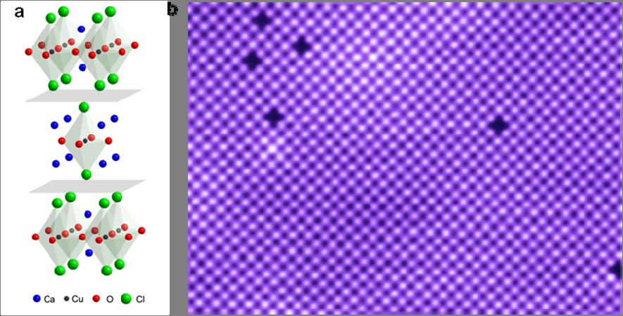
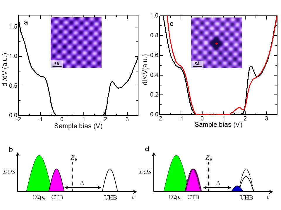
4 The oxychloride cuprate Ca 2 CuO 2 Cl 2 (CCOC) parent Mott insulator is chosen for its high crystal quality and excellent surface property. Figure 1a shows the schematic crystal structure of CCOC, which is similar to that of the prototypical parent compound La 2 CuO 4. The crystal cleaves easily between two adjacent CaCl layers, exposing the Cl terminated surface. The CuO 2 plane lies at 2.73Å below the surface and the Cu sites are directly underneath the exposed apical Cl atoms. Figure 1b displays a typical STM topography of cleaved CCOC taken at T = 77K with sample bias V s = -3.5V and tunneling current I t = 10pA, which reveals a large area of atomically flat terrace. The Cl atoms form a regular square lattice with lattice constant a ~ 3.9Å, in agreement with the tetragonal unit cell of CCOC. The cross-shaped dark spots in the image correspond to the missing Cl defects, which are created during the cleaving process. The inset of Fig. 2a displays the high resolution STM image of a defect-free area of CCOC, which has arguably the most ideal surface structure for the cuprates without any complication from structural supermodulations and electronic inhomogeneities. The local electronic structure of CCOC is probed by di/dv (differential conductance) spectroscopy. Figure 2a displays the spatially averaged di/dv curve obtained on the surface shown in the inset, which uncovers the full electronic spectrum across the Mott-Hubbard gap. The occupied state di/dv curve is very similar to the ARPES measured energy distribution curve of CCOC 8,19. Since the parent cuprate is a charge transfer insulator with oxygen bands lying between the lower and upper Hubbard bands 20, the shoulder near V s = -0.8V is ascribed to the charge transfer band (CTB) and the rapid increase for V s < -2.0V is due to the nonbonding O 2p π state 8,19. The di/dv of the CTB can be fit well by a Gaussian lineshape (Fig. S2a) with the full-width at half-maximum (FWHM) Γ = 0.47V, which is in rough agreement
5 with the bandwidth W = 0.35eV determined by the ARPES band dispersion 19. The totally new feature revealed by Fig. 2a is the UHB above E F, which was an unexplored territory before this report. The UHB also shows a Gaussian-like profile that peaks around V s = 2.3V with Γ = 0.34eV (Fig. S2b). The simultaneous observation of CTB and UHB immediately reveals several key spectroscopic features of the Mott insulator phase. The effective Mott-Hubbard gap, or more precisely the charge transfer gap, can be directly measured to be Δ = 2.2eV. This value is in good agreement with that obtained by optical spectroscopy and RIXS on parent CCOC 5. The E F lies near the CTB edge, as has been seen in the ARPES results 19, due to the hole-type carriers in the bulk induced by defects. The di/dv lineshape and peak value of the CTB and UHB are very similar to each other, indicating approximate particle-hole symmetry across the charge transfer gap. The electronic structure of the Mott insulator phase is schematically illustrated in Fig. 2b. We next turn to the spatial distribution of the electronic structure. Since the lowest energy excitation of the charge transfer insulator is the removal of an electron from the occupied O 2p orbital to the unoccupied Cu 3d 2 2 x y orbital 20, naïvely it is expected that the unpaired hole will mainly reside on the anion ligands and electron on the cation d orbitals 21. This picture implies that the relative weight of CTB and UHB should vary between the Cu and O sites. However, our atomically resolved di/dv spectroscopy shows that the entire electronic structure is highly uniform in space without significant difference between the Cu, O, and Ca sites (Fig. S3). This suggests that both the CTB and UHB of parent cuprate form extended states in space rather than keeping their local orbital characteristics. Now that the electronic structure of pristine CCOC is well established, we are ready to
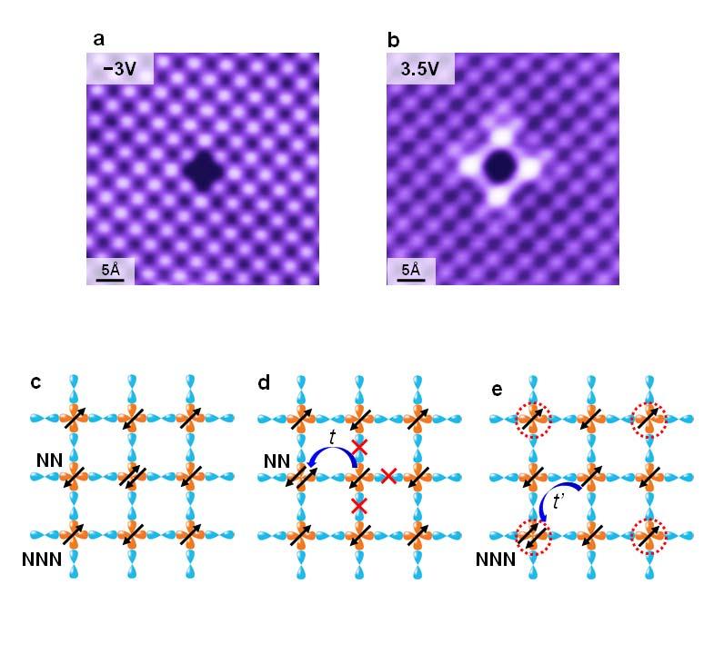
6 investigate the electronic state created by a single added charge. For this purpose we take advantage of the missing Cl defect naturally occurred on cleaved CCOC surface. Since each Cl ion strongly grasps an extra electron, a missing Cl effectively donates an electron into the CuO 2 plane. The red curve in Fig. 2c shows the di/dv measured directly on the missing Cl site compared to that taken at a location far from the defect (black curve). The most dramatic spectroscopic feature caused by the doped electron is the emergence of a broad electronic state within the charge transfer gap near the edge of the UHB. Meanwhile, the peak of the UHB is completely suppressed, indicating the transfer of its spectral weight to the in-gap state. The CTB, in contrast, only shifts very slightly, indicating a strong particle-hole asymmetry induced by the doped electron. Moreover, the local charge transfer gap at the defect center is substantially reduced to Δ = 1.6eV. The schematic electronic structure induced by the doped electron is drawn in Fig. 2d. The spatial distribution of the doped electronic state is another fundamental issue that STM is particularly suited for investigating. Figure 3a shows a series of di/dv spectra taken as the STM tip is positioned away from the defect center along the Cu-O bond direction (inset of Fig. 3a), which reveals the vanishing in-gap state accompanied by the emerging UHB peak. At a distance of six lattice constants from the defect center, the di/dv curve fully recovers that of the pristine Mott insulator. By subtracting this background from the di/dv curve at each location, the relative contribution of the defect state can be extracted. As shown in Fig. 3b, both the amplitude of the in-gap state and the suppression of UHB decrease systematically with increasing distance from the defect center. Figure 3c shows that the profile can be fit very well by using two Gaussian terms representing the created in-gap state and suppressed
7 UHB respectively (see Supplementary Information for details). The spectral weight of the in-gap state can be roughly estimated by the area enclosed by the Gaussian fit (Fig. S4). Figure 3d summarizes the spatial evolution of the spectral weight, which loses half of its strength within a distance of three lattice sites, or merely 12Å from the defect center. The in-gap state is thus strongly localized in space. High resolution topography near the defect reveals another interesting trend. Figure 4a shows the image taken at negative bias V s = -3.0V, which reflects the occupied state characteristics. Except for the dark pit at the missing Cl site, there is no other pronounced spatial pattern. Figure 4b displays the image taken at the same area with positive bias V s = 3.5V, which reflects the empty state characteristics. It shows a very dramatic spatial pattern where the four next-nearest-neighbor (NNN) sites appear to be anomalously bright. The strong bias dependence provides another piece of evidence for the particle-hole asymmetry where the CTB is insensitive to the doped electron but the UHB is strongly affected. Interestingly, similar features have been found at Ni impurities in superconducting Bi 2 Sr 2 CaCu 2 O 8+δ, where the NNN sites brighten up in the positive bias density of state map 11. However, the clear contrast reversal at negative bias observed there is absent in the present case. The properties of parent and lightly doped cuprates are crucial to the mechanism of high T C and have attracted tremendous theoretical interests 1. It was first proposed by Anderson that the essential physics is contained in the half-filled Hubbard model 2 :. H = t c c + U n n + iσ jσ i i i, j σ i
8 Here t is the hopping integral between nearest-neighbor (NN) sites and U is the onsite Coulomb repulsion. In the large U limit as in the cuprates, the Hubbard model is transformed into the t-j model, where J = 4t 2 /U is the superexchange energy. Since the two dimensional Hubbard or t-j models have yet to be solved exactly, various approximation schemes or numerical methods are employed to extract the effective low energy physics. The STM results shown above provide unprecedented real space information and full electronic spectrum that could help discriminate the different models. A major theoretical debate is whether a single band model is a valid low energy model for the cuprates 22. The charge transfer nature of the parent insulator suggests that a three band model involving two O bands and one Cu band might be more appropriate. However, it was proposed that the lowest hole-doped state, namely the CTB, can be represented by a single Zhang-Rice singlet (ZRS) band 23, in which the doped hole residing resonantly in the four planar O sites form a singlet with the central Cu 2+ ion. There are two specific predictions in the ZRS picture. First, the Mott insulator phase has particle-hole symmetry and second, the ZRS can move freely through the Cu 2+ lattice and thus should distribute uniformly in space. Our STM results show that indeed undoped CCOC has a nearly particle-hole symmetric and spatially uniform electronic structure, apparently supporting the single band ZRS model. More quantitatively, the bandwidth of the CTB and UHB estimated from the Gaussian fit is in the order of 3J (J = 0.13eV in cuprate), which is also close to the calculation based on the single band t-j model 24. The electronic state induced by a doped charge has also been investigated extensively by theory 25, but it is still under debate whether the main effect is the shift of E F or the emergence
9 of new states or both. Our STM results demonstrate that the doped electron induces an in-gap state near the upper gap edge with its spectral weight mainly transferred from the UHB. There is no significant change of the Fermi level position and the CTB has negligible contribution to the spectral weight transfer. This rather unusual scenario is unexpected for doped charge transfer insulators 26,27. We note that the electron donated by a surface defect as studied here may not be the ideal case of electron doping discussed by most theories due to the possible redistribution of charge on the surface, the change of local bonding situation, and the existence of a defect potential. Nevertheless, the local electronic structure of a surface electron-donor defect represents a well-defined problem that could be used for testing the validity of available theories for doped Mott insulators. The peculiar spatial pattern near the defect reveals that the distribution of the doped electronic state is intimately related to the AF spin background. Figure 4c displays the schematic spin structure of the CuO 2 plane, showing that the NN and NNN sites constitute two magnetic sublattices. Figure 4d shows that hopping of the added electron to NN site will induce parallel alignment of NN spins which is energetically costly. Electron hopping to the NNN sites, on the other hand, preserves the AF spin configuration and is energetically more favorable (Fig. 4e). The brightness of the NNN sites in the positive bias image may reflect the significance of NNN hopping of the added electron. Although this simple picture is conceptually appealing, we reemphasize that a realistic model for the spatial structures near the defect, including the bias-dependent images and localization of the in-gap state, should include the influence of the defect in a similar manner as the treatment of impurity-induced state in superconducting cuprates 28.
10 The overall STM results support the single band t-j model supplemented by the higher order hopping terms, which has been shown to capture the essential features of the ARPES and RIXS results 5,29. More importantly, the high-bias scanning tunneling spectroscopy covering both the filled and empty states represents a powerful method for mapping the local electronic evolution. Applying this technique to cuprates with increased bulk dopings may help elucidate how the Mottness physics eventually leads to high T C superconductivity. Method Summary Sample growth. The single crystals of Ca 2 CuO 2 Cl 2 (CCOC) are grown by the flux method as described elsewhere 30. The powders of CaO and CuCl 2 are mixed with a molar ratio of 2:1 and put into an alumina crucible. The mixed powder is heated at 1053K for 24 hours (hs) with intermediate grindings. After that, the CCOC precursor is heated to 1053K at a ramp rate of 60K/h and kept at this temperature for 5h. It is then heated to 1203K at a ramp rate of 60K/h and kept at that temperature for 10h. In the end it is cooled down to room temperature at a ramp rate of 60K/h. Single crystals with typical size of 2mm 2mm 0.1mm can be harvested by cleaving the as-grown bulks. STM measurements. The STM experiments are performed with a cryogenic variable temperature ultrahigh vacuum STM system. The CCOC crystal is cleaved in situ at T = 77K and then transferred immediately into the STM sample stage. To make tunneling into the insulating CCOC possible, the STM experiments have to be performed at relative high temperature so that the sample has finite conductivity. At T = 5K the STM tip will crash into
11 the sample because the sample is so insulating that no tunneling current can be detected. Therefore all STM results reported in this paper are acquired at T = 77K. In addition to that, the sample bias voltage has to be set beyond the charge transfer gap so that there is finite density of state in the sample. Moreover, a small tunneling current is used because otherwise the tip-sample junction will be quite unstable under large biases at T = 77K. The typical setup parameters are sample bias V s = ±3V and tunneling current I t = 2-10pA. The STM topography is taken in the constant current mode, and the di/dv spectra on CCOC are collected using a standard lock-in technique with modulation frequency f = 423Hz.
12 References: 1 Lee, P. A., Nagaosa, N. & Wen, X.-G. Doping a Mott insulator: Physics of high-temperature superconductivity. Rev. Mod. Phys. 78, (2006). 2 Anderson, P. W. The Resonating Valence Bond State in La 2 CuO 4 and Superconductivity. Science 235, (1987). 3 Kastner, M. A., Birgeneau, R. J., Shirane, G. & Endoh, Y. Magnetic, transport, and optical properties of monolayer copper oxides. Rev. Mod. Phys. 70, (1998). 4 Abbamonte, P. et al. Resonant Inelastic X-Ray Scattering from Valence Excitations in Insulating Copper Oxides. Phys. Rev. Lett. 83, (1999). 5 Hasan, M. Z. et al. Electronic Structure of Mott Insulators Studied by Inelastic X-ray Scattering. Science 288, (2000). 6 Kim, Y. J. et al. Resonant Inelastic X-Ray Scattering Study of Charge Excitations in La 2 CuO 4. Phys. Rev. Lett. 89, (2002). 7 Wells, B. O. et al. E versus k Relations and Many Body Effects in the Model Insulating Copper Oxide Sr 2 CuO 2 Cl 2. Phys. Rev. Lett. 74, (1995). 8 Pothuizen, J. J. M. et al. Single Hole Dynamics in the CuO 2 Plane at Half Filling. Phys. Rev. Lett. 78, (1997). 9 Ronning, F. et al. Photoemission Evidence for a Remnant Fermi Surface and a d-wave-like Dispersion in Insulating Ca 2 CuO 2 Cl 2. Science 282, (1998). 10 Pan, S. H. et al. Imaging the effects of individual zinc impurity atoms on superconductivity in Bi 2 Sr 2 CaCu 2O8+δ. Nature 403, (2000). 11 Hudson, E. W. et al. Interplay of magnetism and high-tc superconductivity at individual Ni impurity atoms in Bi 2 Sr 2 CaCu 2 O 8+δ. Nature 411, (2001). 12 Hoffman, J. E. et al. A Four Unit Cell Periodic Pattern of Quasi-Particle States Surrounding Vortex Cores in Bi 2 Sr 2 CaCu 2 O 8+δ. Science 295, (2002). 13 Howald, C., Eisaki, H., Kaneko, N., Greven, M. & Kapitulnik, A. Periodic density-of-states modulations in superconducting Bi 2 Sr 2 CaCu 2 O 8+δ. Phys. Rev. B 67, (2003). 14 Hanaguri, T. et al. A 'checkerboard' electronic crystal state in lightly hole-doped Ca 2-x Na x CuO 2 Cl 2. Nature 430, (2004). 15 Vershinin, M. et al. Local Ordering in the Pseudogap State of the High-Tc Superconductor Bi 2 Sr 2 CaCu 2 O 8+δ. Science 303, (2004). 16 Gomes, K. K. et al. Visualizing pair formation on the atomic scale in the high-tc superconductor Bi 2 Sr 2 CaCu 2 O 8+δ. Nature 447, (2007). 17 Lee, J. et al. Spectroscopic Fingerprint of Phase-Incoherent Superconductivity in the Underdoped Bi 2 Sr 2 CaCu 2 O 8+δ. Science 325, (2009). 18 Hoffman, J. E. et al. Imaging Quasiparticle Interference in Bi 2 Sr 2 CaCu 2 O 8+δ. Science 297, (2002). 19 Shen, K. M. et al. Missing Quasiparticles and the Chemical Potential Puzzle in the Doping Evolution of the Cuprate Superconductors. Phys. Rev. Lett. 93, (2004). 20 Zaanen, J., Sawatzky, G. A. & Allen, J. W. Band gaps and electronic structure of transition-metal compounds. Phys. Rev. Lett. 55, (1985). 21 Lau, B., Berciu, M. & Sawatzky, G. A. High-Spin Polaron in Lightly Doped CuO 2 Planes. Phys. Rev.
13 Lett. 106, (2011). 22 Phillips, P. & Jarrell, M. Comment on X-ray Absorption Spectra Reveal the Inapplicability of the Single-Band Hubbard Model to Overdoped Cuprate Superconductors. Phys. Rev. Lett. 105, (2010). 23 Zhang, F. C. & Rice, T. M. Effective Hamiltonian for the superconducting Cu oxides. Phys. Rev. B 37, (1988). 24 Liu, Z. & Manousakis, E. Dynamical properties of a hole in a Heisenberg antiferromagnet. Phys. Rev. B 45, (1992). 25 Phillips, P. Colloquium: Identifying the propagating charge modes in doped Mott insulators. Rev. Mod. Phys. 82, (2010). 26 Meinders, M. B. J., Eskes, H. & Sawatzky, G. A. Spectral-weight transfer: Breakdown of low-energy-scale sum rules in correlated systems. Phys. Rev. B 48, (1993). 27 Kusunose, H. & Rice, T. M. Single-Particle Spectrum in the Electron-Doped Cuprates. Phys. Rev. Lett. 91, (2003). 28 Balatsky, A. V., Vekhter, I. & Zhu, J.-X. Impurity-induced states in conventional and unconventional superconductors. Rev. Mod. Phys. 78, (2006). 29 Kim, C. et al. Systematics of the Photoemission Spectral Function of Cuprates: Insulators and Holeand Electron-Doped Superconductors. Phys. Rev. Lett. 80, (1998). 30 Hiroi, Z., Kobayashi, N. & Takano, M. Probable hole-doped superconductivity without apical oxygens in (Ca, Na) 2 CuO 2 Cl 2. Nature 371, (1994). Supplementary information: A supplementary information session is available. Acknowledgments We thank Z. Y. Weng, T. Xiang, F. C. Zhang, and G. M. Zhang for helpful discussions. This work is supported by the NSF of China and by the MOST of China (Grants No. 2009CB and No. 2010CB923003). Author Information Correspondence and requests for materials should be addressed to Y.W. (yayuwang@tsinghua.edu.cn).
14 Figure Captions: Figure 1 Crystal structure and STM topography on CCOC. a, Crystal structure of Ca 2 CuO 2 Cl 2, which is similar to that of La 2 CuO 4 except that the LaO layer is replaced by CaCl layer. The crystal cleaves easily between two adjacent CaCl layers, as indicated by the gray planes, exposing the square lattice of Cl atoms. b, Constant current topographic image of CCOC taken at bias voltage V s = -3.5V and tunneling current I t = 10pA. Each cross-shaped dark site on the surface corresponds to a missing Cl defect most likely induced by the cleaving process. Figure 2 Spectroscopy on pure CCOC and the missing Cl defect. a, Spatially averaged di/dv spectrum over a defect-free area of CCOC reveals the full electronic structure across the Mott gap. (Inset) High-resolution image of the area where the spectra are taken. b, Schematic band structure of the pristine Mott insulator showing the upper Hubbard band (unfilled), the charge transfer band (pink) and the non bonding O 2p π band (green). c, The red curve shows the di/dv spectrum measured at the missing Cl defect center and the black curve is taken at a location far from the defect. (Inset) High-resolution image around a missing Cl defect and the red dot indicates where the red curve is taken. d, Schematic electronic structure at the defect center: an in-gap state (blue) emerges near the edge of UHB due to spectral weight transfer from the latter. The CTB is slightly shifted and the local gap amplitude is significantly reduced. Figure 3 Spatial distribution of the doped electronic state. a, A series of di/dv spectra taken at locations away from the defect center along the Cu-O bond direction, as indicated in the inset by colored dots. b, Contribution of the doped electronic state to local electronic structure obtained by subtracting the background di/dv (obtained at six lattice distances away from the defect) from each di/dv spectrum in a. c, The di/dv curves in b can be fit well by two Gaussian terms and the spectral weight of the in-gap state can be estimated by the area enclosed by the Gaussian lineshape. d, Spatial dependence of the in-gap state spectral weight,
15 which decays rapidly with increasing lateral distance from the defect center. Figure 4 Bias dependent images around the defect. a and b, Constant current images around a missing Cl defect taken at negative and positive biases respectively. The positive bias image shows four bright spots at the NNN sites of the defect. c to e, Schematic illustration of the spin structure of the Mott insulator and how an added electron hops in the presence of an AF spin background. Hopping to the NN site (t) disturbs the original AF spin configuration (the red cross indicates the parallel alignment of NN spins), whereas hopping to the NNN sites (t ) has no spin consequence.

16 Figure 1
17 Figure 2
18 Figure 3
19 Figure 4
20 Supplementary information for Visualizing the atomic scale electronic structure of the Ca 2 CuO 2 Cl 2 Mott insulator Cun Ye 1,*, Peng Cai 1,*, Runze Yu 2, Xiaodong Zhou 1, Wei Ruan 1, Qingqing Liu 2, Changqing Jin 2 & Yayu Wang 1, 1 State Key Laboratory of Low Dimensional Quantum Physics, Department of Physics, Tsinghua University, Beijing , China 2 Institute of Physics, Chinese Academy of Sciences, Beijing , China * These authors contributed equally to this work. yayuwang@tsinghua.edu.cn Contents: SIA: Preparation and calibration of the STM tip SIB: Gaussian fit to the di/dv spectra of the CTB and UHB SIC: Atomically resolved electronic structure on pure CCOC SID: Fitting of the in-gap state spectra Figure S1 to S4 References

21 SIA: Preparation and calibration of the STM tip The STM tip condition is of particular concern when addressing the high-energy spectroscopic features. Not only has it to be stable under high biases, but also its electronic DOS should be relatively featureless over a wide energy window. We have developed a routine for STM tip treatment and calibration. We use electro-chemically etched polycrystalline tungsten tip for all the measurement. Before the STM experiments on CCOC, the tip is first treated by in situ high voltage e-beam sputtering, which is very efficient for cleaning and sharpening the tip. We then use the tip to approach an atomically clean crystalline Au(111) surface prepared in situ by repeated Ne ion sputtering and high temperature annealing. By taking topographic scans and spectroscopic measurements on clean Au(111) surface, we could check if the tip shape or spectrum is ideal. If necessary further tip treatment can be done by field emission process or controlled gentle crash into the Au(111) crystal. Fig.S1. a, Constant-current STM image of Au(111) surface (V s = 0.1V, I t = 0.1nA), which shows clearly the herringbone reconstruction. The standing wave patterns near the defect are also visible. b, Typical di/dv spectrum measured with an clean tungsten tip on Au(111) surface, which shows no distinctive feature except the surface state band setting in around V s = 0.5V Fig. S1a shows a typical constant-current image on Au(111) surface taken with V s = 0.1V
22 and I t = 0.1nA, which shows clear herringbone reconstruction, standing waves patterns induced by the quasiparticle interference of the surface state, and nearly circular shaped defects. Fig. S1b displays the di/dv spectroscopy over a wide range of sample bias from -2.5V to 3.5V. The abrupt jump at V s ~ 0.5V is due to the onset of the surface state band of the Au(111) surface 1. The steep increase of di/dv at large negative bias is due to the Au bulk electronic states. There is no spurious electronic state within the energy range of interest that may be induced by unwanted adsorbates on the tip. Both the topography and spectroscopy indicate that the tip is clean and stable. High quality large-bias, high temperature STM results can usually be obtained with such a tungsten tip. SIB: Gaussian fit to the di/dv spectra of the CTB and UHB In previous ARPES studies on CCOC, it was found that the energy distribution curve (EDC) along a specific momentum (k) of the charge transfer (CTB) or Zhang-Rice singlet (ZRS) band can be fit by a broad Gaussian lineshape rather than a sharp Lorentzian lineshape for well-defined quasiparticles (qps). Moreover, the width of the EDC is comparable to the entire bandwidth determined by the dispersion of the band 2. These observations have been interpreted as evidence for the breakdown of the coherent qp picture in the Mott insulators. Unlike the k-resolved EDC curve measured by ARPES, the di/dv curves measured by STM are related to the k-integrated spectral function. Interestingly, we find that the di/dv curves of the CTB and the upper Hubbard band (UHB) on CCOC shown in the main text can also be fit by Gaussian lineshape. Fig. S2a shows the zoom-in di/dv curve of the CTB, which shows that the low energy half of the curve can be fit very well with a Gaussian lineshape. For the high energy half, the fitting is spoiled by the rapid increase of di/dv due to the onset of the nonbonding oxygen states. The width of CTB, estimated to be 0.47eV from the full width at half maximum (FWHM) of the Gaussian fit, is in rough agreement with the bandwidth (W = 0.35eV) determined by ARPES. The situation of the UHB, which cannot be detected by ARPES, is quite similar. Fig. S2b shows the di/dv curve of the UHB, which can also be fit very well by the Gaussian lineshape with a FWHM of 0.34eV. Both the band width of the
23 CTB and UHB thus is in the order of 3J (J = 0.13eV in the cuprates), the calculated band width of the parent cuprate based on the single band t-j model 3. Fig.S2. The di/dv spectroscopy of the CTB (a) and UHB (b) of undoped CCOC. The red curves indicate Gaussian fits to the data. SIC: Atomically resolved electronic structure on pure CCOC The real space electronic characteristics are of great importance to Mott insulators, where local Coulomb repulsion plays a dominant role. STM is arguably the most ideal experimental technique for addressing this issue. Fig. S3 displays spatially resolved di/dv spectra taken at three different atomic sites, as marked in the inset. The black, red and blue curves depict the spectra taken on Cu, O and Ca sites, respectively. The setup conditions are V S = 3V and I t = 10pA. The curves are barely distinguishable on the negative bias side. In particular, the CTB possesses exactly the same peak shape and intensity on these 3 sites. On the positive bias side, the intensity of UHB is slightly suppressed on Ca site compared to those on Cu and O sites. However, the difference is rather small and varies slightly from different experimental runs.
24 Therefore we could conclude that there is no significant difference between the electronic structures on different lattice sites. Both the CTB and UHB are uniformly distributed in space. Fig.S3. di/dv spectra taken on the Cu, Ca and O sites of the CCOC surface, as indicated in the inset. There is no significant difference between the spectra, demonstrating spatially uniform electronic structures. SID: Fitting of the in-gap state spectra
25 a 0.1 b 0.1 di/dv (a.u.) di/dv (a.u.) sample bias (V) sample bias (V) c 0.10 d di/dv (a.u.) di/dv (a.u.) sample bias (V) sample bias (V) e 0.04 f di/dv (a.u.) di/dv (a.u.) sample bias (V) sample bias (V) Fig.S4. (a to f) di/dv spectra taken at locations away from the missing-cl along the Cu-O bond direction with the background subtracted. The green curves show the two Gaussian curves for the in-gap state and the suppression of UHB respectively, and red curves show the summation of the two terms.
26 Fig. 3a in the main text displays the electronic structure measured at different locations near the missing Cl defect, which demonstrates the spatial decay. By subtracting di/dv curve of pristine CCOC from spectrum measured around the defect (Fig. 3b), the relative contribution of the defect state and the suppression of UHB can be extracted. We find that the subtracted curves can be fit very well with the following formula: ( ) 2 A i x x y = exp i ci 2 πσ σ = 1, 2 i i Here the summation includes the two Gaussian terms representing the created in-gap state and the suppression of UHB. A i corresponds to the area enclosed by each curve, x ci is the peak position and σ i = Γ i / 4ln 2 where Г i is the FWHM of the Gaussian fit. The green solid curves in Fig. S4 (a to f) indicate the two Gaussian curves while the red curves show the combination of the two terms. The agreement between the fit and the data is very impressive. The in-gap state spectral weight plotted in Fig. 3d of the main text is the A 1 value, i.e., the area enclosed by the Gaussian fit for the created in-gap state. References: 1 Crommie, M. F., Lutz, C. P. & Eigler, D. M. Imaging standing waves in a two-dimensional electron gas. Nature 363, (1993). 2 Shen, K. M. et al. Missing Quasiparticles and the Chemical Potential Puzzle in the Doping Evolution of the Cuprate Superconductors. Phys. Rev. Lett. 93, (2004). 3 Liu, Z. & Manousakis, E. Dynamical properties of a hole in a Heisenberg antiferromagnet. Phys. Rev. B 45, (1992).
Visualizing the evolution from the Mott insulator to a charge-ordered insulator in lightly doped cuprates
 Visualizing the evolution from the Mott insulator to a charge-ordered insulator in lightly doped cuprates Peng Cai 1, Wei Ruan 1, Yingying Peng, Cun Ye 1, Xintong Li 1, Zhenqi Hao 1, Xingjiang Zhou,5,
Visualizing the evolution from the Mott insulator to a charge. ordered insulator in lightly doped cuprates
 Visualizing the evolution from the Mott insulator to a charge ordered insulator in lightly doped cuprates Peng Cai, 1 Wei Ruan, 1 Yingying Peng, 2 Cun Ye, 1 Xintong Li, 1 Zhenqi Hao, 1 Xingjiang Zhou,
Relationship between the parent charge transfer gap and maximum transition temperature in cuprates
 Sci. Bull. (6) 6():86 8 DOI.7/s-6--x Article www.scibull.com www.springer.com/scp Physics & Astronomy Relationship between the parent charge transfer gap and maximum transition temperature in cuprates
arxiv: v1 [cond-mat.supr-con] 28 May 2018
![arxiv: v1 [cond-mat.supr-con] 28 May 2018](/thumbs/91/107009379.jpg "arxiv: v1 [cond-mat.supr-con] 28 May 2018") Evidence for Multiple Underlying Fermi Surface and Isotropic Energy Gap in the Cuprate Parent Compound Ca 2 CuO 2 Cl 2 Cheng Hu 1,2, Jian-Fa Zhao 1,2, Ying Ding 1,2, Jing Liu 1,2, Qiang arxiv:1805.10991v1
Evidence for Multiple Underlying Fermi Surface and Isotropic Energy Gap in the Cuprate Parent Compound Ca 2 CuO 2 Cl 2 Cheng Hu 1,2, Jian-Fa Zhao 1,2, Ying Ding 1,2, Jing Liu 1,2, Qiang arxiv:1805.10991v1
High-T c superconductors. Parent insulators Carrier doping Band structure and Fermi surface Pseudogap and superconducting gap Transport properties
 High-T c superconductors Parent insulators Carrier doping Band structure and Fermi surface Pseudogap and superconducting gap Transport properties High-T c superconductors Parent insulators Phase diagram
The Hubbard model in cold atoms and in the high-tc cuprates
 The Hubbard model in cold atoms and in the high-tc cuprates Daniel E. Sheehy Aspen, June 2009 Sheehy@LSU.EDU What are the key outstanding problems from condensed matter physics which ultracold atoms and
SUPPLEMENTARY INFORMATION
 doi: 10.1038/nature06219 SUPPLEMENTARY INFORMATION Abrupt Onset of Second Energy Gap at Superconducting Transition of Underdoped Bi2212 Wei-Sheng Lee 1, I. M. Vishik 1, K. Tanaka 1,2, D. H. Lu 1, T. Sasagawa
Tuning order in cuprate superconductors
 Tuning order in cuprate superconductors arxiv:cond-mat/0201401 v1 23 Jan 2002 Subir Sachdev 1 and Shou-Cheng Zhang 2 1 Department of Physics, Yale University, P.O. Box 208120, New Haven, CT 06520-8120,
arxiv:cond-mat/ v3 [cond-mat.supr-con] 23 May 2000
![arxiv:cond-mat/ v3 [cond-mat.supr-con] 23 May 2000](/thumbs/75/71950529.jpg "arxiv:cond-mat/ v3 [cond-mat.supr-con] 23 May 2000") Electronic Structure of La 2 x Sr x CuO 4 in the Vicinity of the Superconductor-Insulator Transition arxiv:cond-mat/99248v3 [cond-mat.supr-con] 23 May 2 A. Ino, C. Kim 2, M. Nakamura 3, T. Yoshida, T.
Electronic Structure of La 2 x Sr x CuO 4 in the Vicinity of the Superconductor-Insulator Transition arxiv:cond-mat/99248v3 [cond-mat.supr-con] 23 May 2 A. Ino, C. Kim 2, M. Nakamura 3, T. Yoshida, T.
Quantum dynamics in many body systems
 Quantum dynamics in many body systems Eugene Demler Harvard University Collaborators: David Benjamin (Harvard), Israel Klich (U. Virginia), D. Abanin (Perimeter), K. Agarwal (Harvard), E. Dalla Torre (Harvard)
Angle-Resolved Two-Photon Photoemission of Mott Insulator
 Angle-Resolved Two-Photon Photoemission of Mott Insulator Takami Tohyama Institute for Materials Research (IMR) Tohoku University, Sendai Collaborators IMR: H. Onodera, K. Tsutsui, S. Maekawa H. Onodera
Phase Separation and Magnetic Order in K-doped Iron Selenide Superconductor
 Phase Separation and Magnetic Order in K-doped Iron Selenide Superconductor Wei Li 1, Hao Ding 1, Peng Deng 1, Kai Chang 1, Canli Song 1, Ke He 2, Lili Wang 2, Xucun Ma 2, Jiang-Ping Hu 3, Xi Chen 1, *,
High-T c superconductors
 High-T c superconductors Parent insulators Carrier doping Band structure and Fermi surface Pseudogap, superconducting gap, superfluid Nodal states Bilayer, trilayer Stripes High-T c superconductors Parent
Direct Observation of Nodes and Twofold Symmetry in FeSe Superconductor
 www.sciencemag.org/cgi/content/full/332/6036/1410/dc1 Supporting Online Material for Direct Observation of Nodes and Twofold Symmetry in FeSe Superconductor Can-Li Song, Yi-Lin Wang, Peng Cheng, Ye-Ping
Vortex Checkerboard. Chapter Low-T c and Cuprate Vortex Phenomenology
 63 Chapter 4 Vortex Checkerboard There is no need to invoke alternative order parameters to explain observed DOS modulations in optimally doped Bi 2 Sr 2 CaCu 2 O 8+δ. To continue the search for interesting
Twenty years have passed since the discovery of the first copper-oxide high-temperature superconductor
 1 Chapter 1 Introduction Twenty years have passed since the discovery of the first copper-oxide high-temperature superconductor La 2 x Ba x CuO 4 in 1986, and the intriguing physics of cuprate superconductors
Studies of Iron-Based Superconductor Thin Films
 MBE Growth and STM Studies of Iron-Based Superconductor Thin Films Wei Li 1, Canli Song 1,2, Xucun Ma 2, Xi Chen 1*, Qi-Kun Xu 1 State Key Laboratory of Low-Dimensional Quantum Physics, Department of Physics,
Polaronic Effects in the Lightly Doped Cuprates. Kyle M. Shen Stanford University
 Polaronic Effects in the Lightly Doped Cuprates Kyle M. Shen Stanford University April 6, 2005 ARPES Studies of the Cuprates Temperature (K) AFI Bi 2 Sr 2 CaCu 2 O 8+δ Bi 2 Sr 2 CuO 6+δ YBa 2 Cu 3 O 7-δ
2) Atom manipulation. Xe / Ni(110) Model: Experiment:
 Atom manipulation. Xe / Ni(110) Model: Experiment:") 2) Atom manipulation D. Eigler & E. Schweizer, Nature 344, 524 (1990) Xe / Ni(110) Model: Experiment: G.Meyer, et al. Applied Physics A 68, 125 (1999) First the tip is approached close to the adsorbate
2) Atom manipulation D. Eigler & E. Schweizer, Nature 344, 524 (1990) Xe / Ni(110) Model: Experiment: G.Meyer, et al. Applied Physics A 68, 125 (1999) First the tip is approached close to the adsorbate
The Chemical Control of Superconductivity in Bi 2 Sr 2 (Ca 1 x Y x )Cu 2 O 8+±
Cu 2 O 8+±") CHINESE JOURNAL OF PHYSICS VOL. 38, NO. 2-II APRIL 2000 The Chemical Control of Superconductivity in Bi 2 Sr 2 (Ca 1 x Y x )Cu 2 O 8+± R. S. Liu 1, I. J. Hsu 1, J. M. Chen 2, and R. G. Liu 2 1 Department
CHINESE JOURNAL OF PHYSICS VOL. 38, NO. 2-II APRIL 2000 The Chemical Control of Superconductivity in Bi 2 Sr 2 (Ca 1 x Y x )Cu 2 O 8+± R. S. Liu 1, I. J. Hsu 1, J. M. Chen 2, and R. G. Liu 2 1 Department
SUPPLEMENTARY INFORMATION
 DOI: 10.1038/NCHEM.2491 Experimental Realization of Two-dimensional Boron Sheets Baojie Feng 1, Jin Zhang 1, Qing Zhong 1, Wenbin Li 1, Shuai Li 1, Hui Li 1, Peng Cheng 1, Sheng Meng 1,2, Lan Chen 1 and
What's so unusual about high temperature superconductors? UBC 2005
 What's so unusual about high temperature superconductors? UBC 2005 Everything... 1. Normal State - doped Mott insulator 2. Pairing Symmetry - d-wave 2. Short Coherence Length - superconducting fluctuations
Quasiparticle dynamics and interactions in non uniformly polarizable solids
 Quasiparticle dynamics and interactions in non uniformly polarizable solids Mona Berciu University of British Columbia à beautiful physics that George Sawatzky has been pursuing for a long time à today,
How to model holes doped into a cuprate layer
 How to model holes doped into a cuprate layer Mona Berciu University of British Columbia With: George Sawatzky and Bayo Lau Hadi Ebrahimnejad, Mirko Moller, and Clemens Adolphs Stewart Blusson Institute
SUPPLEMENTARY INFORMATION
 A Stable Three-dimensional Topological Dirac Semimetal Cd 3 As 2 Z. K. Liu, J. Jiang, B. Zhou, Z. J. Wang, Y. Zhang, H. M. Weng, D. Prabhakaran, S. -K. Mo, H. Peng, P. Dudin, T. Kim, M. Hoesch, Z. Fang,
A momentum-dependent perspective on quasiparticle interference in Bi 2 Sr 2 CaCu 2 O 8+δ
 SLAC-PUB-14004 A momentum-dependent perspective on quasiparticle interference in Bi 2 Sr 2 CaCu 2 O 8+δ I. M. Vishik, 1,2 B. Moritz, 2 E. A. Nowadnick, 1,2 W. S. Lee, 1,2 K. Tanaka, 3 T. Sasagawa, 4 T.
Key words: High Temperature Superconductors, ARPES, coherent quasiparticle, incoherent quasiparticle, isotope substitution.
 Lattice Dynamics and Electron Pairing in High Temperature Superconductors A. Lanzara 1,2, G.-H. Gweon 3, S. Y. Zhou 1 1 Department of Physics, University of California, Berkeley, CA 94720, U.S.A. 2 Materials
Spatially resolving density-dependent screening around a single charged atom in graphene
 Supplementary Information for Spatially resolving density-dependent screening around a single charged atom in graphene Dillon Wong, Fabiano Corsetti, Yang Wang, Victor W. Brar, Hsin-Zon Tsai, Qiong Wu,
Time-Resolved and Momentum-Resolved Resonant Soft X-ray Scattering on Strongly Correlated Systems
 Time-Resolved and Momentum-Resolved Resonant Soft X-ray Scattering on Strongly Correlated Systems Wei-Sheng Lee Stanford Institute of Material and Energy Science (SIMES) SLAC & Stanford University Collaborators
Lattice modulation experiments with fermions in optical lattices and more
 Lattice modulation experiments with fermions in optical lattices and more Nonequilibrium dynamics of Hubbard model Ehud Altman Weizmann Institute David Pekker Harvard University Rajdeep Sensarma Harvard
Inelastic light scattering and the correlated metal-insulator transition
 Inelastic light scattering and the correlated metal-insulator transition Jim Freericks (Georgetown University) Tom Devereaux (University of Waterloo) Ralf Bulla (University of Augsburg) Funding: National
arxiv:cond-mat/ v1 [cond-mat.supr-con] 28 May 2003
![arxiv:cond-mat/ v1 [cond-mat.supr-con] 28 May 2003](/thumbs/96/128981112.jpg "arxiv:cond-mat/ v1 [cond-mat.supr-con] 28 May 2003") arxiv:cond-mat/0305637v1 [cond-mat.supr-con] 28 May 2003 The superconducting state in a single CuO 2 layer: Experimental findings and scenario Rushan Han, Wei Guo School of Physics, Peking University,
arxiv:cond-mat/0305637v1 [cond-mat.supr-con] 28 May 2003 The superconducting state in a single CuO 2 layer: Experimental findings and scenario Rushan Han, Wei Guo School of Physics, Peking University,
Dynamics of fluctuations in high temperature superconductors far from equilibrium. L. Perfetti, Laboratoire des Solides Irradiés, Ecole Polytechnique
 Dynamics of fluctuations in high temperature superconductors far from equilibrium L. Perfetti, Laboratoire des Solides Irradiés, Ecole Polytechnique Superconductors display amazing properties: Dissipation-less
STM studies of impurity and defect states on the surface of the Topological-
 STM studies of impurity and defect states on the surface of the Topological- Insulators Bi 2 Te 3 and Bi 2 Se 3 Aharon Kapitulnik STANFORD UNIVERSITY Zhanybek Alpichshev Yulin Chen Jim Analytis J.-H. Chu
Spectroscopies for Unoccupied States = Electrons
 Spectroscopies for Unoccupied States = Electrons Photoemission 1 Hole Inverse Photoemission 1 Electron Tunneling Spectroscopy 1 Electron/Hole Emission 1 Hole Absorption Will be discussed with core levels
Probing the Electronic Structure of Complex Systems by State-of-the-Art ARPES Andrea Damascelli
 Probing the Electronic Structure of Complex Systems by State-of-the-Art ARPES Andrea Damascelli Department of Physics & Astronomy University of British Columbia Vancouver, B.C. Outline: Part I State-of-the-Art
Citation PHYSICAL REVIEW LETTERS (2000), 85( RightCopyright 2000 American Physical So
, 85( RightCopyright 2000 American Physical So") Title Discriminating the superconducting Bi2Sr2CaCu2O8+delta by interlayer t Author(s) Suzuki, M; Watanabe, T Citation PHYSICAL REVIEW LETTERS (2), 85( Issue Date 2-11-27 URL http://hdl.handle.net/2433/39919
Title Discriminating the superconducting Bi2Sr2CaCu2O8+delta by interlayer t Author(s) Suzuki, M; Watanabe, T Citation PHYSICAL REVIEW LETTERS (2), 85( Issue Date 2-11-27 URL http://hdl.handle.net/2433/39919
Supplementary figures
 Supplementary figures Supplementary Figure 1. A, Schematic of a Au/SRO113/SRO214 junction. A 15-nm thick SRO113 layer was etched along with 30-nm thick SRO214 substrate layer. To isolate the top Au electrodes
Topological edge states in a high-temperature superconductor FeSe/SrTiO 3 (001) film
 film") Topological edge states in a high-temperature superconductor FeSe/SrTiO 3 (001) film Z. F. Wang 1,2,3+, Huimin Zhang 2,4+, Defa Liu 5, Chong Liu 2, Chenjia Tang 2, Canli Song 2, Yong Zhong 2, Junping Peng
Topological edge states in a high-temperature superconductor FeSe/SrTiO 3 (001) film Z. F. Wang 1,2,3+, Huimin Zhang 2,4+, Defa Liu 5, Chong Liu 2, Chenjia Tang 2, Canli Song 2, Yong Zhong 2, Junping Peng
Dimensionality controlled Mott transition and correlation effects in
 Dimensionality controlled Mott transition and correlation effects in single- and bi-layer perovskite iridates Q. Wang, 1 Y. Cao, 1 J. A. Waugh, 1 S. R. Park, 1 T. F. Qi, 2 O. B. Korneta, 2 G. Cao, 2 and
Spin-Charge Separation in 1-D. Spin-Charge Separation in 1-D. Spin-Charge Separation - Experiment. Spin-Charge Separation - Experiment
 Spin-Charge Separation in 1-D Lecture: Solvable 1D electron systems, Mott insulator and correlated electron systems in 2D Solid State Spectroscopy Course 25/2/2013 Spin : J Charge : t Decay of a photohole
STM spectroscopy (STS)
") STM spectroscopy (STS) di dv 4 e ( E ev, r) ( E ) M S F T F Basic concepts of STS. With the feedback circuit open the variation of the tunneling current due to the application of a small oscillating voltage
STM spectroscopy (STS) di dv 4 e ( E ev, r) ( E ) M S F T F Basic concepts of STS. With the feedback circuit open the variation of the tunneling current due to the application of a small oscillating voltage
Tunneling Spectroscopy of PCCO
 Tunneling Spectroscopy of PCCO Neesha Anderson and Amlan Biswas Department of Physics, University of Florida, Gainesville, Florida Abstract A point-contact probe capable of operating down to temperatures
Scanning Tunneling Microscopy & Spectroscopy: A tool for probing electronic inhomogeneities in correlated systems
 Scanning Tunneling Microscopy & Spectroscopy: A tool for probing electronic inhomogeneities in correlated systems Anjan K. Gupta Physics Department, I. I. T Kanpur ICTS-GJ, IITK, Feb 2010 Acknowledgements
Observation of topological surface state quantum Hall effect in an intrinsic three-dimensional topological insulator
 Observation of topological surface state quantum Hall effect in an intrinsic three-dimensional topological insulator Authors: Yang Xu 1,2, Ireneusz Miotkowski 1, Chang Liu 3,4, Jifa Tian 1,2, Hyoungdo
SUPPLEMENTARY INFORMATION
 In the format provided by the authors and unedited. DOI: 10.1038/NPHYS4186 Stripes Developed at the Strong Limit of Nematicity in FeSe film Wei Li 1,2,3*, Yan Zhang 2,3,4,5, Peng Deng 1, Zhilin Xu 1, S.-K.
Cuprate high-t c superconductors
 Cuprate high-t c superconductors In solid-state physics two different paradigms are typically applied. The first is a local picture, in which one visualizes the quantum states of electrons in atomic orbitals
Photoelectron Interference Pattern (PEIP): A Two-particle Bragg-reflection Demonstration
: A Two-particle Bragg-reflection Demonstration") Photoelectron Interference Pattern (PEIP): A Two-particle Bragg-reflection Demonstration Application No. : 2990 Beamlime: BL25SU Project Leader: Martin Månsson 0017349 Team Members: Dr. Oscar Tjernberg
Photoelectron Interference Pattern (PEIP): A Two-particle Bragg-reflection Demonstration Application No. : 2990 Beamlime: BL25SU Project Leader: Martin Månsson 0017349 Team Members: Dr. Oscar Tjernberg
High temperature superconductivity
 High temperature superconductivity Applications to the maglev industry Elsa Abreu April 30, 2009 Outline Historical overview of superconductivity Copper oxide high temperature superconductors Angle Resolved
Name: (a) What core levels are responsible for the three photoelectron peaks in Fig. 1?
 What core levels are responsible for the three photoelectron peaks in Fig. 1?") Physics 243A--Surface Physics of Materials: Spectroscopy Final Examination December 16, 2014 (3 problems, 100 points total, open book, open notes and handouts) Name: [1] (50 points), including Figures
Physics 243A--Surface Physics of Materials: Spectroscopy Final Examination December 16, 2014 (3 problems, 100 points total, open book, open notes and handouts) Name: [1] (50 points), including Figures
Topological Surface States Protected From Backscattering by Chiral Spin Texture
 1 Topological Surface States Protected From Backscattering by Chiral Spin Texture Pedram Roushan 1, Jungpil Seo 1, Colin V. Parker 1, Y. S. Hor 2, D. Hsieh 1, Dong Qian 1, Anthony Richardella 1, M. Z.
Strong spin triplet contribution of the first removal state in the insulating regime of
 Strong spin triplet contribution of the first removal state in the insulating regime of Bi 2Sr2Ca1 x YxCu 2O8+δ C.Janowitz 1 ), U. Seidel 1 ), R.-ST. Unger 1 ), A. Krapf 1 ), R.Manzke 1 ), V.A.Gavrichkov
Application of single crystalline tungsten for fabrication of high resolution STM probes with controlled structure 1
 Application of single crystalline tungsten for fabrication of high resolution STM probes with controlled structure 1 A. N. Chaika a, S. S. Nazin a, V. N. Semenov a, V. G. Glebovskiy a, S. I. Bozhko a,b,
Supporting Information
 Supporting Information Spatially-resolved imaging on photocarrier generations and band alignments at perovskite/pbi2 hetero-interfaces of perovskite solar cells by light-modulated scanning tunneling microscopy
Phases of Na x CoO 2
 Phases of Na x CoO 2 by Aakash Pushp (pushp@uiuc.edu) Abstract This paper deals with the various phases of Na x CoO 2 ranging from charge ordered insulator to Curie-Weiss metal to superconductor as the
Quantum theory of vortices in d-wave superconductors
 Quantum theory of vortices in d-wave superconductors Physical Review B 71, 144508 and 144509 (2005), Annals of Physics 321, 1528 (2006), Physical Review B 73, 134511 (2006), cond-mat/0606001. Leon Balents
Supplementary Figure 1 Experimental setup for crystal growth. Schematic drawing of the experimental setup for C 8 -BTBT crystal growth.
 Supplementary Figure 1 Experimental setup for crystal growth. Schematic drawing of the experimental setup for C 8 -BTBT crystal growth. Supplementary Figure 2 AFM study of the C 8 -BTBT crystal growth
Electronic Noise Due to Thermal Stripe Switching
 Electronic Noise Due to Thermal Stripe Switching E. W. Carlson B. Phillabaum Y. L. Loh D. X. Yao Research Corporation Solid Liquid Gas www.stonecropgallery.com/artists/caleb/01-solidliquidgas.jpg Crystals
Scanning Tunneling Microscopy Studies of the Ge(111) Surface
 Surface") VC Scanning Tunneling Microscopy Studies of the Ge(111) Surface Anna Rosen University of California, Berkeley Advisor: Dr. Shirley Chiang University of California, Davis August 24, 2007 Abstract: This
VC Scanning Tunneling Microscopy Studies of the Ge(111) Surface Anna Rosen University of California, Berkeley Advisor: Dr. Shirley Chiang University of California, Davis August 24, 2007 Abstract: This
Origin of the anomalous low temperature upturn in resistivity in the electron-doped cuprates.
 Origin of the anomalous low temperature upturn in resistivity in the electron-doped cuprates. Y. Dagan 1, A. Biswas 2, M. C. Barr 1, W. M. Fisher 1, and R. L. Greene 1. 1 Center for Superconductivity Research,
Dual vortex theory of doped antiferromagnets
 Dual vortex theory of doped antiferromagnets Physical Review B 71, 144508 and 144509 (2005), cond-mat/0502002, cond-mat/0511298 Leon Balents (UCSB) Lorenz Bartosch (Harvard) Anton Burkov (Harvard) Predrag
Can superconductivity emerge out of a non Fermi liquid.
 Can superconductivity emerge out of a non Fermi liquid. Andrey Chubukov University of Wisconsin Washington University, January 29, 2003 Superconductivity Kamerling Onnes, 1911 Ideal diamagnetism High Tc
Order and quantum phase transitions in the cuprate superconductors
 Order and quantum phase transitions in the cuprate superconductors Subir Sachdev Department of Physics, Yale University, P.O. Box 208120, New Haven CT 06520-8120 March 26, 2003 Abstract This is a summary
Spin-orbital separation in the quasi-one-dimensional Mott insulator Sr 2 CuO 3 Splitting the electron
 Spin-orbital separation in the quasi-one-dimensional Mott insulator Sr 2 CuO 3 Splitting the electron James Gloudemans, Suraj Hegde, Ian Gilbert, and Gregory Hart December 7, 2012 The paper We describe
Supplementary Information
 Supplementary Information Supplementary Figures a b A B Supplementary Figure S1: No distortion observed in the graphite lattice. (a) Drift corrected and reorientated topographic STM image recorded at +300
YBCO. CuO 2. the CuO 2. planes is controlled. from deviation from. neutron. , blue star for. Hg12011 (this work) for T c = 72
 for T c = 72") Supplementary Figure 1 Crystal structures and joint phase diagram of Hg1201 and YBCO. (a) Hg1201 features tetragonal symmetry and one CuO 2 plane per primitive cell. In the superconducting (SC) doping
Supplementary Figure 1 Crystal structures and joint phase diagram of Hg1201 and YBCO. (a) Hg1201 features tetragonal symmetry and one CuO 2 plane per primitive cell. In the superconducting (SC) doping
Supplementary Materials for
 advances.sciencemag.org/cgi/content/full/4/9/eaat8355/dc1 Supplementary Materials for Electronic structures and unusually robust bandgap in an ultrahigh-mobility layered oxide semiconductor, Bi 2 O 2 Se
High Temperature Cuprate Superconductors
 High Temperature Cuprate Superconductors Theoretical Physics Year 4 Project T. K. Kingsman School of Physics and Astronomy University of Birmingham March 1, 2015 Outline 1 Introduction Cuprate Structure
Quantum Condensed Matter Physics Lecture 12
 Quantum Condensed Matter Physics Lecture 12 David Ritchie QCMP Lent/Easter 2016 http://www.sp.phy.cam.ac.uk/drp2/home 12.1 QCMP Course Contents 1. Classical models for electrons in solids 2. Sommerfeld
Mapping the electronic structure of each ingredient oxide layer of high T c cuprate superconductors
 IASTU Physics Seminar Mapping the electronic structure of each ingredient oxide layer of high T c cuprate superconductors Can-Li Song( 宋灿立 ) Department of Physics, Tsinghua University October 28, 2015
Tunable Dirac Fermion Dynamics in Topological Insulators
 Supplementary information for Tunable Dirac Fermion Dynamics in Topological Insulators Chaoyu Chen 1, Zhuojin Xie 1, Ya Feng 1, Hemian Yi 1, Aiji Liang 1, Shaolong He 1, Daixiang Mou 1, Junfeng He 1, Yingying
2.1 Experimental and theoretical studies
 Chapter 2 NiO As stated before, the first-row transition-metal oxides are among the most interesting series of materials, exhibiting wide variations in physical properties related to electronic structure.
Electronic structure of correlated electron systems. Lecture 2
 Electronic structure of correlated electron systems Lecture 2 Band Structure approach vs atomic Band structure Delocalized Bloch states Fill up states with electrons starting from the lowest energy No
Temperature-Dependent Angle-Resolved Photoemission Study of High-T c Superconductors
 Temperature-Dependent Angle-Resolved Photoemission Study of High-T c Superconductors Master Thesis Satoru Kudo Department of Complexity Science and Engineering, University of Tokyo February, 28 Contents
Curriculum Vitae December 2006
 Appendix: (A brief description of some representative results) (1) Electronic states of Pb adatom and Pb adatom chains on Pb(111) have been investigated by spatially scanning tunneling spectroscopy (STS)
Real Space Bogoliubov de Gennes Equations Study of the Boson Fermion Model
 Vol. 114 2008 ACTA PHYSICA POLONICA A No. 1 Proceedings of the XIII National School of Superconductivity, L adek Zdrój 2007 Real Space Bogoliubov de Gennes Equations Study of the Boson Fermion Model J.
Principles of Electron Tunneling Spectroscopy
 Principles of Electron Tunneling Spectroscopy Second Edition E. L. Wolf Polytechnic Institute of New York University, USA OXFORD UNIVERSITY PRESS Contents 1 Introduction 1.1 Concepts of quantum mechanical
Hole-concentration dependence of band structure in (Bi,Pb) 2 (Sr,La) 2 CuO 6+δ determined by the angle-resolved photoemission spectroscopy
 2 (Sr,La) 2 CuO 6+δ determined by the angle-resolved photoemission spectroscopy") Journal of Electron Spectroscopy and Related Phenomena 137 140 (2004) 663 668 Hole-concentration dependence of band structure in (Bi,Pb) 2 (Sr,La) 2 CuO 6+δ determined by the angle-resolved photoemission
Journal of Electron Spectroscopy and Related Phenomena 137 140 (2004) 663 668 Hole-concentration dependence of band structure in (Bi,Pb) 2 (Sr,La) 2 CuO 6+δ determined by the angle-resolved photoemission
8 Summary and outlook
 91 8 Summary and outlook The main task of present work was to investigate the growth, the atomic and the electronic structures of Co oxide as well as Mn oxide films on Ag(001) by means of STM/STS at LT
Talk online at
 Talk online at http://sachdev.physics.harvard.edu Outline 1. CFT3s in condensed matter physics Superfluid-insulator and Neel-valence bond solid transitions 2. Quantum-critical transport Collisionless-t0-hydrodynamic
SUPPLEMENTARY INFORMATION
 In the format provided by the authors and unedited. Intrinsically patterned two-dimensional materials for selective adsorption of molecules and nanoclusters X. Lin 1,, J. C. Lu 1,, Y. Shao 1,, Y. Y. Zhang
Magnetism and Superconductivity in Decorated Lattices
 Magnetism and Superconductivity in Decorated Lattices Mott Insulators and Antiferromagnetism- The Hubbard Hamiltonian Illustration: The Square Lattice Bipartite doesn t mean N A = N B : The Lieb Lattice
Magnetism in correlated-electron materials
 Magnetism in correlated-electron materials B. Keimer Max-Planck-Institute for Solid State Research focus on delocalized electrons in metals and superconductors localized electrons: Hinkov talk outline
Chapter 5 Nanomanipulation. Chapter 5 Nanomanipulation. 5.1: With a nanotube. Cutting a nanotube. Moving a nanotube
 Objective: learn about nano-manipulation techniques with a STM or an AFM. 5.1: With a nanotube Moving a nanotube Cutting a nanotube Images at large distance At small distance : push the NT Voltage pulse
2 B B D (E) Paramagnetic Susceptibility. m s probability. A) Bound Electrons in Atoms
 Paramagnetic Susceptibility. m s probability. A) Bound Electrons in Atoms") Paramagnetic Susceptibility A) Bound Electrons in Atoms m s probability B +½ p ½e x Curie Law: 1/T s=½ + B ½ p + ½e +x With increasing temperature T the alignment of the magnetic moments in a B field is
Paramagnetic Susceptibility A) Bound Electrons in Atoms m s probability B +½ p ½e x Curie Law: 1/T s=½ + B ½ p + ½e +x With increasing temperature T the alignment of the magnetic moments in a B field is
Supplementary Figures
 Supplementary Figures Supplementary Figure S1: Calculated band structure for slabs of (a) 14 blocks EuRh2Si2/Eu, (b) 10 blocks SrRh2Si2/Sr, (c) 8 blocks YbRh2Si2/Si, and (d) 14 blocks EuRh2Si2/Si slab;
Spectroscopy at nanometer scale
 Spectroscopy at nanometer scale 1. Physics of the spectroscopies 2. Spectroscopies for the bulk materials 3. Experimental setups for the spectroscopies 4. Physics and Chemistry of nanomaterials Various
Studying Metal to Insulator Transitions in Solids using Synchrotron Radiation-based Spectroscopies.
 PY482 Lecture. February 28 th, 2013 Studying Metal to Insulator Transitions in Solids using Synchrotron Radiation-based Spectroscopies. Kevin E. Smith Department of Physics Department of Chemistry Division
Tunneling Spectra of Hole-Doped YBa 2 Cu 3 O 6+δ
 67 Chapter 4 Tunneling Spectra of Hole-Doped YBa 2 Cu 3 O 6+δ 1 4.1 Introduction The proximity of cuprate superconductors to the Mott insulating phase gives rise to novel superconducting behavior enriched
Onset of the Meissner effect at 65 K in FeSe thin film grown on Nb doped SrTiO 3 substrate
 Onset of the Meissner effect at 65 K in FeSe thin film grown on Nb doped SrTiO 3 substrate Zuocheng Zhang 1,4*, Yihua Wang 2,3*, Qi Song 2,5*, Chang Liu 1,4, Rui Peng 2,5, K.A. Moler 3, Donglai Feng 2,5
Scanning Tunneling Spectroscopy Studies of High-Temperature Cuprate Superconductors
 Scanning Tunneling Spectroscopy Studies of High-Temperature Cuprate Superconductors Thesis by Ching-Tzu Chen In Partial Fulfillment of the Requirements for the Degree of Doctor of Philosophy California
Universal Features of the Mott-Metal Crossover in the Hole Doped J = 1/2 Insulator Sr 2 IrO 4
 Universal Features of the Mott-Metal Crossover in the Hole Doped J = 1/2 Insulator Sr 2 IrO 4 Umesh Kumar Yadav Centre for Condensed Matter Theory Department of Physics Indian Institute of Science August
File name: Supplementary Information Description: Supplementary Notes, Supplementary Figures and Supplementary References
 File name: Supplementary Information Description: Supplementary Notes, Supplementary Figures and Supplementary References File name: Peer Review File Description: Supplementary Note 1. CALCULATION OF THE
Angle-resolved photoemission spectroscopy (ARPES) Overview-Physics 250, UC Davis Inna Vishik
 Overview-Physics 250, UC Davis Inna Vishik") Angle-resolved photoemission spectroscopy (ARPES) Overview-Physics 250, UC Davis Inna Vishik Outline Review: momentum space and why we want to go there Looking at data: simple metal Formalism: 3 step model
Angle-resolved photoemission spectroscopy (ARPES) Overview-Physics 250, UC Davis Inna Vishik Outline Review: momentum space and why we want to go there Looking at data: simple metal Formalism: 3 step model
SUPPLEMENTARY INFORMATION
 Simultaneous and coordinated rotational switching of all molecular rotors in a network Y. Zhang, H. Kersell, R. Stefak, J. Echeverria, V. Iancu, U. G. E. Perera, Y. Li, A. Deshpande, K.-F. Braun, C. Joachim,
Fermi surface evolution in the antiferromagnetic state for the electron-doped t-t -t -J model
 Title Fermi surface evolution in the antiferromagnetic state for the electron-doped t-t -t -J model Author(s) Yuan, Q; Chen, Y; Lee, TK; Ting, CS Citation Physical Review B (Condensed Matter and Materials
ELEMENTARY BAND THEORY
 ELEMENTARY BAND THEORY PHYSICIST Solid state band Valence band, VB Conduction band, CB Fermi energy, E F Bloch orbital, delocalized n-doping p-doping Band gap, E g Direct band gap Indirect band gap Phonon
Material Science II. d Electron systems
 Material Science II. d Electron systems 1. Electronic structure of transition-metal ions (May 23) 2. Crystal structure and band structure (June 13) 3. Mott s (June 20) 4. Metal- transition (June 27) 5.
SUPPLEMENTARY INFORMATION
 A Dirac point insulator with topologically non-trivial surface states D. Hsieh, D. Qian, L. Wray, Y. Xia, Y.S. Hor, R.J. Cava, and M.Z. Hasan Topics: 1. Confirming the bulk nature of electronic bands by
Angle Resolved Photoemission Spectroscopy. Dan Dessau University of Colorado, Boulder
 Angle Resolved Photoemission Spectroscopy Dan Dessau University of Colorado, Boulder Dessau@Colorado.edu Photoemission Spectroscopy sample hn Energy High K.E. Low B.E. e - analyzer E F e- hν Density of