Nonlinear Time and Temperature Dependent Analysis of the Lead-Free Solder Sealing Ring of a Photonic Switch
|
|
|
- Philomena Poole
- 6 years ago
- Views:
Transcription
1 Nonlinear Time and Temperature Dependent Analysis of the Lead-Free Solder Sealing Ring of a Photonic Switch J. Lau, Z. Mei, S. Pang, C. Amsden, J. Rayner and S. Pan Agilent Technologies, Inc Stevens Creek Blvd. Santa Clara, CA 95052
2 PURPOSES To determine the thermal-fatigue life of the lead-free solder sealing ring of a photonic switch under shipping/storing/handling conditions. The 48wt%Sn-52wt%In and 100wt%In solders are assumed to obey the Garofalo-Arrhenius creep constitutive law. The creep responses such as the creep strain energy density range per cycle are determined. In order to determine the thermal-fatigue life of the solder sealing ring of the photonic switch, a relationship between the number of cycle-to-failure (N f ) and the strain energy density range per cycle is needed. Thus, isothermal fatigue tests of the solder sealing ring are performed. In order to increase the confidence of the finite element analysis procedures, material properties, and boundary conditions, some of the simulation results are compared with the experimental results measured by the Twyman-Green interferometry method.
3 CONTENTS (1) Introduction (2) Boundary-Value Problem (2a) Geometry (2b) Materials (2c) Loading Conditions (3) Nonlinear Analysis of the Photonic Switch (3a) Creep Hysteresis Loops (3b) Deflections (3c) Shear Stress Time-History (3d) Creep Shear Strain Time-History (3e) Creep Strain Energy Density Range (4) Isothermal Fatigue Tests and Results (4a) Sample Preparation (4b) Test Set-Up and Procedures (4c) Test Results (5) Thermal-Fatigue Life Prediction of the Sealing Ring (6) Deflection by Twyman-Green Interferometry Method (7) Summary

4

5
6 Agilent s All-Optical Switch A silica-based planar lightwave circuit (PLC) chip, which contains two intersecting arrays of waveguides, with trenches etched into each crosspoint. A silicon-based actuator chip, which contains a matching pattern of electrically addressed resistive elements. These two chips are hermetically sealed together with the 48Sn-52In solder ring. At the default state, the trenches, along with the rest of the sealed space between the silica and silicon chips, are filled with a liquid whose refractive index matches the waveguides and properties are suitable for bubble creation and control. Optical signals passing along any guide on the silica chip simply pass on through. However, by activating a resistive element on the silicon chip, a bubble can be created at that crosspoint, so that total internal reflection occurs at the side-wall of the corresponding trench, and switching is achieved.

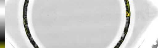
7 Sealing ring

8 1 Solder Sealing Ring Silica Chip Bolt Silicon Chip Aluminum Cooling Plate Molybdenum Substrate
9 Material Molybdenum (Mo) Young s Modulus (GPa) Poisson s Ratio Coefficient Of Thermal Expansion (ppm/ 0 C) Yield Strength (MPa) Tensile Strength (MPa) Elongation (%) Thermal Conductivity (W/m- 0 K) Density (g/cm 3 ) Specific Heat (cal/g- 0 K) 355 (1) 0.3 (7) 4.8 (1) 552 (1) 655 (1) 2.5 (3) 139 (1) (7) 0.06 (7) No Creep Silicon (Si) (1) 0.28 (1) 2.5 (1) 34.5 (1) 185 (1) (1) 2.4 (2) No 48Sn-52In 30.5 (8) 0.36 (8) 28 (1) 7.3 (11) Yes 100 In 11 (9) 0.45 (9) 32.1 (6) 82 (4) 7.3 (4) Yes Silica Fused Quartz (SiO 2 ) Aluminum 6061-T (3) 0.14 (3) 0.5 (3) 66.9 (3) 75.9 (3) 0.33 (3) 2.2 (3) No 70.3 (3) 0.35 (7) 23.2 (3) 10.3 (7) 45 (7) 12 (7) 237 (3) 2.7 (7) (7) No Notes: 1. Solder Joint Reliability of BGA, CSP, Flip Chip, and Fine Pitch SMT Assemblies, John Lau and Yi-Hsin Pao, McGraw-Hill, Electronic Packaging and Interconnection Handbook, Charles A. Harper, McGraw-Hill, Materials Handbook for Hybrid Microelectronics, J. A. King, Teledyne Microelectronics, Ball Grid Array Technology, John Lau, McGraw-Hill, Microvias for Low Cost and High Density Interconnects, John Lau and Ricky Lee, McGraw-Hill, Mark s Standard Handbook for Mechanical Engineers, Eighth Edition, McGraw-Hill, Average of Sn and In from Note Technical Bulletin of Pure Indium, Indium Corporation of America, Superplastic Creep of Low Melting Point Solder Joints, Z. Mei and J. W. Morris, J. of Electronic Materials, 21(4): , Solder Paste in Electronics Packaging, Jennie Hwang, Van Nostrand Reinhold, 1989.
10 Steady State Shear Strain Rate (1/s) 1.E-02 1.E-03 1.E-04 1.E-05 1.E-06 90C 65C 20C fitted, 90C fitted, 65C fitted, 20C 1.E Shear Stress (psi)
11 Garofalo-Arrhenius Creep Constitutive Equation: dγ? G??? τ?? = C sinh ω dt? Θ??? G?? n? exp? Q? kθ? γ is the creep shear strain, dγ/dt is the creep shear strain rate, t is the time, C is a material constant, G is the temperature-dependent shear modulus, Θ is the absolute temperature ( o K), ω defines the stress level at which the power law stress dependence breaks down, τ is the shear stress, n is the stress exponent, Q is the activation energy for a specific diffusion mechanism, k is the Boltzmann s constant (8.617 x 10⁻⁵ ev/ o K).
12 For 100wt%In solder ε = C1 sinh C2 exp? dt? T [ ( )]? C? 3 σ? d C 4 C C C C = x10 11 (593 T ) / T = 1/(5, T ) = = 9,704.9 For 48wt%Sn-52wt%In solder C C C C = = = = 40,647 1 /( ,356 ( T T ) ) / T
13 Time (sec)
14 18 Shear Stress (Mpa) Shear Creep Strain
15 10 8 Displacement (micron) SiO 2 Si Time (sec)
16 Shear Stress (MPa) Time (sec) Temperature (C)
17 Shear Strain Time (sec)
18 2.5 Creep Shear Strain Energy Density 2.0 Energy Density (MPa) Time (sec)

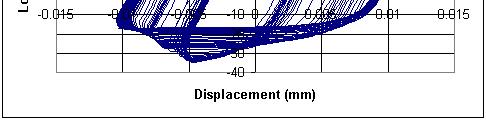
19

20
21
22 100 N f = 1468(W) (W) Strain Energy Density (MPa) (N f ) Number of Cycle-to-Failure

23 Free End Fixed End Symmetric
24 Laser (not shown) Beam steerer Thermal cycling Beam collumator Beamsplitter Digital camera Reference beam mirror
25 Time (s)

26 Long Axis - "Y" Short Axis "X"
27 Calculation (heating) Calculation (cooling) Test, X-disp Temperature (C)
28 SUMMARY? A systematic method for determining the thermal-fatigue life of the solder sealing ring in a photonic package has been provided.? A creep constitutive equation for the 48Sn-52In solder has been obtained.? Confidence of the present analysis procedures, material properties, boundary conditions and results has been demonstrated by comparing with experiment results obtained by the Twyman-Green interferometry method.? The fatigue material property (number of cycle-to-failure vs strain energy density per cycle) for the 48Sn-52In has been determined by the isothermal shearing fatigue tests.? By combining the finite element results (strain energy density per cycle) and the fatigue test results, the average thermal-fatigue life of the solder ring is determined to be 4,000 cycles. This is more than adequate for shipping/storing/handling the photonic package.
29 Thermal Analysis of Vertical-Cavity Surface-Emitting LED/VCSEL Assembly with Lead-Free Flip Chip Interconnects John H. Lau Agilent Technologies, San Jose, CA, USA S.W. Ricky Lee Hong Kong University of Science & Technology Clear Water Bay, Kowloon, Hong Kong PhoPack2002, Stanford University, CA, USA 7/14/2002
30 Objectives To determine the effects of interconnect materials and ambient temperature on the steady-state temperature distribution of a 2x2 area array parallel vertical-cavity surface-emitting LED/VCSEL assembly. The light sources are deposited on a GaAs chip, which is mounted on a Si-substrate with four flip chip solder joints. Two kinds of solders, namely, 63Sn-37Pb and 80Au-20Sn, are studied.
31 Outline of Presentation Introduction and Overview Description of Assembly Configuration Finite Element Modeling Thermal Analysis and Discussion Concluding Remarks
32 Introduction Fiber-Optic Communication Systems * Light Sources * Optical Fibers * Optical Receivers The electrical signal is converted into the optical signal through the light source. The optical signal is transmitted through the optical fiber. The optical signal is converted back into the electrical signal through the optical receiver.
33 Light Sources Most of the light sources are based on the electron-hole recombination in semiconductor materials. This recombination results in the release of energy (in the form of another photon), which can take place: SPONTANEOUSLY such as the light-emitting diodes (LEDs), which are used for very short distance such as chip-to-chip communications with plastic fibers. As a result of an EXTERNAL STIMULUS such as the semiconductor lasers, which are used for long distance telecommunications.
34 For both LEDs and semiconductor lasers, they can collect the light in the direction parallel to the p-n junction and are called the edge-emitting diodes and edge-emitting lasers, respectively. They can also collect the light in the direction perpendicular to the p-n junction and are called the surface-emitting diodes and vertical-cavity surface-emitting lasers (VCSELs), respectively. One of the advantages of surface-emitting light sources is that they can be used in parallel optics that offer low-cost interconnection with perhaps the best use of backplane space in a network system.
35 In principle, the wavelength in the infrared region has the advantage of integrating large 2-D emitter arrays with active (such as CMOS driver) components. This is because the semiconductor becomes transparent in this wavelength region and, therefore, the device can emit lights through the substrate. This feature yields to the possibility of applying the conventional flip chip technology to the LED/VCSEL assembly. One of the major advantages of solder-bumped flip chip technology is the self-alignment capability.

36 4x4 VCSEL Array with 16 Wire Bonds Courtesy of Honeywell

37 Configuration of VCSEL Assembly Light Emission GaAs Solder Joints Si Substrate (A quarter of the GaAs chip is removed to observe the solder joints)
38 Dimensions of VCSEL Assembly Si Substrate 1000 x 1000 x 200 µm GaAs 500 x 500 x 300 µm Solder Joint Array Pitch: 250 µm (2x2)

39 Finite Element Meshes GaAs AlGaAs Solder Joint Finite Element Mesh of a Quarter Whole VCSEL Assembly Local Finite Element Mesh of AlGaAs/Solder Joint/Cu Pad Cu Si
 80 µm AlGaAs 500 µm (Thickness: 200 µm) Solder Joints 80 µm (Thickness: 5 µm)")
40 Dimensions of Finite Element Model (Thickness: 300 µm) 250 µm Solder Bump Size: 100 µm Bump Height: 75 µm (Thickness: 5 µm) 80 µm AlGaAs 500 µm (Thickness: 200 µm) Solder Joints 80 µm (Thickness: 5 µm) Cu
41 Finite Element Thermal Analysis ANSYS V. 5.7 SOLID70 3-D 8-node Element Steady-State Thermal Conduction Heat Source: AlGaAs (1 mw) Ambient Temperature: 27 o C or 55 o C
42 Thermal Conductivity for Modeling
43 Temperature Contours (I) 63Sn-37Pb 80Au-20Sn Ambient Temperature = 27 o C

44 Temperature Contours (II) 63Sn-37Pb 80Au-20Sn Ambient Temperature = 55 o C
45 Consideration of Heat Convection Heat-Transfer Coefficients Ambient Temperature = 25 o C The back of the GaAs Chip = 1.017x10⁻⁵ W/ o C-mm 2 The side of the GaAs Chip = 2.662x10⁻⁵ W/ o C-mm 2 The top of the GaAs Chip = 2.662x10⁻⁵ W/ o C-mm 2 The back of the Si Chip = 2.163x10⁻⁵ W/ o C-mm 2 The side of the Si Chip = 2.662x10⁻⁵ W/ o C-mm 2 The top of the Si Chip = 1.017x10⁻⁵ W/ o C-mm 2 Ambient Temperature = 55 o C The back of the GaAs Chip = 0.982x10⁻⁵ W/ o C-mm 2 The side of the GaAs Chip = 2.596x10⁻⁵ W/ o C-mm 2 The top of the GaAs Chip = 2.596x10⁻⁵ W/ o C-mm 2 The back of the Si Chip = 2.142x10⁻⁵ W/ o C-mm 2 The side of the Si Chip = 2.596x10⁻⁵ W/ o C-mm 2 The top of the Si Chip = x10-5 W/ o C-mm 2
46 Concluding Remarks A new configuration of VCSEL assembly using solder-bumped flip chip interconnects is proposed A 3-D FE thermal analysis is performed to investigate the effect of solder materials and ambient temperature. 80Au-20Sn is a better choice than 63Sn-37Pb solder. The change of ambient temperature does not affect the pattern of temperature contours.
TABLE OF CONTENTS CHAPTER TITLE PAGE DECLARATION DEDICATION ACKNOWLEDGEMENT ABSTRACT ABSTRAK
 vii TABLE OF CONTENTS CHAPTER TITLE PAGE DECLARATION DEDICATION ACKNOWLEDGEMENT ABSTRACT ABSTRAK TABLE OF CONTENTS LIST OF TABLES LIST OF FIGURES LIST OF ABBREVIATIONS LIST OF SYMBOLS ii iii iv v vi vii
1 INTRODUCTION 2 SAMPLE PREPARATIONS
 Chikage NORITAKE This study seeks to analyze the reliability of three-dimensional (3D) chip stacked packages under cyclic thermal loading. The critical areas of 3D chip stacked packages are defined using
Stress in Flip-Chip Solder Bumps due to Package Warpage -- Matt Pharr
 Stress in Flip-Chip Bumps due to Package Warpage -- Matt Pharr Introduction As the size of microelectronic devices continues to decrease, interconnects in the devices are scaling down correspondingly.
Ratcheting deformation in thin film structures
 Ratcheting deformation in thin film structures Z. SUO Princeton University Work with MIN HUANG, Rui Huang, Jim Liang, Jean Prevost Princeton University Q. MA, H. Fujimoto, J. He Intel Corporation Interconnect
Impact of Uneven Solder Thickness on IGBT Substrate Reliability
 Impact of Uneven Solder Thickness on IGBT Substrate Reliability Hua Lu a, Chris Bailey a, Liam Mills b a Department of Mathematical Sciences, University of Greenwich 30 Park Row, London, SE10 9LS, UK b
Chapter 5: Ball Grid Array (BGA)
") Chapter 5: Ball Grid Array (BGA) 5.1 Development of the Models The following sequence of pictures explains schematically how the FE-model of the Ball Grid Array (BGA) was developed. Initially a single
Chapter 5: Ball Grid Array (BGA) 5.1 Development of the Models The following sequence of pictures explains schematically how the FE-model of the Ball Grid Array (BGA) was developed. Initially a single
Cyclic Bend Fatigue Reliability Investigation for Sn-Ag-Cu Solder Joints
 Cyclic Bend Fatigue Reliability Investigation for Sn-Ag-Cu Solder Joints F.X. Che* 1, H.L.J. Pang 2, W.H. Zhu 1 and Anthony Y. S. Sun 1 1 United Test & Assembly Center Ltd. (UTAC) Packaging Analysis &
Design of Power Electronics Reliability: A New, Interdisciplinary Approach. M.C. Shaw. September 5, 2002
 Design of Power Electronics Reliability: A New, Interdisciplinary Approach M.C. Shaw September 5, 2002 Physics Department California Lutheran University 60 W. Olsen Rd, #3750 Thousand Oaks, CA 91360 (805)
Critical Issues in Computational Modeling and Fatigue Life Analysisfor PBGA Solder Joints
 Critical Issues in Computational Modeling and Fatigue Life Analysis for PBGA Solder Joints Critical Issues in Computational Modeling and Fatigue Life Analysisfor PBGA Solder Joints Xiaowu Zhang and S-W.
314 IEEE TRANSACTIONS ON ADVANCED PACKAGING, VOL. 33, NO. 2, MAY Wei Tan, I. Charles Ume, Ying Hung, and C. F. Jeff Wu
 314 IEEE TRANSACTIONS ON ADVANCED PACKAGING, VOL. 33, NO. 2, MAY 2010 Effects of Warpage on Fatigue Reliability of Solder Bumps: Experimental and Analytical Studies Wei Tan, I. Charles Ume, Ying Hung,
Fatigue Properties of SIP Solder Joints
 Fatigue Properties of SIP Solder Joints 12th December 2007 Milos Dusek, Chris Hunt milos.dusek@npl.co.uk chris.hunt@npl.co.uk Presentation: Davide Di Maio Outline Isothermal Fatigue Life Cycling Profile
Reliability assessment for Cu/Low-k structure based on bump shear modeling and simulation method
 Reliability assessment for Cu/Low-k structure based on bump shear modeling and simulation method Abstract Bump shear is widely used to characterize interface strength of Cu/low-k structure. In this work,
The Reliability Analysis and Structure Design for the Fine Pitch Flip Chip BGA Packaging
 The Reliability Analysis and Structure Design for the Fine Pitch Flip Chip BGA Packaging Chih-Tang Peng 1, Chang-Ming Liu 1, Ji-Cheng Lin 1, Kuo-Ning Chiang E-Mail: Knchiang@pme.nthu.edu.tw Department
Constitutive and Damage Accumulation Modeling
 Workshop on Modeling and Data needs for Lead-Free Solders Sponsored by NEMI, NIST, NSF, and TMS February 15, 001 New Orleans, LA Constitutive and Damage Accumulation Modeling Leon M. Keer Northwestern
FYS4260/FYS9260: Microsystems and Electronics Packaging and Interconnect. Thermal Management
 FYS4260/FYS9260: Microsystems and Electronics Packaging and Interconnect Thermal Management Figure information preceeding page Free convection thermoelectric cooler (Peltier cooler) with heat sink surface
Semiconductor Disk Laser on Microchannel Cooler
 Semiconductor Disk Laser on Microchannel Cooler Eckart Gerster An optically pumped semiconductor disk laser with a double-band Bragg reflector mirror is presented. This mirror not only reflects the laser
High Power Diode Lasers
 Lecture 10/1 High Power Diode Lasers Low Power Lasers (below tenth of mw) - Laser as a telecom transmitter; - Laser as a spectroscopic sensor; - Laser as a medical diagnostic tool; - Laser as a write-read
FEM Analysis on Mechanical Stress of 2.5D Package Interposers
 Hisada et al.: FEM Analysis on Mechanical Stress of 2.5D Package Interposers (1/8) [Technical Paper] FEM Analysis on Mechanical Stress of 2.5D Package Interposers Takashi Hisada, Toyohiro Aoki, Junko Asai,
Strain Measurement. Prof. Yu Qiao. Department of Structural Engineering, UCSD. Strain Measurement
 Strain Measurement Prof. Yu Qiao Department of Structural Engineering, UCSD Strain Measurement The design of load-carrying components for machines and structures requires information about the distribution
Reliability analysis of different structure parameters of PCBA under drop impact
 Journal of Physics: Conference Series PAPER OPEN ACCESS Reliability analysis of different structure parameters of PCBA under drop impact To cite this article: P S Liu et al 2018 J. Phys.: Conf. Ser. 986
(b) Spontaneous emission. Absorption, spontaneous (random photon) emission and stimulated emission.
 Spontaneous emission. Absorption, spontaneous (random photon) emission and stimulated emission.") Lecture 10 Stimulated Emission Devices Lasers Stimulated emission and light amplification Einstein coefficients Optical fiber amplifiers Gas laser and He-Ne Laser The output spectrum of a gas laser Laser
Lecture 10 Stimulated Emission Devices Lasers Stimulated emission and light amplification Einstein coefficients Optical fiber amplifiers Gas laser and He-Ne Laser The output spectrum of a gas laser Laser
Introduction to Optoelectronic Device Simulation by Joachim Piprek
 NUSOD 5 Tutorial MA Introduction to Optoelectronic Device Simulation by Joachim Piprek Outline:. Introduction: VCSEL Example. Electron Energy Bands 3. Drift-Diffusion Model 4. Thermal Model 5. Gain/Absorption
Key words Lead-free solder, Microelectronic packaging, RF packaging, RoHS compliant, Solder joint reliability, Weibull failure distribution
 Solder Joint Reliability Assessment for a High Performance RF Ceramic Package Paul Charbonneau, Hans Ohman, Marc Fortin Sanmina Corporation 500 Palladium Dr. Ottawa, Ontario K2V 1C2 Canada Ph: 613-886-6000;
Metal Vapour Lasers Use vapoured metal as a gain medium Developed by W. Silfvast (1966) Two types: Ionized Metal vapour (He-Cd) Neutral Metal vapour
 Two types: Ionized Metal vapour (He-Cd) Neutral Metal vapour") Metal Vapour Lasers Use vapoured metal as a gain medium Developed by W. Silfvast (1966) Two types: Ionized Metal vapour (He-Cd) Neutral Metal vapour (Cu) All operate by vaporizing metal in container Helium
Metal Vapour Lasers Use vapoured metal as a gain medium Developed by W. Silfvast (1966) Two types: Ionized Metal vapour (He-Cd) Neutral Metal vapour (Cu) All operate by vaporizing metal in container Helium
Reliability Analysis of Moog Ultrasonic Air Bubble Detectors
 Reliability Analysis of Moog Ultrasonic Air Bubble Detectors Air-in-line sensors are vital to the performance of many of today s medical device applications. The reliability of these sensors should be
The Increasing Importance of the Thermal Management for Modern Electronic Packages B. Psota 1, I. Szendiuch 1
 Ročník 2012 Číslo VI The Increasing Importance of the Thermal Management for Modern Electronic Packages B. Psota 1, I. Szendiuch 1 1 Department of Microelectronics, Faculty of Electrical Engineering and
Prediction of Encapsulant Performance Toward Fatigue Properties of Flip Chip Ball Grid Array (FC-BGA) using Accelerated Thermal Cycling (ATC)
 using Accelerated Thermal Cycling (ATC)") Prediction of Encapsulant Performance Toward Fatigue Properties of Flip Chip Ball Grid Array (FC-BGA) using Accelerated Thermal Cycling (ATC) ZAINUDIN KORNAIN 1, AZMAN JALAR 2,3, SHAHRUM ABDULLAH 3, NOWSHAD
Prediction of Encapsulant Performance Toward Fatigue Properties of Flip Chip Ball Grid Array (FC-BGA) using Accelerated Thermal Cycling (ATC) ZAINUDIN KORNAIN 1, AZMAN JALAR 2,3, SHAHRUM ABDULLAH 3, NOWSHAD
Simulation of the Influence of Manufacturing Quality on Thermomechanical Stress of Microvias
 As originally published in the IPC APEX EXPO Conference Proceedings. Simulation of the Influence of Manufacturing Quality on Thermomechanical Stress of Microvias Yan Ning, Michael H. Azarian, and Michael
Next-Generation Packaging Technology for Space FPGAs
 Power Matters. Next-Generation Packaging Technology for Space FPGAs Microsemi Space Forum Russia November 2013 Raymond Kuang Director of Packaging Engineering, SoC Products Group Agenda CCGA (ceramic column
Thermo-Mechanical Analysis of a Multi-Layer MEMS Membrane
 Thermo-Mechanical Analysis of a Multi-Layer MEMS Membrane Heiko Fettig, PhD James Wylde, PhD Nortel Networks - Optical Components Ottawa ON K2H 8E9 Canada Abstract This paper examines the modelling of
Deformation of solder joint under current stressing and numerical simulation II
 International Journal of Solids and Structures 41 (2004) 4959 4973 www.elsevier.com/locate/ijsolstr Deformation of solder joint under current stressing and numerical simulation II Hua Ye *, Cemal Basaran,
Blue-green Emitting Semiconductor Disk Lasers with Intra-Cavity Frequency Doubling
 Blue-green Emitting Semiconductor Disk Lasers with Intra-Cavity Frequency Doubling Eckart Schiehlen and Michael Riedl Diode-pumped semiconductor disk lasers, also referred to as VECSEL (Vertical External
AOS Semiconductor Product Reliability Report
 AOS Semiconductor Product Reliability Report AO64/AO64L, rev C Plastic Encapsulated Device ALPHA & OMEGA Semiconductor, Inc 49 Mercury Drive Sunnyvale, CA 948 U.S. Tel: (48) 83-9742 www.aosmd.com Mar 8,
[5] Stress and Strain
![[5] Stress and Strain](/thumbs/95/123344550.jpg "[5] Stress and Strain") [5] Stress and Strain Page 1 of 34 [5] Stress and Strain [5.1] Internal Stress of Solids [5.2] Design of Simple Connections (will not be covered in class) [5.3] Deformation and Strain [5.4] Hooke s Law
[5] Stress and Strain Page 1 of 34 [5] Stress and Strain [5.1] Internal Stress of Solids [5.2] Design of Simple Connections (will not be covered in class) [5.3] Deformation and Strain [5.4] Hooke s Law
Assessment of Soft Errors due to Alpha Emissions from Presolder on Flip Chip Devices Rick Wong, Shi-Jie Wen, Peng Su, Li Li 10/30/09
 Assessment of Soft Errors due to Alpha Emissions from Presolder on Flip Chip Devices Rick Wong, Shi-Jie Wen, Peng Su, Li Li 10/30/09 1 Introduction Cause of Soft errors a. Ion creates electron hole pairs
Laser Basics. What happens when light (or photon) interact with a matter? Assume photon energy is compatible with energy transition levels.
 interact with a matter? Assume photon energy is compatible with energy transition levels.") What happens when light (or photon) interact with a matter? Assume photon energy is compatible with energy transition levels. Electron energy levels in an hydrogen atom n=5 n=4 - + n=3 n=2 13.6 = [ev]
What happens when light (or photon) interact with a matter? Assume photon energy is compatible with energy transition levels. Electron energy levels in an hydrogen atom n=5 n=4 - + n=3 n=2 13.6 = [ev]
Tools for Thermal Analysis: Thermal Test Chips Thomas Tarter Package Science Services LLC
 Tools for Thermal Analysis: Thermal Test Chips Thomas Tarter Package Science Services LLC ttarter@pkgscience.com INTRODUCTION Irrespective of if a device gets smaller, larger, hotter or cooler, some method
Outline. 4 Mechanical Sensors Introduction General Mechanical properties Piezoresistivity Piezoresistive Sensors Capacitive sensors Applications
 Sensor devices Outline 4 Mechanical Sensors Introduction General Mechanical properties Piezoresistivity Piezoresistive Sensors Capacitive sensors Applications Introduction Two Major classes of mechanical
ECE 695 Numerical Simulations Lecture 35: Solar Hybrid Energy Conversion Systems. Prof. Peter Bermel April 12, 2017
 ECE 695 Numerical Simulations Lecture 35: Solar Hybrid Energy Conversion Systems Prof. Peter Bermel April 12, 2017 Ideal Selective Solar Absorber Efficiency Limits Ideal cut-off wavelength for a selective
Thermal Sensors and Actuators
 Thermal Sensors and Actuators Part I Fundamentals of heat transfer Heat transfer occurs where there is a temperature gradient until an equilibrium is reached. Four major mechanism Thermal conduction Natural
New Functions. Test mode and Specimen failure. Power cycle test system with thermal analysis capability using structure function.
 using structure function. (1) Page 1/5 Test mode and failure There are two modes in a power cycle test: Tj Power cycle that changes the junction temperature (Tj Temperature) inside of the power semiconductor
Drop Impact Reliability Test and Failure Analysis for Large Size High Density FOWLP Package on Package
 2017 IEEE 67th Electronic Components and Technology Conference Drop Impact Reliability Test and Failure Analysis for Large Size High Density FOWLP Package on Package Zhaohui Chen, Faxing Che, Mian Zhi
AOS Semiconductor Product Reliability Report
 AOS Semiconductor Product Reliability Report AO4466/AO4466L, rev B Plastic Encapsulated Device ALPHA & OMEGA Semiconductor, Inc 49 Mercury Drive Sunnyvale, CA 948 U.S. Tel: (48) 83-9742 www.aosmd.com Jun
Mechanical Analysis Challenges in Micro-Electronic Packaging
 Mechanical Analysis Challenges in Micro-Electronic Packaging Luke J. Garner, and Frank Z. Liang Intel Corporation Electrical and thermal performance enhancing features in modern integrated circuits have
Stimulated Emission Devices: LASERS
 Stimulated Emission Devices: LASERS 1. Stimulated Emission and Photon Amplification E 2 E 2 E 2 hυ hυ hυ In hυ Out hυ E 1 E 1 E 1 (a) Absorption (b) Spontaneous emission (c) Stimulated emission The Principle
Thermo-structural Model of Stacked Field-programmable Gate Arrays (FPGAs) with Through-silicon Vias (TSVs)
 with Through-silicon Vias (TSVs)") Manuscript for Review Thermo-structural Model of Stacked Field-programmable Gate Arrays (FPGAs) with Through-silicon Vias (TSVs) Journal: Electronics Letters Manuscript ID: draft Manuscript Type: Letter
Manuscript for Review Thermo-structural Model of Stacked Field-programmable Gate Arrays (FPGAs) with Through-silicon Vias (TSVs) Journal: Electronics Letters Manuscript ID: draft Manuscript Type: Letter
Temperature Cycling Analysis of Lead-Free Solder Joints in Electronic Packaging
 Temperature Cycling Analysis of Lead-Free Solder Joints in Electronic Packaging Shan Li a,*, Zhenyu Huang a and Jianfeng Wang a,shaowu Gao b a Intel (Shanghai) Technology Development Ltd., Shanghai, China
Reliability Evaluation Method for Electronic Device BGA Package Considering the Interaction Between Design Factors
 Reliability Evaluation Method for Electronic Device BGA Package Considering the Interaction Between Design Factors Satoshi KONDO *, Qiang YU *, Tadahiro SHIBUTANI *, Masaki SHIRATORI * *Department of Mechanical
TCAD Modeling of Stress Impact on Performance and Reliability
 TCAD Modeling of Stress Impact on Performance and Reliability Xiaopeng Xu TCAD R&D, Synopsys March 16, 2010 SEMATECH Workshop on Stress Management for 3D ICs using Through Silicon Vias 1 Outline Introduction
Signal regeneration - optical amplifiers
 Signal regeneration - optical amplifiers In any atom or solid, the state of the electrons can change by: 1) Stimulated absorption - in the presence of a light wave, a photon is absorbed, the electron is
A Note on Suhir s Solution of Thermal Stresses for a Die-Substrate Assembly
 M. Y. Tsai e-mail: mytsai@mail.cgu.edu.tw C. H. Hsu C. N. Han Department of Mechanical Engineering, Chang Gung University, Kwei-Shan, Tao-Yuan, Taiwan 333, ROC A Note on Suhir s Solution of Thermal Stresses
ADVANCED BOARD LEVEL MODELING FOR WAFER LEVEL PACKAGES
 As originally published in the SMTA Proceedings ADVANCED BOARD LEVEL MODELING FOR WAFER LEVEL PACKAGES Tiao Zhou, Ph.D. Southern Methodist University Dallas, TX, USA tiaoz@smu.edu Zhenxue Han, Ph.D. University
What are Carbon Nanotubes? What are they good for? Why are we interested in them?
 Growth and Properties of Multiwalled Carbon Nanotubes What are Carbon Nanotubes? What are they good for? Why are we interested in them? - Interconnects of the future? - our vision Where do we stand - our
Metal Vapour Lasers Use vapourized metal as a gain medium Developed by W. Silfvast (1966) Put metal in a cavity with a heater Vapourize metal, then
 Put metal in a cavity with a heater Vapourize metal, then") Metal Vapour Lasers Use vapourized metal as a gain medium Developed by W. Silfvast (1966) Put metal in a cavity with a heater Vapourize metal, then pump metal vapour with current Walter at TRG (1966) then
Metal Vapour Lasers Use vapourized metal as a gain medium Developed by W. Silfvast (1966) Put metal in a cavity with a heater Vapourize metal, then pump metal vapour with current Walter at TRG (1966) then
Electron Energy, E E = 0. Free electron. 3s Band 2p Band Overlapping energy bands. 3p 3s 2p 2s. 2s Band. Electrons. 1s ATOM SOLID.
 Electron Energy, E Free electron Vacuum level 3p 3s 2p 2s 2s Band 3s Band 2p Band Overlapping energy bands Electrons E = 0 1s ATOM 1s SOLID In a metal the various energy bands overlap to give a single
A Guide to Board Layout for Best Thermal Resistance for Exposed Packages
 A Guide to Board Layout for Best Thermal Resistance for Exposed Packages Table of Contents 1.0 Abstract... 2 2.0 Introduction... 2 3.0 DOE of PCB (Printed Circuit Board) Design... 2 4.0 Test Methodology...
Thermal Characterization of Packaged RFIC, Modeled vs. Measured Junction to Ambient Thermal Resistance
 Thermal Characterization of Packaged RFIC, Modeled vs. Measured Junction to Ambient Thermal Resistance Steven Brinser IBM Microelectronics Abstract Thermal characterization of a semiconductor device is
ELEC 4700 Assignment #2
 ELEC 4700 Assignment #2 Question 1 (Kasop 4.2) Molecular Orbitals and Atomic Orbitals Consider a linear chain of four identical atoms representing a hypothetical molecule. Suppose that each atomic wavefunction
Modal and Harmonic Response Analysis of PBGA and S-N Curve Creation of Solder Joints
 Sensors & Transducers 2013 by IFSA http://www.sensorsportal.com Modal and Harmonic Response Analysis of PBGA and S-N Curve Creation of Solder Joints 1 Yu Guo, 1 Kailin Pan, 1, 2 Xin Wang, 1, 2 Tao Lu and
Budapest, Hungary, September 2007 The Characteristics of Electromigration And Thermomigration in Flip Chip Solder Joints
 The Characteristics of Electromigration And Thermomigration in Flip Chip Solder Joints Dan Yang and Y. C. Chan* Department of Electronic Engineering, City University of Hong Kong, 83 Tat Chee Avenue, Kowloon,
Mar Yunsu Sung. Yunsu Sung. Special Topics in Optical Engineering II(15/1)
") Mar 12 2015 Contents Two-port model Rate equation and damping Small signal response Conclusion Two Port Model I:Current V:Voltage P: Optical Power ν: Optical frequency shift Model summarize parasitic effects
Mar 12 2015 Contents Two-port model Rate equation and damping Small signal response Conclusion Two Port Model I:Current V:Voltage P: Optical Power ν: Optical frequency shift Model summarize parasitic effects
Available online at ScienceDirect. XVII International Colloquium on Mechanical Fatigue of Metals (ICMFM17)
") Available online at www.sciencedirect.com ScienceDirect Procedia Engineering 74 ( 2014 ) 165 169 XVII International Colloquium on Mechanical Fatigue of Metals (ICMFM17) Fatigue of Solder Interconnects
Available online at www.sciencedirect.com ScienceDirect Procedia Engineering 74 ( 2014 ) 165 169 XVII International Colloquium on Mechanical Fatigue of Metals (ICMFM17) Fatigue of Solder Interconnects
IS2805 DESCRIPTION FEATURES
 DESCRIPTION The is an optically coupled isolator consists of two infrared emitting diodes in reverse parallel connection and optically coupled to an NPN silicon photo transistor. This device belongs to
Chapter 7. Solar Cell
 Chapter 7 Solar Cell 7.0 Introduction Solar cells are useful for both space and terrestrial application. Solar cells furnish the long duration power supply for satellites. It converts sunlight directly
3.1 Absorption and Transparency
 3.1 Absorption and Transparency 3.1.1 Optical Devices (definitions) 3.1.2 Photon and Semiconductor Interactions 3.1.3 Photon Intensity 3.1.4 Absorption 3.1 Absorption and Transparency Objective 1: Recall
Thermal Resistance Measurement
 Optotherm, Inc. 2591 Wexford-Bayne Rd Suite 304 Sewickley, PA 15143 USA phone +1 (724) 940-7600 fax +1 (724) 940-7611 www.optotherm.com Optotherm Sentris/Micro Application Note Thermal Resistance Measurement
Thermal-Mechanical Analysis of a Different Leadframe Thickness of Semiconductor Package under the Reflow Process
 American Journal of Applied Sciences 6 (4): 616-625, 2009 ISSN 1546-9239 2009 Science Publications Thermal-Mechanical Analysis of a Different Leadframe Thickness of Semiconductor Package under the Reflow
Shorter Field Life in Power Cycling for Organic Packages
 Shorter Field Life in Power Cycling for Organic Packages S. B. Park e-mail: sbpark@binghamton.edu Izhar Z. Ahmed Department of Mechanical Engineering, State University of New York at Binghamton, Binghamton,
OPTICAL PROPERTIES OF THE DIRC FUSED SILICA CHERENKOV RADIATOR
 OPTICAL PROPERTIES OF THE DIRC FUSED SILICA CHERENKOV RADIATOR J. Cohen-Tanugi, M. Convery, B. Ratcliff, X. Sarazin, J. Schwiening, and J. Va'vra * Stanford Linear Accelerator Center, Stanford University,
Mechanical Simulations for Chip Package Interaction: Failure Mechanisms, Material Characterization, and Failure Data
 Mechanical Simulations for Chip Package Interaction: Failure Mechanisms, Material Characterization, and Failure Data Ahmer Syed Amkor Technology Enabling a Microelectronic World Outline Effect of Chip
Chapter 7 Mechanical Characterization of the Electronic Packages
 Chapter 7 Mechanical Characterization of the Electronic Packages 1 3 Thermal Mismatch Si (CTE=~3 ppm/c) Underfill (CTE=7 ppm/c) EU solder (CTE=5 ppm/c) Substrate (CTE=15~0 ppm/c) Thermal mismatch in electronic
[ ] Sensors for Temperature Measurement, and Their Application 2L R 1 1 T 1 T 2
![[ ] Sensors for Temperature Measurement, and Their Application 2L R 1 1 T 1 T 2](/thumbs/89/97951344.jpg "[ ] Sensors for Temperature Measurement, and Their Application 2L R 1 1 T 1 T 2") Sensors for Temperature Measurement, and Their Application In today s market, it is very rare to see electronic equipment that has not undergone extensive thermal evaluation, either by measurement or simulation.
Sensors for Temperature Measurement, and Their Application In today s market, it is very rare to see electronic equipment that has not undergone extensive thermal evaluation, either by measurement or simulation.
Assessment of Current Density Singularity in Electromigration of Solder Bumps
 Assessment of Current Density Singularity in Electromigration of Solder Bumps Pridhvi Dandu and Xuejun Fan Department of Mechanical Engineering Lamar University PO Box 10028, Beaumont, TX 77710, USA Tel:
THE demand for plastic packages has increased due to
 294 IEEE TRANSACTIONS ON COMPONENTS AND PACKAGING TECHNOLOGIES, VOL. 30, NO. 2, JUNE 2007 Predictive Model for Optimized Design Parameters in Flip-Chip Packages and Assemblies Seungbae Park, H. C. Lee,
An Engelmaier Model for Leadless Ceramic Chip Devices with Pb-free Solder
 An Engelmaier Model for Leadless Ceramic Chip Devices with Pb-free Solder Nathan Blattau and Craig Hillman DfR Solutions 5110 Roanoke Place, Suite 101 College Park, MD 20740 nblattau@dfrsolutions.com ABSTRACT
Introduction to semiconductor nanostructures. Peter Kratzer Modern Concepts in Theoretical Physics: Part II Lecture Notes
 Introduction to semiconductor nanostructures Peter Kratzer Modern Concepts in Theoretical Physics: Part II Lecture Notes What is a semiconductor? The Fermi level (chemical potential of the electrons) falls
Published by: PIONEER RESEARCH & DEVELOPMENT GROUP(
 MEMS based Piezo resistive Pressure Sensor Swathi Krishnamurthy 1, K.V Meena 2, E & C Engg. Dept., The Oxford College of Engineering, Karnataka. Bangalore 560009 Abstract The paper describes the performance
Fabrication Technology, Part I
 EEL5225: Principles of MEMS Transducers (Fall 2004) Fabrication Technology, Part I Agenda: Microfabrication Overview Basic semiconductor devices Materials Key processes Oxidation Thin-film Deposition Reading:
The Stress Field Characteristics in the Surface Mount Solder Joints under Temperature Cycling: Temperature Effect and Its Evaluation
 SUPPLEMENT TO THE WELDING JOURNL, JUNE 2002 Sponsored by the merican Welding Society and the Welding Research Council The Stress Field Characteristics in the Surface Mount Solder Joints under Temperature
F. G. Marín, D Whalley, H Kristiansen and Z. L. Zhang, Mechanical Performance of Polymer Cored BGA Interconnects, Proceedings of the 10th Electronics
 F. G. Marín, D Whalley, H Kristiansen and Z. L. Zhang, Mechanical Performance of Polymer Cored BGA Interconnects, Proceedings of the 1th Electronics Packaging Technology Conference, 28. Mechanical Performance
How to measure packaging-induced strain in high-brightness diode lasers?
 How to measure packaging-induced strain in high-brightness diode lasers? Jens W. Tomm Max-Born-Institut für Nichtlineare Optik und Kurzzeitspektroskopie Berlin Max-Born-Str. 2 A, D-12489 Berlin, Germany
Introduction to Microeletromechanical Systems (MEMS) Lecture 9 Topics. MEMS Overview
 Lecture 9 Topics. MEMS Overview") Introduction to Microeletromechanical Systems (MEMS) Lecture 9 Topics MicroOptoElectroMechanical Systems (MOEMS) Grating Light Valves Corner Cube Reflector (CCR) MEMS Light Modulator Optical Switch Micromirrors
Introduction to Microeletromechanical Systems (MEMS) Lecture 9 Topics MicroOptoElectroMechanical Systems (MOEMS) Grating Light Valves Corner Cube Reflector (CCR) MEMS Light Modulator Optical Switch Micromirrors
SCB10H Series Pressure Elements PRODUCT FAMILY SPEFICIFATION. Doc. No B
 PRODUCT FAMILY SPEFICIFATION SCB10H Series Pressure Elements SCB10H Series Pressure Elements Doc. No. 82 1250 00 B Table of Contents 1 General Description... 3 1.1 Introduction... 3 1.2 General Description...
Woon-Seong Kwon Myung-Jin Yim Kyung-Wook Paik
 Woon-Seong Kwon e-mail: wskwon@kaist.ac.kr Myung-Jin Yim Kyung-Wook Paik Department of Materials Science and Engineering Korea Advanced Institute of Science and Technology Daejon 305-701, Korea Suk-Jin
Lecture 18. New gas detectors Solid state trackers
 Lecture 18 New gas detectors Solid state trackers Time projection Chamber Full 3-D track reconstruction x-y from wires and segmented cathode of MWPC z from drift time de/dx information (extra) Drift over
Mechanical characterization of single crystal BaTiO 3 film and insitu. XRD observation of microstructure change due to
 76 Chapter 4 Mechanical characterization of single crystal BaTiO 3 film and insitu XRD observation of microstructure change due to mechanical loading 4.1 Introduction Ferroelectric materials have many
Effects of Chrome Pattern Characteristics on Image Placement due to the Thermomechanical Distortion of Optical Reticles During Exposure
 Effects of Chrome Pattern Characteristics on Image Placement due to the Thermomechanical Distortion of Optical Reticles During Exposure A. Abdo, ab L. Capodieci, a I. Lalovic, a and R. Engelstad b a Advanced
OPTI510R: Photonics. Khanh Kieu College of Optical Sciences, University of Arizona Meinel building R.626
 OPTI510R: Photonics Khanh Kieu College of Optical Sciences, University of Arizona kkieu@optics.arizona.edu Meinel building R.626 Announcements HW#3 is assigned due Feb. 20 st Mid-term exam Feb 27, 2PM
Sensitivity analysis on the fatigue life of solid state drive solder joints by the finite element method and Monte Carlo simulation
 https://doi.org/10.1007/s00542-018-3819-0 (0456789().,-volV)(0456789().,-volV) TECHNICAL PAPER Sensitivity analysis on the fatigue life of solid state drive solder joints by the finite element method and
Technical Notes. Introduction. PCB (printed circuit board) Design. Issue 1 January 2010
 Design. Issue 1 January 2010") Technical Notes Introduction Thermal Management for LEDs Poor thermal management can lead to early LED product failure. This Technical Note discusses thermal management techniques and good system design.
Technical Notes Introduction Thermal Management for LEDs Poor thermal management can lead to early LED product failure. This Technical Note discusses thermal management techniques and good system design.
Bending Load & Calibration Module
 Bending Load & Calibration Module Objectives After completing this module, students shall be able to: 1) Conduct laboratory work to validate beam bending stress equations. 2) Develop an understanding of
CLCC Solder Joint Life Prediction under Complex Temperature Cycling Loading
 CLCC Solder Joint Life Prediction under Complex Temperature Cycling Loading, Michael Osterman, and Michael Pecht Center for Advanced Life Cycle Engineering (CALCE) University of Maryland College Park,
What do we study and do?
 What do we study and do? Light comes from electrons transitioning from higher energy to lower energy levels. Wave-particle nature of light Wave nature: refraction, diffraction, interference (labs) Particle
EE C247B / ME C218 INTRODUCTION TO MEMS DESIGN SPRING 2014 C. Nguyen PROBLEM SET #4
 Issued: Wednesday, Mar. 5, 2014 PROBLEM SET #4 Due (at 9 a.m.): Tuesday Mar. 18, 2014, in the EE C247B HW box near 125 Cory. 1. Suppose you would like to fabricate the suspended cross beam structure below
TRENDS IN LEVENSDUURTESTEN VOOR MICRO-ELEKTRONICA PLOT CONFERENTIE
 TRENDS IN LEVENSDUURTESTEN VOOR MICRO-ELEKTRONICA PLOT CONFERENTIE JEROEN JALINK 8 JUNI 2016 MICROELECTRONICS RELIABILITY 54 (2014) 1988 1994 Contents Introduction NXP Package form factor Failure mechanism
Fatigue Life Evaluation of Lead-free Solder under Thermal and Mechanical Loads
 Fatigue Life Evaluation of Lead-free Solder under Thermal and Mechanical Loads Ilho Kim and Soon-Bok Lee* Department of Mechanical Engineering, Korea Advanced Institute of Science and Technology 373-,
Especial Bump Bonding Technique for Silicon Pixel Detectors
 Especial Bump Bonding Technique for Silicon Pixel Detectors E. Cabruja, M. Bigas, M. Ullán, G. Pellegrini, M. Lozano Centre Nacional de Microelectrònica Spain Outline Motivation Summary of bump bonding
Multi-chip Integration on a PLC Platform for 16X16 Port Optical Switch Using Passive Alignment Technique
 Multi-chip Integration on a PLC Platform for 16X16 Port Optical Switch Using Passive Alignment Technique Jung Woon Lim, Hwe Jong Kim, Seon Hoon Kim and Byung Sup Rho Korea Photonics Technology Institute
Two Tier projects for students in ME 160 class
 ME 160 Introduction to Finite Element Method Spring 2016 Topics for Term Projects by Teams of 2 Students Instructor: Tai Ran Hsu, Professor, Dept. of Mechanical engineering, San Jose State University,
Study of Steady and Transient Thermal Behavior of High Power Semiconductor Lasers
 Study of Steady and Transient Thermal Behavior of High Power Semiconductor Lasers Zhenbang Yuan a, Jingwei Wang b, Di Wu c, Xu Chen a, Xingsheng Liu b,c a School of Chemical Engineering & Technology of